N A N O E X P R E S S
Open Access
Demonstration of Logic Operations in
High-Performance RRAM Crossbar Array
Fabricated by Atomic Layer Deposition
Technique
Runze Han, Peng Huang, Yudi Zhao, Zhe Chen, Lifeng Liu, Xiaoyan Liu and Jinfeng Kang
*Abstract
In this paper, resistive random access memory (RRAM)-based crossbar arrays with the cell structure of Pt/[AlOy/HfOx]m/ TiN were fabricated by using atomic layer deposition (ALD) technique. The RRAM devices in the arrays show excellent performances such as good uniformity and high reliability. Based on the fabricated RRAM array, a complete set of basic logic operations including NOR and XNOR were successfully demonstrated.
Keywords:RRAM, Crossbar, Atomic layer deposition (ALD), Logic operation
Background
Resistive random access memory (RRAM) is regarded as one of the most promising candidates for next gener-ation non-volatile memory due to its advantages such as low cost, fast write/read speed, low-energy consumption, and easy 3D integration [1–4]. In addition to the most common application as memory, RRAM can also be ap-plied to artificial neural network [5], mixed signal com-puting [6], and logic operation [7–10]. To perform logic operations, the combinations of a few devices in a cross-bar array are needed [10]. This characteristic makes it suitable for highly compact crossbar arrays with a 4F2 cell area (F is the minimum feature size) [11]. During logic computing process, each cell in a RRAM crossbar array can be used as input, output, assistance, and ory at different stages [8, 10]. This computing in mem-ory ability of the RRAM crossbar array will greatly reduce the time and energy consumption in the data shuttling process between the processing unit and mem-ory [12], thus making RRAM crossbar arrays appealing for developing beyond traditional von Neumann com-puting architectures [8–10, 13, 14].
However, implementation of logic operations in the RRAM crossbar array also brings challenges for RRAM
devices such as reducing device variability, improving de-vice yield, enlarging switching endurance etc. [10, 15, 16]. Former works demonstrated that HfOx thin films with
embedded Al layers will lead to better device uniformity [17, 18]. In this work, we use ALD technique to deposit a uniform and ultrathin AlOy/HfOx stacked resistive layer
([AlOy/HfOx]m). The fabricated RRAM crossbar array
with structure of Pt/[AlOy/HfOx]m/TiN shows excellent
device performances such as large resistance window (>80), uniform switching voltage, high switching endur-ance (>107cycles), high-disturbance immunity (>109 cy-cles), and good retention (>105s at 150 °C). Based on the fabricated RRAM crossbar array, a complete set of basic logic operations including NOR and XNOR were success-fully demonstrated.
Methods
The structure of a single device in the fabricated RRAM crossbar array is shown in Fig. 1a. The sputtered Ti/Pt layers were used for adhesion and bottom electrode, respectively. AlOy and HfOx were deposited layer by layer using ALD (Picosun R-200, Masala, Finland) tech-nique at 300 °C. H2O and trimethylaluminum (TMA)/ tetrakis[ethylmethylamino]hafnium (TEMAH) were used as precursors, respectively. This process was repeated for 10 times, so the final composition of the resistive layer is [AlOy/HfOx]m(m= 10). The total thickness of AlOy and
* Correspondence:[email protected]
Institute of Microelectronics, Peking University, Beijing 100871, China
© The Author(s). 2017Open AccessThis article is distributed under the terms of the Creative Commons Attribution 4.0 International License (http://creativecommons.org/licenses/by/4.0/), which permits unrestricted use, distribution, and reproduction in any medium, provided you give appropriate credit to the original author(s) and the source, provide a link to the Creative Commons license, and indicate if changes were made.
Hanet al. Nanoscale Research Letters (2017) 12:37
HfOx layers are 3 and 2 nm, respectively. The
PECVD-deposited SiO2layer was utilized to isolate resistive layers of different devices. Forty-nanometer TiN top electrode was then sputtered, followed by 100-nm Al contact layer sputtered on TiN. Except of the ALD process for the re-sistive layer deposition, the rest of the sample fabrication was reported in detail in Ref. [19]. Finally, the fabricated 16 × 2 RRAM crossbar array was packaged by using chip on board bonding method. The packaged crossbar array is shown in Fig. 1b. Note in Fig. 1b, the left and right side represent two crossbar arrays. The contact pads on the left/right side are word lines, while the contact pads on the top side are bit lines.
Electrical measurements were performed by Keysight B1500A semiconductor parameter analyzer (Keysight Technologies, Inc., Santa Clara, CA, USA).and Keysight 81160A pulse pattern and function arbitrary noise generator.
Results and Discussion
Device Performances Uniformity
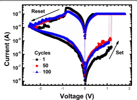
Uniformity is a major concern for logic computing. A tight set voltage distribution will make it easier to choose proper amplitudes of reference voltage applied on the in-put cell and the supply voltage applied on the outin-put cell. Therefore, the misconduct of the output cell will be avoided. The variation exists in the low resistance and high resistance of the RRAM will reduce the resistance window. With a reduced resistance window, the accuracy of the logic operating will be reduced too. So, a uniform resistance distribution is also important for logic oper-ation. The typical DC I–V curves of the RRAM device are shown in Fig. 2. A positive voltage above set voltage (VSET) was applied to make the resistance state of RRAM transit from high-resistance state (HRS) to low-resistance state (LRS). During set operation, the current flow
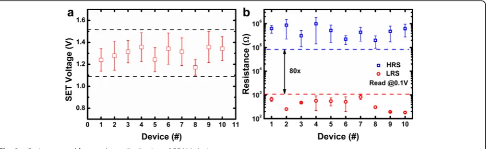
through the device is limited to 1 mA to control the fila-ment shape and prevent permanent breakdown. After set transition, a negative voltage lower than reset voltage (VRESET) was applied on the device to switch it from LRS to HRS. The good consistency among I–V curves in cycles 1, 50, and 100 reveals excellent cycle-to-cycle switching uniformity of RRAM devices. To investigate the device-to-device variability of fabricated devices, set voltage and resistance distribution of 10 randomly chosen RRAM de-vices in a crossbar array was tested. To extract the set voltage, a −1.9 V,100 ns voltage pulse was firstly applied on the RRAM device to switch it to a HRS, then a set pulse train with 100-ns width was applied. Set pulse amp-litude increases from 0.8 V with a step voltage of 0.05 V; after each step, a read voltage was applied to read its re-sistance state. When the rere-sistance is lower than a set value (2kΩ), the set pulse amplitude increase stops and the current voltage pulse amplitude was marked as the set voltage. The test result is shown in Fig. 3a. A uniform set voltage distribution range from 1.1 to 1.5 V was measured. Fig. 1aThe fabricated RRAM device structure.bThe packaged RRAM crossbar array
[image:2.595.56.540.87.262.2] [image:2.595.307.537.545.713.2]According to the measured set voltage distribution, the re-sistance distribution was tested under 1.6 V,100 ns set pulses and−1.9 V,100 ns reset pulses. The test result sug-gests that despite cycle-to-cycle and device-to-device vari-ability, RRAM devices still hold a resistance window larger than 80, as is illustrated in Fig. 3b. The excellent uniformity exhibited in these devices is mainly due to the introduction of Al atoms into HfOx layers. Because the
formation and rupture of the conduction filament consists of oxygen vacancies (VO) has been widely recognized as the switching mechanism, while with the diffusion of Al into HfOx layers, the formation energy of oxygen vacan-cies will be reduced. Therefore, the device uniformity will be improved with more controllable conduction filaments formed steadily along Al atoms [17].
Reliability
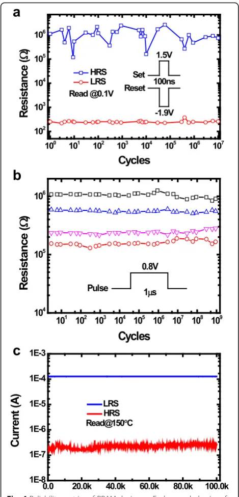
Reliability is another major consideration to build robust computing systems based on RRAM. RRAM devices have to be switched for many times in the computing process, so a good endurance behavior is important. To test the endurance behavior, a 1.5 V,100 ns set voltage pulse was applied on the RRAM device to make it tran-sit from HRS to LRS, then a −1.9 V,100 ns reset pulse was applied to change the resistance state to HRS, this process was repeated for many times. The test result suggests fabricated RRAM devices could switch nor-mally after 107consecutive switching, which is shown in Fig. 4a. Because the doping of Al atoms in HfOx layers
will lead to lower formation energy and more control-lable filament shape, then the conduction filament will become more recoverable, so the endurance will be en-hanced [20]. During logic computing, half supply voltage is applied on the input cell, thus will cause disturbance [10, 21]. Good disturbance immunity ensures the logic state of the input cell will not be changed with applied voltage disturbance. The disturbance behavior is tested under repeated 0.8 V, 1μs disturbance pulses. Figure 4b shows excellent disturbance immunity of RRAM devices
for over 109 disturb cycles with different initial resist-ance ranges from 0.1 to 1MΩ. To ensure the logic state of the computing cell being correctly sensed, a good re-tention behavior is needed. Excellent rere-tention behavior for LRS and HRS was measured for up to 105s at the temperature 150 °C, which is shown in Fig. 4c.
Demonstration of Logic Operations
The set containing NOR suffices as a complete logic set. Any other logic operation can be realized through com-binations of NOR logic. Circuit realization of NOR logic operation is shown in Fig. 5a. Three RRAM devices were used with two input cells marked as A and B and one output cell marked as Y. The common bit line is serially connected to GND through a load resistance RC. To guarantee the logic operation works correctly, the volt-age should fall mainly on the input cells (the cells are all in HRS) or RC (at least one of the cells is in LRS). So, the load resistance RC should be much smaller than HRS while much larger than LRS. The choosing criteria of the RC are illustrated in detail in Ref. [10]. Referring to the measured resistance distribution shown in Fig.3b, RCis set to 22kΩ. Word lines of A and B are connected to reference voltage (VR) while the word line of Y is con-nected to supply voltage (VDD). Figure 5b shows the ap-plied pulse waveforms. VR should be smaller than VSET to ensure the input cell state does not change; VDD should be larger than VSET to ensure the output cell could be switched normally from HRS to LRS. Regarding of the SET voltage distribution, the amplitudes of VDD and VR are set to 1.6 and 0.8 V, respectively. The nar-rower VDD is applied in the middle of VR to make sure the initial electrical potential of common bit line is de-termined by the input cells, thus avoiding error oper-ation of output device. Before the operoper-ation, the output cell is switched to HRS (logical 0). If input cells A and B are all in HRS, then the parallel resistance is still high. Because RC is much smaller than VR, the electrical po-tential of common bit line will remain close to ground Fig. 3aResistance andbset voltage distribution of RRAM devices
[image:3.595.64.540.88.234.2]due to voltage dividing. Therefore, the voltage drop across Y is approximate to supply voltage VDD, which is higher than set voltage, leading to SET operation and transition of the resistance state of Y to LRS (logical 1). While for other cases, the parallel resistance of A and B is low, so the electrical potential of common bit line will be raised, thus reducing the voltage drop across output cell Y, resulting in the maintenance of the resistance state of Y. The measured resistance truth table of the
logic operation is shown in Fig. 5c. From Fig. 5c, we can see that only when A and B are both in the HRS, then the output cell Y is switched to LRS, which demon-strates the NOR logic operation works correctly. To demonstrate NOR logic computation is repeatable, we repeated this logic operation for 10 cycles. The statistical box plot is shown in Fig. 6. Although resistance varia-tions exist in different resistance states, the statistical re-sult suggests that the logic computing still functions correctly with a sufficiently large logical window.
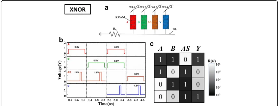
XNOR logic is widely used in constructing full adder and parity check. Circuit realization of XNOR logic op-eration is shown in Fig. 7a. Compared with circuit realization of NOR logic, an additional assistant cell marked as AS is used. Figure 7b shows the applied pulse-train waveforms. Before the operation, AS and the output cell Y are switched to HRS. The XNOR logic
Fig. 4Reliability metrics of RRAM devices.aEndurance behavior of RRAM devices.bHalf-supply voltage disturbance behavior of RRAM devices.cRetention behavior
Fig. 5NOR logic operation.aCircuit realization.bApplied pulse waveforms.cThe measured resistance truth table
[image:4.595.56.291.86.575.2] [image:4.595.302.539.88.253.2] [image:4.595.307.538.526.704.2]operation is realized by four steps. In the first step, VRis applied to A and VDD is applied to AS. This is a basic imply logic, so after step 1, AS =Ā. In the second step, VRis applied toBand VDDis applied to AS. Because AS has already been turned to Ā in the first step, so after step 2, AS is equal toA þ B. In the third step, VRis ap-plied toAandB; VDDis applied toY; this is a NOR logic operation, so the third step realized Y ¼ AþB. In the fourth step, VRis applied toAand VDDis applied toY. Be-causeYhas already turned to AþB in the third step, so after step 4,Yis equal to AþBþAþB ¼ ABþAB . Therefore, after the complete pulse train was applied, XNOR logic operation was achieved. The measured resist-ance truth table is shown in Fig. 7c, only when Aand B are in the same resistance state, then the output cell is turned to LRS, which demonstrated the XNOR logic functions correctly.
Conclusions
Logic operations including NOR and XNOR were suc-cessfully demonstrated in the ALD-fabricated RRAM crossbar arrays. Excellent performances such as large re-sistance window, uniform switching, and high reliability were achieved in the cells of this ALD-fabricated RRAM crossbar arrays, which provides opportunity for logic op-erations in the RRAM crossbar arrays.
Abbreviations
ALD:Atomic layer deposition; HRS: High-resistance state; LRS: Low-resistance state; PCB: Printed circuit board; RRAM: Resistive random access memory; VDD: Supply voltage; VR: Reference voltage; VRESET: RESET voltage; VSET: SET
voltage
Acknowledgements
This work was supported in part by the NSFC (61334007, 61421005), Beijing Municipal Science and Technology Plan Projects.
Authors’Contributions
RH carried out the measurement and analysis with the assistance of PH and drafted the manuscript under the instruction of JK, PH, LL, and XL. YZ fabricated the cross-point memory arrays with the assistance of CZ. JK supervised the work and finalized the manuscript. All authors read and approved the final manuscript.
Authors’Information
RH received his B.S. degree from the University of Electronic Science and Technology of China, Chengdu, China, in 2015. He is currently pursuing a Ph.D. degree at the Institute of Microelectronics, Peking University, Beijing, China. PH received his Ph.D. degree in microelectronics from Peking University, Beijing, China, in 2015 and B.S. degree from Xidian University, Xi’an, China, in 2010, respectively. He currently has a postdoctoral position at the Institute of Microelectronics, Peking University. YZ received her B.S. degree from Xidian University, Xi’an, China, in 2013. She is currently pursuing a Ph.D. degree at the Institute of Microelectronics, Peking University, Beijing, China. ZC received her B.S. degree from Xidian University, Xi’an, China, in 2012. She is currently pursuing a Ph.D. degree at the Institute of Microelectronics, Peking University, Beijing, China. LL received his Ph.D. degree in materials physics and chemistry from the Institute of Semiconductors, Chinese Academy of Sciences, Beijing, China, in 2005. He is currently a professor at the Institute of Microelectronics, Peking University, Beijing. XL received her Ph.D. degree in microelectronics from Peking University, Beijing, China, in 2001. She is currently a professor at the Institute of Microelectronics, Peking University. JK received his Ph.D. degree in solid-state electronics from Peking University, Beijing, China, in 1995. He is currently a professor at the Institute of Microelectronics, Peking University.
Competing Interests
The authors declare that they have no competing interests.
Received: 25 November 2016 Accepted: 23 December 2016
References
1. Lai S (2008) Non-volatile memory technologies: the quest for ever lower cost. Tech. Dig.-Int. Electron Device Meet, Washington, p 11
2. Sheu SS, Chiang PC, Lin WP, Lee HY, Chen PS, Chen YS, Wu TY, Chen FT, Su KL, Kao MJ, Cheng KH (2009) A 5ns fast write multi-level non-volatile 1 K bits RRAM memory with advance write scheme. 2009 Symposium on VLSI Circuits, Kyoto, p 82
3. Cheng CH, Tsai CY, Chin A, Yeh FS (2010) High performance ultra-low energy RRAM with good retention and endurance. Tech. Dig.-Int Electron Device Meet, San Francisco, p 19.4.1
Fig. 7XNOR logic operation.aCircuit realization.bApplied pulse waveforms.cThe measured resistance truth table
[image:5.595.55.541.88.273.2]computing. Sci Rep 14:5
9. Li H, Chen Z, Ma W, Gao B, Huang P, Liu L, Liu X, Kang J (2015) Nonvolatile logic and in situ data transfer demonstrated in crossbar resistive RAM array. IEEE Electron Device Lett 36(11):1142–5
10. Huang P, Kang J, Zhao Y, Chen S, Han R, Zhou Z, Chen Z, Ma W, Li M, Liu L, Liu X (2016) Reconfigurable nonvolatile logic operations in resistance switching crossbar array for large-scale circuits. Advanced Materials 28(44): 9758–9764
11. Govoreanu B, Kar GS, Chen YY, Paraschiv V, Kubicek S, Fantini A, Radu IP, Goux L, Clima S, Degraeve R, Jossart N (2011) 10× 10 nm 2 Hf/HfO x crossbar resistive RAM with excellent performance, reliability and low-energy operation. In Tech. Dig.-Int. Electron Device Meet, Washington, p 31.6.1
12. Waldrop MM (2016) The chips are down for Moore’s law. Nature News 11 530(7589):144
13. Chen B, Cai F, Zhou J, Ma W, Sheridan P, Lu WD (2015) Efficient in-memory computing architecture based on crossbar arrays. In Tech. Dig.-Int. Electron Device Meet, Washington, p 17.5.1
14. Li H, Li KS, Lin CH, Hsu JL, Chiu WC, Chen MC, Wu TT, Sohn J, Eryilmaz SB, Shieh JM, Yeh WK (2016) Four-layer 3D vertical RRAM integrated with FinFET as a versatile computing unit for brain-inspired cognitive information processing. In Symposium on VLSI Technology, 1-2
15. Yang JJ, Strukov DB, Stewart DR (2013) Memristive devices for computing. Nat Nanotechnol 8(1):13–24
16. Yang JJ, Williams RS (2013) Memristive devices in computing system: promises and challenges. ACM J Emerg Technol Comput Syst 9(2):11 17. Yu S, Gao B, Dai H, Sun B, Liu L, Liu X, Han R, Kang J, Yu B (2010) Improved
uniformity of resistive switching behaviors in HfO2 thin films with embedded Al layers. Electrochem Solid St 13(2):H36–8
18. Yu S, Jeyasingh R, Wu Y, Wong HS (2011) Understanding the conduction and switching mechanism of metal oxide RRAM through low frequency noise and AC conductance measurement and analysis. In Tech. Dig.-Int. Electron Device Meet, Washington, p 12.1.1
19. Chen Z, Zhang F, Chen B, Zheng Y, Gao B, Liu L, Liu X, Kang J (2015) High-performance HfO x/AlO y-based resistive switching memory cross-point array fabricated by atomic layer deposition. Nanoscale Res Lett 10(1):1 20. Chen B, Lu Y, Gao B, Fu YH, Zhang FF, Huang P, Chen YS, Liu LF, Liu XY,
Kang JF, Wang YY (2011) Physical mechanisms of endurance degradation in TMO-RRAM. In Tech. Dig.-Int. Electron Device Meet, Washington, p 12.3.1 21. Li H, Chen HY, Chen Z, Chen B, Liu R, Qiu G, Huang P, Zhang F, Jiang Z,
Gao B, Liu L (2014) Write disturb analyses on half-selected cells of cross-point RRAM arrays. IEEE International Reliability Physics Symposium, Waikoloa, p MY-3
Submit your manuscript to a
journal and benefi t from:
7Convenient online submission
7Rigorous peer review
7Immediate publication on acceptance
7Open access: articles freely available online
7High visibility within the fi eld
7Retaining the copyright to your article