© 2016, IRJET | Impact Factor value: 4.45 | ISO 9001:2008 Certified Journal
| Page 3108
Designing of Voltage Mode Universal filter Using Only Two CDBAs
Manisha Kumari
1, Ms. Rashmi kashyap
21
VLSI DESIGN, ECE Dept. & Dr. C. V. Raman University, Bilaspur, C.G., INDIA
2Assistance Professor, ECE Dept. & Dr. C. V. Raman University, Bilaspur, C.G., INDIA
---***---Abstract
- In this paper, we use a single currentdifferencing buffer amplifier (CDBA) in the current mode with application of voltage mode universal filter and all pass filter is presented. The proposed circuit is suitable for realize the proposed operation by using of two CDBA with the current processing application of filter design also we have driven the performance of CDBA. All-pass filter & Universal filter circuit was chosen as an application example in order to demonstrate the performance of the CDBA. The SPICE simulation results for frequency response as well as transient response are incorporated to verify the theory. These new configurations can realize all the five standard types of the filters, namely, low pass (LP), high pass (HP), band pass (BP), band stop (BS), and all pass (AP), from the same topology. The natural angular frequency (f), quality factor (Q) and the bandwidth (BW) parameters are also discussed. The 3dB frequency calculations are also described of all the five filters. The PSPICE simulation results are also included of all five filters. The performances of the proposed realization are shown with
the help of experimental results simulated on PSPICE. The
feasibility of the proposed work is well suited and explained with appropriate theory and simulation.
Key Words: CDBA, CMOS, CC, BW, VMUF, etc
1.INTRODUCTION
As an active building block, operational amplifier played a Predominant role in the last two decades and an enormous Number of publications exist in the literature on various circuit examples so that we can choose one of them. However, op amp-based circuits exhibit several drawbacks in their performance arising from the limited bandwidth and slew rate the feasibility The development of very large scale integration (VLSI) technology, together with the ever increasing demand for fully integrated systems containing a larger number of digital as well as analog circuits on a single chip, has ensured continued interest on analog circuit design which is required to be compatible with CMOS technology. In fact, analog circuits such as continuous- time filters, sinusoidal oscillators, digital to analog (D/A) and analog to
digital (A/D) converters, voltage comparators, current and voltage amplifiers, rectifiers, etc. are unavoidable analog circuits which cannot be realized by digital techniques. Moreover, new applications continue to appear where new analog topologies have to be designed to ensure the trade-off between speed and power requirements [1].
Analog circuit design has historically been viewed as a voltage dominated form of signal processing. Recently, current-mode analog circuits have emerged in the implementation of analog functions. In current- mode circuit description, the input and the output are both taken in the current form rather than in voltage form. In contrast to the conventional voltage mode circuits, the current mode circuits can exhibit, under certain conditions, among other things higher bandwidth and better signal linearity. Since they are designed for lower voltage swings, smaller supply voltages can be used. In addition to the advancement in current-mode analog signal processing, another particular development is the emergence of new current-mode analog building blocks among which the most prominent and popular has been the current conveyor (CC) circuit [2]. A new versatile, multi-terminal active circuit building block, current differencing buffer amplifier (CDBA) was proposed by Acar and Ozoguz in 1999.Its flexibility to operate in both voltage and current mode and low parasitic are suitable for wide band applications (Acar and Sedef, 2003), (Ozoguz, Toker and Acar, 1999), (Koksal, Oner and Sagbas, 2009), (Toker etal., 2000). It provides an attractive feature in terms of requirement of less number of passive components and better cascadability for various filter circuit and other analog signal processing circuit implementation. A number of active device are also proposed with modification of CDBA as CCCDBA, ZC-CDBA where the input port resistance is controlled by external bias current.
© 2016, IRJET | Impact Factor value: 4.45 | ISO 9001:2008 Certified Journal
| Page 3109
the all five types of filter using the Universal filter and toobtain the value of the 3 dB frequencies of the realized filters. In order to demonstrate the performances of the proposed realization, PSPICE simulation and experimental results verifying the characteristics of the designed voltage mode filters are agreed with obtained theoretical values of frequencies generation current conveyors (CCII), current-feedback op-amps (CFOA), four terminal floating nullors (FTFN), differential voltage current conveyor (DVCC), differential difference current conveyor (DDCC), third-generation current conveyor (CCIII), dual X current conveyors (DXCCII), current controlled current conveyors (CCCII) etc. received considerable attention due to their larger dynamic range and wider bandwidth. Employing these new active elements for analog design and using CMOS technology for implementation the circuit designers obtained new possibilities to solve their problems. The concept of the current conveyor was first introduced by Smith and Sedra in 1968. It was called the first-generation current conveyor (CCI) which is a 3-terminal building block device. Since then, the area of current mode circuits has progressed very fast and several thousand research papers have been published in this exciting area so far. A new active element termed as operational trans- resistance amplifier (OTRA) (commercially available as Norton amplifier 5, 44) along with its CMOS implementation was introduced by Chen, Tsao and Chen in 1992. On the other hand, another new element known as current differencing buffered amplifier (CDBA) was introduced by Acar and Ozoguz in 1999. There are numerous papers published employing CDBAs in various applications. CDBA is also known as differential current voltage conveyor (DCVC). CDBA is basically a generalization of OTRA as an universal element. Current differencing unit (CDU) and the voltage unity-gain buffer are contained into the internal structure of the CDBA. CDU is a current conveyor of the MDCC type. A Current controlled CDBA (CC-CDBA) was presented by Maheshwari and Khan in 2004. A number of active device are also proposed with modification of CDBA as CCCDBA, ZC-CDBA (Maheshwari and Khan, 2004), (Bashir and Shah, 2012).Apart from them still the work is going on to use the CDBA circuits for different low voltage and high gain applications. I have discussed some reviews of few papers concerned to floating gate device related to my project.
2. LITRECTURE SURVEY
Fırat Kaçar1, Serdar Menekay Realization of a CMOS Current Differencing Buffer Amplifier and Its Filter ApplicationIn this paper, a CMOS realization of the current Differencing buffer amplifier (CDBA) in the low voltage is presented. The circuit is suited for CMOS implementation. A first order all-pass filter circuit was chosen as an application example in order to demonstrate the performance of the CDBAA new current differencing buffer amplifier, CDBA is Presented. A new and
simple CMOS realization of this elementis given. An application example of a voltage-mode all-passfilter employing the proposed CMOS CDBA realization hasbeen presented.
Fırat KAÇAR, Yasin ÖZCELEP worked on the CDBA Based Voltage-Mode First-Order All-pass Filter Topologies with Five new configurations realizing canonical first-order voltage-mode all-pass filter configurations using a single current differencing buffer amplifier (CDBA).In this work, five CDBA based voltage-mode first order all-pass filter configurations are presented. All proposed circuits use only a single CDBA. However some of them use five passive components, some of them use four passive components. PSPICE simulations were performed with a CMOS realization of the CDBA. Simulation results show that filter characteristics are in good agreement with theory.
Gagandeep Kaur and Mohammad Ayoub Khan Second Order Multi-Mode Notch/All pass Filter using Single Current Differencing Buffered Amplifier, This worked presents a current differencing buffered amplifier as an active element for analog signal processing which support, in comparison to conventional operational amplifier not only the voltagemodeBut also the current-and mixed-mode operations. This work showed, multimode notch filter using single CDBA has been done.
Fırat KAÇAR1, Abdullah YEŞİL1 and Abbas NOORINew CMOS Realization of Voltage Differencing Buffered Amplifier and Its Biquad Filter Applications In this work, new biquad filter configuration using a recently introduced active element, namely Voltage Differencing Buffered Amplifier (VDBA), is proposed. This block has high impedance input terminals and low impedance output terminal, providing advantages at voltage mode circuit, In this work, a new CMOS implementation of voltage differencing buffer amplifier is presented and two proposed voltage-mode three-input single-output biquad filters containing two VDBAs and two or three passive components. Both filter circuits realize all filter configurations and natural frequency can be tuned electronically with bias voltage.
© 2016, IRJET | Impact Factor value: 4.45 | ISO 9001:2008 Certified Journal
| Page 3110
poly phase filter for low-IF receiver applications in this work anovel first-order active-RC poly phase filter section, using current differencing buffered amplifiers (CDBAs), is presented. The section uses 6 resistors, 2 capacitors, and 2 CDBAs. The transfer function of the proposed section has a single pole and optionally a single zero, An active poly phase filter section implemented with a CDBA was presented. It used 6 resistors, 2 capacitors, and 2 CDBAs. Although matching of the used resistors was required for the realization, this is a common feature in many circuits and can be handled easily.
J. K. Pathak1 , A. K. Singh2 , Raj Senani New Multiplier/Divider Using a Single Cdba A new multiplier-divider circuit using a single Current Differencing Buffered Amplifier (CDBA) and only six MOSFETs has been presented. The proposed circuit has the advantage of simultaneously realizing a multiplier and divider without changing the circuit topology, the presented single CDBA-based configuration uses six MOSFETs but has the advantage of realizing both multiplier and divider functions simultaneously. SPICE simulation results based on CMOS CDBA and MOS transistors in 0.35um CMOS technology.
Vishal Ramola, Saurabh Mishra Design of CCCDBA Based
Voltage Mode Differentiator and Integrator In this paper a
voltage mode differentiator (First order high pass filter) and voltage mode integrator (First order low pass filter) have been proposed by using current controlled current differencing buffered amplifier (CCCDBA) The voltage-mode building blocks of differentiators and integrators (both lossy and lossless) have been presented which can be used to form active filters. These building blocks are quite helpful in the realization of active filters for frequencies of more than 1.0MHz. These filters operate for voltage as low as 2.5V or less.
3. CIRCUIT DESCRIPTION OF CDBA
The circuit symbol of the Current Differencing Buffered Amplifier (CDBA) is shown in Fig. 1a, where p and n are input, w and z are output terminals[4]. The equivalent circuit CDBA gave blow.
Ideal current and voltage characteristics of the CDBA can be Described by Vp = 0, Vn = 0, Iz = Ip −In, Vw = Vz. (1) By taking the non-idealities of the CDBA into account, the Above terminal equations can be rewritten as Vp = 0, Vn = 0, Iz =Ip - In, Vw =Vz, Where p and n are the current gains, and # is the voltage gain. According to the equations mentioned above and equivalent circuit shown in Figure 1, the current through z-terminal is the difference of the currents through p-terminal and n-p-terminal, hence, the z-p-terminal is called current output; p- and n-terminals are non-inverting and inverting input terminals, respectively. Since the voltage at the w-terminal follows the voltage of z terminal, it is called voltage output. Note that the input terminals, through which ip and in flows, are internally grounded, where ideally the input impedance of the terminals n are internally zero[1,5].
4. CMOS RELIZATION
The proposed CDBA consists of two principal blocks: a current differencing circuit which has finite input resistances and a voltage buffer circuit. The proposed realization of the CDBA in a CMOS configuration is shown in Fig. 2.
The transistors M1 to M10 form the input stage of the CDBA element. In the current mirrors of the input stage, flipped voltage followers (FVF) [23] are used. Feedback in FVF results in very low input resistances at the input terminals. Input resistance of the p and n terminals can be given using the output resistance of FVF. In the circuit, to construct the current mirrors, outputs of FVF are used as inputs of CDBA. M2, M3and M8, M9 are FVF transistors. The flipped voltage followers, input resistances of both p and n terminals are found as 25ohm.
© 2016, IRJET | Impact Factor value: 4.45 | ISO 9001:2008 Certified Journal
| Page 3111
In this paper, the design and analysis of two newCDBA-based voltage mode universal filters (VMUFs) are proposed which not only advances the class of CDBA-based applications but also provide a number of advantages like bandwidth, gain over the previously reported filter circuits7. The 3 dB frequency analysis of designed filters is also performed. Therefore, the purpose of this paper is to realize the high performances CDBA in a different way and to offer new opportunities for analog circuit designers.
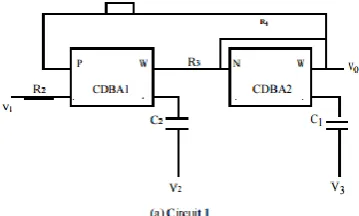
The CDBA circuit can be implemented in a number of ways. However, a popular realization based on the use of two commercially available CFOAs is shown here in Figure 3. Now the design of the universal filter using two CDBA’s is shown in the next figure.
Fig.3 Implementation of the CDBA8 using CFOAs.
[image:4.595.39.219.307.415.2]Fig.4 The proposed CDBA-based Voltage Mode Universal Filter circuit configurations.
Figure 4 shows the proposed VMUF circuits based on CDBAs. From a straight forward circuit analysis, the output voltage function, natural angular frequency (w), quality factor (Q), bandwidth (BW), gain factor, and the conditions required to realize different filters are shown in Table 1.
From Table 1, it is clear that both circuits can be used as a voltage mode three-input single-output universal filter that can realize all the standard types of filter functions. It is seen
from Table 1 that resistive matching is required to realize only band stop and all pass filters.
Both circuits enjoy tuning of filter parameters by first adjusting by 1 and/or 3 then or BW by 4 after which gain factor (in case of LP and BP) can be controlled by adjusting 2.In the proposed circuits, any additional voltage inversion is not required to realize all pass function, thus resulting in the saving of one active element.
5. Transfer function expression of Universal Filter:
To realize and analyze all five types of filter using the universal filter, first we need the transfer function expression of the universal filter. So the derivation to obtain the transfer function is given [9]
i z = I p – I n (2)
I n = V o / R ( 2 ) (3)
I z = ( V z – V 2 ) / ( 1 / C 2 S ) ( 3 )
I z = I p – I n (2)
I n = V o / R 2 (3)
I z = ( V z – V 2 ) / ( 1 / C ) 2 S )
Iz= - (Vw1/R3 + Vo/R4) Iz = (Vz – V3) / 1/SC1 Iz = (Vo –V3) / (1/SC1)
[(Vo – V3) / (1/SC1) = - (Vw1/R3 + Vo/R4)] (Vw1 – Vz) / (1/SC2) = (Vo/R1 – V1/R2) [SC1 (Vo – V3) = -(Vw1/R3 + Vo/R4)] Vw1 = (1/SC2) (Vo/R1 – V1/R2) + V2
SC1 (Vo – V3) = - [1/R3 (1/SC2(Vo/R1 – V1/R2 + V2))] SC1 (Vo-V3) = - [(1/R3SC2 (Vo/R1 – V1/R2) + V2 + Vo/R4)]
SC1 (Vo – V3) = [1/R3C2S ((VoR2 – V1R1) / R1R2) + V2 Vo/R4][- 1/R1R2R3C2S (VoR2 – V1R1) + (V2R1R2R3C2S)/R3] + [Vo/R4- Vo/R1R3C2S + V1/R2R3C2S –V2/R3 – Vo/R4]
[image:4.595.40.229.482.603.2]© 2016, IRJET | Impact Factor value: 4.45 | ISO 9001:2008 Certified Journal
| Page 3112
V3SC1]Vo [(SSC1C2R1R3R4 + R4 R1R3C2S) / R1R4] = (V1 – V2R2C2S + V3SSC1C2R2R3) / R2 Vo C1C2R1R3 / R1R4 [SS + (R1R3C2S/C1C2R1R3) + (R4/R1R3C1C2)]
Vo = [1/R2 (V3SSC1C2R2R3 – V2SR2C2 + V1)] / [C1C2R3/R4 (SS + S/R4C1 + R4/R1R3C1C2)] Vo = [C1C2R4 (V3SS – V2S/C1 + V1/R1R3C1C2)] / [SS + S/C1 + R4/R1R3C1C2]
Vo = (V3SS – V2S/C1 + V1/R1R3C1C2) / (SS + S/C1R4 +
1 / R 1 R 3 C 1 C 2 ) ( 4 )
In this paper, the 3-dB frequency of every filter is also calculated with the help of the results simulated on PSpice software. All the proposed filters using universal filter have also their 3 dB frequency calculations, which is presented with their respected filters.
6
. Simulation and Results:
To conserve space, the simulation results of only Circuit 1 of Figure 4 are presented with passive components values chosen as 𝐶1 = 𝐶2 = 100 pF (in all responses), 𝑅1 = 1.59 kΩ (LP, HP, BP, BS), 𝑅1 = 4.75 kΩ (AP), 𝑅2 = 1 kΩ (LP, HP, BP), 𝑅2 = 1.75 kΩ (BS), 𝑅2 =4.9 kΩ (AP), 𝑅3 = 1.59 kΩ (in all responses), 𝑅4 = 1.12 kΩ (LP, HP), 𝑅4 = 1.59 kΩ (BP, AP), and 𝑅4 = 1.43 kΩ (BS). The simulation results, thus, confirm
the validity of the theoretical formulations. The PSpice simulated waveforms of the CDBA circuit and the response of all filters implemented using the universal filter are also presented in this section and the value of the 3dB frequency are also evaluated using the PSpice simulated results.
[image:5.595.306.508.134.250.2]The Low Pass Filter: The simulated result on PSpice for Low Pass Filter is shown in figure:
Fig : 5 low pass filter
The 3dB frequency or the cut off frequency of the above Low pass filter, obtained from the graph is 73.555MHz.
The High Pass Filter:
[image:5.595.307.509.421.534.2]The simulated result on PSpice for High Pass Filter is shown in figure:
Fig.7 The response of HPF obtained using universal filter. (The gain Vs frequency)
The 3dB frequency or the cut off frequency of the above High pass filter, obtained from the graph is 33.913GHz.
The Band Pass Filter:
The simulated result on PSpice for Band Pass Filter is shown in figure:
[image:5.595.36.236.554.670.2]© 2016, IRJET | Impact Factor value: 4.45 | ISO 9001:2008 Certified Journal
| Page 3113
The 3dB bandwidth BW = f2 − f1, where f1 is lower cut offfrequency and f2 is the higher cut off frequency. So from the above graph …. The centre frequency of this filter is 1.9953GHz. And f1=420.182MHz and f2=18.541GHz, so 3dB Bandwidth of the above designed Band Pass Filter is 18.120GHz.
The Band (Stop) Reject Filter:
The simulated result on PSpice for Band Reject Filter is shown in figure:
Fig.9 The response of HPF obtained using universal filter. (The gain Vs frequency)
From the above Band Reject filter graph, we obtained…. The Lower cut off frequency (f1) =1.2580GHz. The Higher cut off frequency (f2) =3.6915GHz. The center frequency is 1.9953GHz. So the 3dB bandwidth of this filter is given by= f2-f1. The 3 dB bandwidth of the filter is 2.4335 GHz.
All Pass Filter:
It is a signal processing filter that passes all frequencies
equally in gain, but changes the phase relationship between
various frequencies. It does this by varying its phase shift as
a function of frequency. Generally, the filter is described by
the frequency at which the phase shift crosses 90° (i.e., when
the input and output signals go into quadrature – when there
is a quarter wavelength of delay between them). They are
generally used to compensate for other undesired phase shifts that arise in the system, or for mixing with an
unshifted version of the original to implement a notch comb
filter. They may also be used to convert a mixed phase filter
into a minimum phase filter with an equivalent magnitude
response or an unstable filter into a stable filter with an equivalent magnitude response. C1= C2 =100Pf, R1 = 4.75K, R2=4.9K, R3 =1.59K, R4 =1.59K.
Fig.10 The response of APF obtained using universal filter. (The gain Vs frequency)
To verify the performances of the proposed CDBA based universal filter, the response of all five type filters are shown in Fig. 6, Fig. 7, Fig.8, Fig.9 were simulated with the same circuit parameters using PSPICE simulation and the frequency is obtained. From the above experimental results of the filters, one can verify that the proposed CDBA can be seen as suitable to offer new opportunities for analog circuit designers in future..
7.Conclusion
The proposed voltage mode universal filter is implemented using two CDBA’s. And the response of all the five filters (LP, HP, BP, BR, AP) are also discussed in detail using the universal filter. This work covers new advances and possibilities in the relate research area including application on communication, measurement and RF systems. Employing these new active elements for analog applications and using CMOS technology for implementation, the circuit designers obtained new possibilities to replace the conventional operational amplifier in their design to solve the problems. This paper also presents a little review on the current status and the recent development of the current differencing buffer amplifier. The results of various reviewed papers explore and confirm the applicability of CDBA in analog signal processing circuits.
REFRENCES
[1]. Sachin Kumar Rajput and Anu Mehra, “Comparative Analysisof Current Differencing Buffer Amplifiers”, ARPN Journal of Engineering and Applied Sciences. VOL. 10, NO. 16, SEPTEMBER 2015.
[2]. H. Hakan Kuntman, “New Advances and Possibilities Provided By Alternative Active Elements in Analogue Circuit Design”. Firat University.
[3]. Jitendra Mohan, Bhartendu Chaturvedi. I.J. Image, “Novel Current-Mode All-Pass Filter with Minimum Component Count”, Graphics and Signal Processing, 2013, 12, 32-37, October 2013 in MECS.
© 2016, IRJET | Impact Factor value: 4.45 | ISO 9001:2008 Certified Journal
| Page 3114
differencing buffered amplifier suitable for analog signalprocessing filters”, Microelectronics J.,Vol. 30, pp. 157-160, 1999. [5]. Ali Ümit Keskin, Dalibor Biolek, Mehmet Said Yükselten, “Current Mode Multifunction Biquad Using Single CDBA” Istanbul Turkey.
[6]. Ali Ümit Keskin and Erhan Hancioglu, “CDBABased Synthetic
Floating inductance with Electronic
tuningProperties”.International Journal of Electronics, vol. 92, no. 8, pp. 479–487, 2005.
[7]. Ersin Alaybeyoğlu, Arda Güney, Mustafa Altun and Hakan Kuntman, “Design of Positive Feedback Driven Current-Mode Amplifiers ZCopy CDBA and CDTA, and Filter Applications”. [8]. S. Ozouguz, A. Toker and C. Acar, “Current-mode continuous-time fully integrated universal filter using CDBAs”, Electronics Letters, Vol. 35, No. 2, Pp. 97-98,Jan. 1999.
[9]. Book “Design of Analog Filter” by Rolf Schaumann and Mac E. VanValkenburg.