United States Patent
Levy et al.
[ 19]
[54] SECONDARY STORAGE FACILITY FOR DATA PROCESSING SYSTEMS
[75] Inventors: john V. Levy, Maynard; Steven R. jenkins, Medford; Victor Ku, Westboro; Peter McLean, Stow; Thomas N. Hastings, Arlington, all of Mass.
[73] Assignee: Digital Equipment Corporation, Maynard, Mass.
[22] Filed: jan. 10, 1974 121] App!. No.: 432,140
144 J Published under the second Trial Voluntary Protest Program on March 23, 1976 as document No. B 432,140.
[52] U.S. CI ... 340/172.5 [5 I] Int. CJ.2 ... G06F 3/00 [58J Field of Search ... 340/172.5 [561 References Cited
3.61 S.041 3,623,022 3,643.223
S y S
T
E
M
8
U
5
UNITED STATES PATENTS
11/1971 11/1971 2/1972
Horikoshi ... 340/172.5 Dayc ... 340/172.5 Ruth ct al ... 340/172.5
READ
3.699,532 3.742,457 3.760,364 3.766,526 3.810,105 3,828,325
10/1972 6/1973 9/1973 10/1973 5/1974 8/1974
[11] B
3,999,163
[45]
Dec. 21, 1976
Schaffer et al. ... 340/172.5 Calle ct al. ... 340/172.5 Yamauchi ct al. ... 340/172.5 Buchanan ... 340/172.5 England ... 340/ I 72.5 Stafford et al. .... 340/1 72.5
Primary Examiner-Charles E. Atkinson Attorney, Agent, or Firm-Cesari and McKenna
[57] ABSTRACT
A secondary storage facility including magnetic tape, disk or drum units or other sequential access storage units. Each storage unit or drive connects to a control-ler by means of a device bus with asynchronous and synchronous paths. Status and controller information is coupled between the controller and a selected drive unit asynchronously over the asynchronous bus. Actual data transfers occur between the controller and a drive over the synchronous bus and between other units in the system and the controller using direct memory access or equivalent data transfers.
32 Claims, 21 DrawinK Figures
121
280
u.s.
Patent
Dec. 21, 1976
Sheet 1 of 19
3,999,163
MAIN
MEMORY
UNIT
C:I
..
-••
CONTROLLER
I}
r~
DRIVE
\
1oooo--_L"'~l
"r
22
~
rf:::/
I
DRIVE
'--_ _
L
...
~
DRIVE
I
-CPU
.~
h
r
~13
..
-
CONTROLLER
23~
V-
24
I I
I I
DRIVE
DRIVE
--25
37
u.s.
Patent
Dec. 21, 1976
TELETYPE-
.-/
WRITER
L>--.-CARD
1---4INPUT-OUTPUT
BUS 36
1Sheet 2 of 19
3,999,163
CPU
~_:J
CORE
31
--1r=t==:::I:J
MEMORY
J-.-
AMEMORY'
BUS
30
:J
32
/
READER
L --.~40 ' - - - '
PAPER
r
I---<TAPE
/
PUNCH
'-1--4~---.
41
'---~';;';";""'--I;::='.:J
CORE
DRIVE
42
~
______
~CONTROLLER~~~~~t~=G;~'
__
M~~~~~R_Y~
45
I_ _
46
DRIVE
r~43
'-I-
FIG.2
DRIVE
[
f--44
--k
/ 5 2
....
/51
~~
-.
MEMORY
FAST
INPUT-
CPU
Y
34
OUTPUT
Ir-PUT -OUTPUT
50
MEMORY
DEVICES
"-
JBUS
\.. )BUS
\.53
y y
v
I~UT
-OUTPUT
PROCESSOR
MEMORY
SECTION
SECTION
SECTION
u.s.
Patent
Dec. 21, 1976
Sheet 3 of 19
/
FAST
MEMORY
UNIT
CPU
...-_..1&--_ _
)5
MAIN
MEMORY
UNIT
~::;/;::::::==~-
---=>
CONTROLLER
l61
3,999,163
CONTROLLER
DRIVE
_ _
63
1/0
DEVICES
/68
~
.--__ ...
DRIVE
(62
66
~69
DRIVE
FIG. 3
[image:4.612.109.550.99.674.2]u.s.
Patent
Dec. 21, 1976
Sheet 4 of 19
3,999,163
FIG.4
80
CONTROL SECTION 80
CONTROL DATA(CD)
84 }
DATA SET 81
--..- PARITY (CPA)
85
DS
86 }
ADDRESS SET
82
RS
87
OEM
91
TRA
92
ATTN
94
INIT
95
CONTROL SET
83
- -
- - - ---
- - - -
-DATA SECTION
100
103
DATA PARITY (DPA)
DATA
}DATA SET 101
CONTROL SET 104
110
\.
v
)
'---v---~-----
l"---_--.. _____
-
~J
CONTROLLER DRIVE
B
U
S
>
_BUS
iAt>DRESS
....
!RECEIVERS/
1
r295
r'DRIVERS
v
R;2-0---FIG.5
137
WRITE-CHECK
~
~~81~~l~
II
~
L /
J
READ
WRITE CHECK
124?
II
ClK OBUF
OUTPUT ...
BUFFER
STORAGE
FACILITY
[l
c:
299
WRITE-CHECK
ERROR
...
p97
WRITE
-DRIVERS _
--
~
291
174
DRIVE WORD
COUNTER
REGISTER
294
WORD
COUNTER
REG ISTER
1-136
L.INTERRUPT
121/
(280
....
---WRITE
,RECEIVERS. 101
L
~
~
c
.
CI'J
.
~
~
!""fo.
(D
='
!""fo.
o
~
N
...
~
...
~
0'1
t.I.l
::r
o
o
...
VI
o
......
\0
w
...
\0
\0
\0
...
1-100\
, 166\..
BUS
I
I
FIG.6
16~
MUX MUX~70
MUXV
l72c;:::: DRIVERS
V
l62
100~
116~ (6~
17~
(~
'1• f
f •
_CDout CSlouUBAout OB out
CS20ut ~
~ WCout
I
RECEIVERS""
OUTPUT 13[ BUFFER ... 124~}
BUS WORD
V
l36CONTROL CONTROL
-
I~ UNIT j . )
ADDRESS COUNTER
133 ...
a
EllO~D54
REGISTER REGISTER STORAGE123 STATUS STATUS -- SELECT CO, FACILITY
REGISTER REGISTER CPA S
..----t
1-134Y
T l
I--WCin
Vl22
S BAin GATING
CS}in
~
CIRCUI1I-- REG INPUTCSI in---1
T
REG STRE
( STR BUFFER M
173
-ORin
t
I·{:DRIVERS I--e
~ RECEIVERS/
L
DRIVE 1---174 1547
lREG STRB
DRIVERSU WORD
I-I~
IS COUNTER
,.120
r---+REG STR
156 156 156 156 156
-121../
15~
TIMING....
"- TRANSFER~
CIRCUIT TRA...,.-v
CONTROL'""!:
ADDRESS DEV SEt...~ TIMINI~
I
CIRCUI
~
161
ADDRESS VALIDL
~
I
(
CTODI ~WC in/out
...
ADDRESSf
~
CIRCUIT DIRECTION REGISTER-BA in/out
--
~
...
CONTROL SELECTION
f--.
CS II n / outUNIT _J'...
~
LOCAL DECODER ~ CS2 in/out
160 ... DEVICE
SELECT~
OUTPUT~
152f--t.
OB In/outBUS
f----v'
I
r==--'
I--
CD In/out CONTROL -C-RS'" DRIVERS OEM _ ~n
/151I
RS'J- - - - -
176 - - - - ,0 5 - 1..1
RS - - - t - - l
DEM---~1--i~~~~~
rRA-I N rRA-I
r_.a--+..
CTOD
CD.. 1 1_
I
I
I
145')
I
CPA· I
~
1 .. 1ATTN.... L, 121
o
--r--t---.DPA
1"'--EBl
I
RUN _ _ 107
"t;ll
S----
iS CLK
oce
l6
1
/,1
I
I
1121
I
,-~
_ _ _ _ _ _ _ _
.J
DRIVE CONTROL
CIRCUIT
62
FIG.7
DRIVE TRANSPORT
B
MEDIUM
263
c
.
c.n
.
~
e
('1)
::s
f"'+-o
(lj
P
tv
..-~
..-\0 -.l
0'1
en
:r
(lj (lj
...
-.l
o
....,
..-\0
w
...
\0
\0
\0
...
,...
0'\
u.s.
Patent
Dec. 21, 1976
Sheet 8 of 19
3,999,163
CONTROLLER
DRIVE
200
v
210
NEGATE OEM
214
215
A
CTODB
os
ASC
CD } CPAD
OEME
TRAF OS }
c'50
G
CO CPAH OEM
I
TRAA
CTOD B RS osC
CD 15 CPADOEI.'
E TRA
F cO CPA
G
OEM H TRAU.S. Patent
Dec. 21, 1976
Sheet 9 of 19
3,999,163
. . . - - SELECT LINES VALID - - - t ; NEXT
CYCLE-L
ONTROLLER
DRIVE
t
t9
FIG.9
ta
~gat-.
--NEXTCYCLE-~Ie-'
- - S E L E C T LINES VALID----~/-I--.
--NEXTCYCLE-_1-.
--CONTROL LINES VALID---1.~{%;;f--NEXTCYCLE-t
4
f
FIG. II
I
t
f
6
ONTROLLER
[image:10.612.95.558.78.734.2]u.s.
Patent
Dec. 21, 1976
Y
CONTROLLER
ASSEIHCTOO GENERATE CPA
227
Sheet 10 of 19
3,999,163
DRIVE
FIG. 10
231
GATE IN ~~A ASSERT TRA
GATE Chny tnltll INTO A T A RESET
N
[image:11.612.125.515.111.702.2]U.S. Patent
Dec. 21.1976
Sheet 11 of 19
3,999,163
CONTROL S STATUS
REGISTER 140
STATUS
REGISTER 141
ERROR
REGISTER 142
MAINTENANCE
REGISTER 144
ATTENTION
SUM-MARY REGISTER 145
DESIRED TRACK
SECTOR
REGISTER 146
DRIVE TYPE
REGISTER 147+
LOOK AHEAD
REGISTER 148+
SERIAL NUMBER
REGISTER 250
ECC POSITION
REGIST ER 251
ECC PATTERN
REGISTER 252
OFFSET
REGISTER 253
DESIRED CYLINDER
~~RESSREGISTER
DRIVE REGISTER
[---
-'
I OVAl
- - - -
I
FUNCTION
I
GO]
-+
IATAIERRI PIP IMOQNRLbBTI
I
IORyl-
=-
-=-=-
~_~~_
~_
-=--=J
IDCKIUN~OPIIDTEtM-EILAEI
AO
I
- - - -
- - - - -
IPAffMRllLRllFEI
+
... ++
-===
==--~=--=--=lQf!1~
I8LFkI
OPTION
Ispi
C--=---==--=--=--==--=--==-- FTf
IAtAI
A!AIA~A
IA!A I A!AI ATAIATtJ
[
-I
TRACK ADDRESS
I
SECTOR
ADDRESS
~
-f\JsA/ T@M§H7CHIDRQ!SPR!
I
DRIVE I D
I
r
-I
CURRENT SECTOR
I
SECTOR FRACTION!
L _ _ _
I
DRIVE SERIAL NUMBER
]
r---~
L _ _ _ _ _ _ _ _ _ _ _ _ _ _ _ _ _ _ _ _ _ _ _ J
, - - - ,
L _ _ _ _ _ _ _ _ _ _ _ _ _ _ _ _ _ _ _ _ _ _ J~
_____
OF_F_SE_T
____
---~-J
CYLINDER ADDRESS
~~~~~1 ~!~II~~~~~~I
_ _ _ _ _ _
C_U_RR_E_N_T_A_R_M_A_D_D_RE_s_s _ _ _ _ _
---'
255
v
FIG.13
CONTROL REGISTER
CONTROL AND STAT-I sc ITREI
Me
I
US REGISTER 133
P E+
I
~f
IAI71A 16IRDyII E
I
---~ _ _ _ _ _ _ ..J
+
+
+ + + ++ +
WORD COUNT
REGISTER 136
BUS ADDRESS
REGISTER 137
WORD COUNT
SYSTEM BUS ADDRESS
u.s.
Patent
Dec. 21, 1976
Sheet 12 of 19
3,999,163
A
CTOOBRS
J,..---REGISTER SELECT:04
a
C
co
0
CPA·.j}::¥{};J%%E~&diENEXT
CYCLEE
OEM--~II
~
______ __
ONTROLLER
F
TRArq
! IG
RSDRIVE
H
CO / / -r~ CONTROL LINE VALID ----eo[/'I
OEMJ
TRAf f
f
f
f
f
Ht
I II I
1
~19
u.s.
Patent
Dec. 21, 1976
Sheet 13 of 19
3,999,163
NEXT CYCLE
CON-~ _ _ _ _ _ _ TROLLER
t
t t
t
'5 ..
...
'6
FIG. 15
L
l ... I __
Jf t
t
t
t
a ' ... .,
[image:14.612.122.555.205.630.2]u.s.
Patent
Dec. 21, 1976
Sheet 14 of 19
3,999,163
CONTROLLER
DRIVE
254
252
ASSERT RUN261
OPERATION INCOMPLETE"
285
NEGATE EBl
286
290
U.S. Patent
Dec. 21, 1976
Sheet 15 of 19
3,999,163
CONTROLLER
f
f
-I -I I I I
I
I ~ _ _ _ .!. ____ .!. ____ .!. _____ L.... _ _ _ _ _ _ _ 1
I I I I
B RUN (C)(T) _ _ ....J
c
EBl (C)(R) _ _ _ _ _ _ _ _ _ _ _ ---+----~--_<_~o
SClK (C )(R) _ _ _ _ _ _ _ _ ..J~~~
WORD I 'WORD 2 , WORD 3 WORD 4f RUN (OIlR)
G
EBl (O)(T)L
DRIVE
H SClK IOI{T)
t
I
t
2t
3t
411
6t1
7tt
6 7tt
~t
6 7tt
H
6f!
7 10t
11t
12 13t t t
14 [image:16.612.91.551.236.630.2]u.s.
Patent
Dec. 21, 1976
Sheet 16 of 19
3,999,163
CONTROLLER
DRIVE
312
I
ERROR CLASS B
)
310
"OPERATIONv INCOMPLETE""
313
314
316
FIG. 18
311
324
[image:17.612.102.541.97.706.2]u.s.
Patent
Dec. 21, 1976
Sheet 17 of 19
3,999,163
CONTROLLER
.
WORD 1 WORD 2
I
WORD 3I
WORD 4~
I I I
I I I 1
I I , , ,
I
' j I t
: ' - - - ' - - - !....- - - ' - - - - '
-I I I I
I I I :
r---: : 1
I
I I I .
B
RUN (CUTIC EBl (C}(R)
I I I I
0
SClK (CURl__________
~rl
~~
_____ _
E WClK (CIITI
__________
~Il
~~
____ _
F D (O:17} (DlIR)
DPA
~
•
•
I•
G
RUN (oliRI
H EBl (o1IT!
l
I
SClK (ollT)
I
J
WClK (ollR)________
~Il ~~~~
DRIVE
t
11
2 3t
[image:18.612.106.555.229.693.2]u.s.
Patent
Dec. 21, 1976
Sheet 18 of 19
3,999,163
371
I~SHIFT
ClK
IBUF
(+1)-0
~~
WRCHK
j372
BUB
FUNCTION
~Cl~
37
1
FUNCTION
...DECODING
•
.;
CIRCUIT
361
WRC,
~ 1IBUF
11"36.§.J367
0-
o
S
READ
FUll
350
.w
ITE
1\
~
3~
IBUF
8
---
FUll
FUNC.
I
i
3
IR
..
g-c
R
bJ.r370
ClK
1
374
C~K
DATA
~J357)
SILO
WCLK
(+0-0
36
91
S
10~
v-353
~-FUNC
lOAD
SClK
~
C R
105..:.)
DEV
~
SEl
GO
~
CSlin
363
INH
DRWC OFlO
~365
(355
START
RUN
OBUF FUll
~
(+/)-0
RUN
r
390
~C
....
o '
EOS
4
J
,.--
C
TRE
" I
)-I
J35~
~
NED
--r
!¥391
III---=-";
EXC
ClR
38
EBl
ERROR
1I0----.J
RDY----~
RWRCj
'
-
WRITE---~NED
MXF
U.S. Patent
Dec. 21, 1976
CLK
GLCR
SCLR
MXF
EOS
CLR SILO
WCOFLO
CLR
OR
aBOUT
CLK OB
WRITE
S CLK
CLK DATA
RWRC
394
(0)
WR CHK ERROR
OBUF FULL
D
S
a
D S
OBUF
BUB
FULL
OUT
376
378
C
R
C
FIG.208
Sheet 19 of 19
3,999,163
417
412
(I)
D
MXF
FF
MXF
C
CLR
OCC
112
418
D
386
C
1
3,999,163
2
SECONDARY STORAGE FACILITY FOR DATA PROCESSING SYSTEMS
BACKGROUND OF THE INVENTION This invention generally relates to data processing systems and more specifically to secondary storage facilities connected in such systems.
Secondary storage facilities comprise elements which are not an integral part of a central processing unit and its random access memory clement, but which are di-rcctly connected to and controlled by the central pro-cessing unit or other elements in the system. These facilities are also known as "mass storage" elements and include magnetic tape memory units, disk units and drum units.
These facilities are also termed "sequential access storage units" because the information stored in one of these units becomes available, or is stored, only in a "one-after-the-other" sequence, whether or not all the information or only some of it is desired. For example, it is usual practice to retrieve information from a disk unit on a "sector-by-sector" basis, even though only one of several information records in a sector is needed. Similarly, a physical record on a tape is analo-gous to a sector on a disk and a complete physical record may be retrieved even though it may contain more than one relevant information record.
for that system in conjunction with the new tape drive. Rather, it was necessary to design a new magnetic tape drive con troller.
This procedure, of course, led to duplications of 5 engineering effort, even when the same manufacturer introduced new drives or data processing systems. En-tirely new secondary storage facilities were usually developed. The uniqueness of each of the drives and controllers also led to user problems. If a user already
10 had a system, he often had to replace both drives and controllers to obtain the benefits of a new drive. Fur-thermore, a controller was adapted to operate with one type of drive, so it was not possible to intermix the same types of drives (e.g., different disk drives) on one con-15 troller. This sometimes necessitated a different control-ler for each drive even though neither controlcontrol-ler was
used to capacity. .
Therefore, it is an object of this invention to improve the operation of a secondary storage facility including a 20 controller and a drive.
Another object of this inventiorl is to provide such a facility in which the drive design is independent of a particular controller or data processing system.
Still another object of this invention is to provide 25 such a facility in which the controller design and
opera-tion are independent of the controlled drive.
These devices are also "serial storage devices". In a serial storage device time and sequential position are 30 factors used to locate any given bit, character, word or groups of words appearing one after the other in time sequence. The individual bits appear or are read seri-'lily in time.
Yet another object of this invention is to provide such a facility in which a single controller can control different types of drives.
Still yet another object of this invention is to provide such a facility in which a single drive can be used with different kinds of data processing systems.
SUMMARY OF THE INVENTION In modern data processing systems a secondary stor- 35
age facility includes a controller and one or more drives connected thereto. The controller operates in response
In accordance with this invention, two distinct paths interconnect a controller and drive. One is an asyn-chronous drive control path including data, address and control lines. The signals over this path perform control functions and include control signals for effect-ing information transfers to or from addressed storage locations in the drive. The starting address in the drive to signals from the data processing system, usually on
an input/output bus which connects together other elements in the system including the central processing 40 unit. A drive contains the recording medium (e.g., tape or a rotating disk), the mechanism for moving the me-dium, and electronic circuitry to read data from or store data on the medium and also to convert the data between serial and parallel formats.
The controller appears to the rest of the system as any other system element on the input/output bus. It receives commands over the bus which include com-mand information about the operation to be per-formed, the drive to be used, the size of the transfer, the starting address on the drive for the transfer, and the starting address in some other system element, sueh as a random access memory unit. The controller con-verts all this command information into the necessary signals to effect the transfer between the appropriate drive and other system element. During the transfer itself, the controller routes the data to or from the appropriate drive and from or to the input/output bus or a memory bus.
In prior systems, each secondary storage facility was unique. That is, a controller was designed to link a specific drive to a specific data processing system and a drive was designed to be connected to a specific con-troller. If a new drive was developed, a new controller was also developed. This was especially true if the new drive was a different type of drive. For example, if a new magnetic tape drive was developed for a system, it was not possible to use an existing disk drive controller
and the size of the transfer are typical items of informa-tion which are sent to the drive over this path.
The second path is a synchronous data path which 45 transfers the data itself. It contains data and control lines. The control lines carry signals used for synchro-nizing the controller and drive, starting a data transfer and signalling any malfunctions which might occur during the transfer.
50 The signals on these two paths constitute a standard set of signals which can control disk drives, magnetic tape drives, magnetic drum drives and other sequential access or serial storage devices. ]f a system contains a controller constructed in accordance with this inven-55 tion, then any drive which is constructed in accordance
with this invention can be interchanged without alter-ing the controller. Further, a set of these drives can be connected to another type of data processing system just by changing only a part of the controller. No 60 changes are necessary to the drives. ]n fact, if the new data processing system already has a controller con-structed in accordance with this invention. then drives from the former system can be connected without any further alterations. Thus, a controller is independent of 65 the drive it controls and the drive is independent of the
controller and system to which it connects.
3
3,999,163
4
advantages of this invention may be attained byrefer-ring to the following description taken in conjunction with the accompanying drawings.
BRlEF DESCRIPTION OF THE DRA WINOS FlO. 1 is a generalized block diagram of a data pro-cessing system adapted to use this invention;
flO. 2 is a block diagram of one type of data process-ing system shown in FlO. 1 in which separate memory and input/output buses link elements in the system;
FlO. 3 is a block diagram of another type of data processing system shown in FlO. 1 in which a single bus is common to all elements in the system;
FlO. 4 depicts an interconnecting bus between a drive and controller in accordance with this invention. flO. 5 is a block diagram of a synchronous data path in the controller as adapted for connection to a system as shown in FlOS. 2 or 3;
FlO. 6 is a block diagram of an asynchronous drive control path in a controller as adapted for connection to a system as shown in FIOS. 2 or 3;
FlO. 7 is a block diagram of a drive constructed in accordance with this invention;
flO. 8 is a flow chart of the operation for retrieving information in a register shown in flO. 7;
FlO. 9 includes timing charts corresponding to flO. 8;
flO. 10 is a flow chart of the operation for storing information in a register shown in FlO. 7;
ory unit, a magnetic drum memory unit or a magnetic tape unit, as well as non-mechanically driven memory units. Timing signals derived from the medium nor-mally synchronize data transfers with movement of the 5 medium. A typical drive contains control, status, error and other registers for controlling and monitoring drive operations.
A controller 13 or 16 may be located physically sepa-rately from the central processing unit 10 as shown in 10 FlO. 1 or may be an integral part of a central
process-ing unit. Controllers serve as "interfaces" between the central processing unit and the drive. They contain the circuits for exchanging data with either the central processing unit 10 or the main memory unit 11. Buffer 15 registers in the controller 13 or 16 compensate for the usually different transfer rates between the controller and main memory unit 11, on the one hand, and be-tween the controller and drive, on the other hand.
Drives are connected to controllers by means of de-20 vice buses in several different configurations. If, for
example, the controller 16 were connected to drive 17 only, the arrangement would be termed a "single drive" configuration. Actually, as shown in flO. 1, the drives 17, 20 and 21 are interconnected by a device bus 25 22 which is threaded from one drive to the next. This is an example of a "daisy-chain" configuration. Device buses 23 and 24 connect drives 14 and 15, respectively, in a "radial" configuration. Drive 14 is linked to the
FlO. 11 includes timing charts corresponding to flO. 30 10;
controller 16 by way of a device bus 25; the drive 14 is thus in a "dual controller-single drive" configuration.
It will become apparent from the following discussion that this invention is adapted for all these configura-tions. The user of a system will determine his own spe-cific configuration. It also will become apparent that if flO. 12 depicts the organization of registers adapted
for use in a controller;
flO. 13 depicts the organization of registers adapted for use in a drive;
FlO. 14 includes timing charts for retrieving informa-tion from a specific register;
FlO. 15 includes timing charts for storing informa-tion in a specific register;
35 drive 14 is one type of magnetic disk memory unit, drive 15 can be another unit of the same type, a netic disk memory unit of another type, or even a mag-netic tape or magmag-netic drum unit or other type of
se-flO. 16 is a flow chart of the operation of a controller 40 and drive to retrieve data from the drive;
quential access memory. Moreover, drives 17,20 and 21 could be directly connected to controller 13 without any modification to either the controller 13 or any of flO. 17 includes timing charts corresponding to FlO.
16·
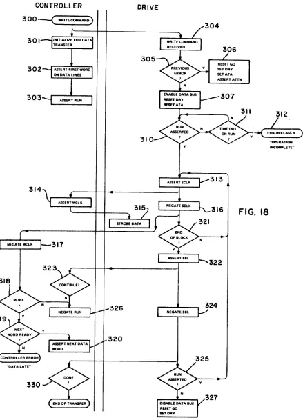
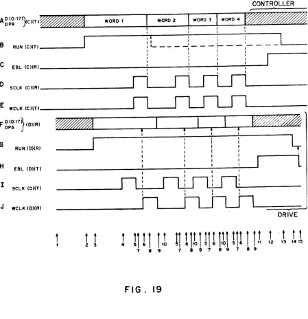
FlO. 18 is a flow chart of the operation of a controller and device bus to store data in the drive;
FlO. 19 includes timing charts corresponding to FlO. 18; and
FIOS. 20A and 20B arc detailed circuit diagrams of control circuits shown in FlO. 5.
DESCRIPTION OF ILLUSTRATIVE EMBODIMENTS
I. Oeneral Description
FlO. 1 depicts the general organization of a data processing system comprising a central processing unit (CPU) 10 and a main memory unit 11, normally a random access memory unit. Information also may be transferred to or from a secondary storage facility in-cluding a controller 13 and several drives, drives 14 and 15 being shown by way of example. Another such storage facility includes a controller 16 and drives 17, 20 and 21. This facility is also coupled to the central processing unit 10 and the main memory unit 11.
the drives.
This interchangeability and resultant flexibility result because each of the device buses 22, 23, 24 and 25 45 contains a standard set of corresponding conductors for transferring signals according to this invention, notwithstanding the drive connected to the device bus or the data processing system which is involved. As new drives are developed with improved storage media such 50 as tapes and disks with higher recording density or even of new media, it will only be necessary to have the drive itself conform to the standard set of signals, no new controller development will be necessary.
New drives will also be independent of the type of 55 data processing systems to which they connect. FIOS. 2 and 3 depict diverse types of data processing systems. The nature of the data processing system has no effect on the drive itself. Although these two data processing systems form no part of the invention, the fact that they 60 are diverse types of systems emphasizes the flexibility that this invention provides to secondary storage facili-ties. Also, specific examples of data processing systems will facilitate an understanding of the detailed discus-As previously indicated, a "drive" includes a
record-ing medium and the mechanical and electrical compo- 65 nents for recording data on or reading from the record-ing medium in the context of this invention. For exam-ple, it can comprise a fixed or movable head disk
mem-sion of this invention.
5
3,999,163
6
(CPU) 31 with a memory section including, forexam-ple, a core memory 32, a core memory 33 and a fast or volatile memory 34. An input-output bus 36 connects the central processing unit 31 with several input-output devices such as a teletypewriter 37, a card reader 40, and a paper tape punch 41. The memory bus 30 and the input-output bus 36 carry control, address and data signals in two directions. The signals on each bus are transferred in parallel, as distinguished from serial transmission.
The central processing unit 31 can also control the transfer of data between the memory section and a secondary storage facility. In FIG. 2 this storage facility comprises drives 42, 43 and 44 connected to a control-ler 45 by a device bus 46 in a daisy-chain configuration. In accordance with this invention, the controller 45 receives control information over the input-output bus 36 to be processed by an asynchronous drive control path within the controller 45. A synchronous data path in the controller may transfer data to the memory bus 30 or, as shown. to a second memory bus 47. Thus. transfers between the secondary storage facility and the memory section occur only with minimum use of the input-output bus 36 and the central processing unit 31 because data can be transferred directly through the controller 45 to the memory section. As also shown in FIG. 2 a second central processing unit 50 connects through an input-output bus 51 to other input-output devices 52. The central processing unit 50 also con-nects to the memory section through a bus 53, which enables the unit 50 to use the memory units 32, 33 and 34 in common with the processing unit 31 including data supplied to the memory section by the secondary storage facility.
As previously stated. this is an example of a data processing system which has separate input-output and memory buses. In operation. the central processing unit 31 might require some program stored in the drive 42. A second program already stored in the memory sec-tion would contain the necessary instrucsec-tions to trans-fer a command to the controller 45 over the bus 36 to identify a particular drive. such as the drive 42, the starting location in the drive (e.g., the track and sector numbers in a disk memory unit) and other necessary information. as known in the art. Once the controller 45 receives that information, it retrieves data from the drive 42 and then transfers it to the memory bus 47 directly for storage and subsequent use by the central processing unit 31 or even the central processing unit 50.
Analagous transfers occur in a system using a com-mon bus to interconnect the system elements. Such a system is shown in FIG. 3 and comprises a central pro-cessing unit (CPU) 60 and a first common bus 61. The bus 61 contains address, data and control conductors.
It connects the central processing unit 60 in parallel with input-output devices 62 and controllers 63 and 64 associated with two secondary storage facilities.
The controller 63 has an additional connection for another bus 72 which is identical to the bus 61. The bus 72 is coupled to a second part of the main memory 65, which is a "dualport" memory. This bus 72 also
con-5 nects to a fast memory 73, which is coupled to the central processing unit 60 through dedicated bus 74.
With this data processing system, the central process-ing unit 60 can transfer a command to the controller 63 over the bus 61. The controller 63 then can prepare a
10 drive, such as the drive 66 for an operation by transfer-ring control information over the drive control path in the device bus 68. Data can then pass over the synchro-nous data path in the device bus 68 through the con-troller 63 and then either onto the bus 61 or, for more
15 efficient operation, over the bus 72 directly into the memory 65 or 73. If the transfer is being made to an-other one of the input-output devices 62, the data may pass over the bus 61.
The signals over each of the device buses 46 in FIG.
20 2 and 68, 69 and 71 in FIG. 3 are the same. This means that the controllers 45, 63 and 64 have the same cir-cuitry at their respective device bus connections. The only required differences between the controllers are those necessary for connection to the data processing 25 system buses.
As the drives are connected only to device buses and all device buses are the same, the drive circuits are independent of any particular system. Of course, differ-ent data processing systems have differdiffer-ent word sizes 30 which can range from 8 bits to 36 bits or more. Circuit modifications in the controllers or the drives can be made to accomodate these different word sizes. At this point it is sufficient to consider the use of a basic 18-bit word. No modification is necessary for a central pro-cessing unit using 18-bit words. To provide a 36 bit 35 word for other data processing systems the controller merely needs to concatenate pairs of I 8-bit words. Other arrangements can be used when the data pro-cessing system word length is not an exact multiple of a drive word length.
40 II. The Device Bus
To understand the interaction between a controller and device it is helpful to discuss first the specific sig-nals which appear on the device bus and the functions each performs. A device bus, with its signal
designa-45 tions, is shown in FIG. 4; and the same mnemonic iden-tifies a wire or group of wires and the signals they carry. Every device bus has the same construction. A drive control section 80 contains conductors segregated into a data set 8r, an address set 82 and a control set 83.
50 Within the data set 81 there are bidirectional control data (CD) wires 84 for carrying control and status information between a controller and any of its respec-tive drives. A bidirectional CPA wire 85 carries a parity bit. The control information includes commands which
55 control the operation of the drive. Some of the com-mands initiate data transfer and include READ, WRITE and WRITE CHECK commands. Other com-mands initiate control operations such as positioning
The system in FIG. 3 includes a main memory unit 65 60 connected to the bus 61. Data transfers can occur over the bus 61 between the main memory unit 65 and any
heads in a movable head disk drive, winding a tape in a magnetic tape drive or clearing registers in a drive.
Within the address set 82, there are drive selection (DS) wires 86 and register selection (RS) wires 87. The DS wires 86 carry DS signals from a controller to pro-vide information for selecting a drive for an ensuing transfer of control or status information. A controller also transmits the RS signals. Within the drive identi-of the drives 66 and 67 connected to the controller 63
in a radial configuration by device buses 68 and 69, respectively, or a drive 70 connected in a single drive 65
configuration to controller 64 by a device bus 71. These transfers occur over the bus 61 without requiring the CPU 60 to perform an interruption routine.
7
3,999,163
8
The control set 83 includes a controller-to-drivetransfer (CTOD) wire 90. When a controller asserts a erOD signal (i.e., a logic ONE signal level), the fol-lowing transfer over the data set 81 is from the control-ler to the selected register in the selected drive. When the CTOD signal is not asserted, (i.e., is at a logic ZERO signal level), the transfer is from the selected drive register to the controller.
A demand (OEM) wire 91 and a transfer (TRA) wire 92 carry asynchronous timing signals. Specifically, the controller puts a OEM signal onto the wire 91 to initi-ate a transfer of control information. The selected drive transmits the TRA signal to indicate the receipt of control information or the availability of status infor-mation.
Whenever any drive requires some interaction with the controller and data processing system, it transmits an ATTN signal onto a single ATTN wire 94 which is common to all drives. Usually the controller responds by interrupting the data processing system.
AN INIT signal on a wire 95 serves as a facility reset-ting signal. Upon receipt of the INIT signal, a drive immediately terminates its operation, clears all error conditions and becomes available to the controller and system for further operations.
A synchronous data section 100 shown in FIG. 4 carries blocks of data at high transmission speeds be-tween the controller and drives. These blocks of data are carried in response to READ, WRITE and WRITE-CHECK commands previously sent to a controller and its respective drive with related transfers occuring over the control section 80. The data section 100 also serves as a link for control signals which initiate and terminate the block transmissions. Bidirectionally conducting wires in a data set 101 comprise data wires 102 for carrying the data itself and a data parity (DPA) wire 103. A control set 104 includes a SCLK wire 105 and a WCLK wire 106. The drive uses timing signals de-rived from the recording medium to produce SCLK signals on the SCLK wire 105 to synchronize the read-ing of data from the data wires 102 and DPA wire 103 when the data moves to the controller. When the data is to be stored in the drive, the controller receives SCLK signals and transmits WCLK signals back to the drive. The WCLK signals control the writing of data onto the recording medium in the device.
A RUN signal controls the initiation of a data transfer and the overall duration of the transfer; it appears on a RUN wire 107. The controller asserts the RUN signal to start a data transfer in accordance with a command which was previously transferred to the drive over the drive control section 80. Subsequently, circuits in the drive use the RUN signal to determine the time for terminating the transfer. An EBL signal transmitted by the drive on a wire 110 signals the end of a "block". Any transfer terminates if, at the end of an EBL signal, the RUN signal is not asserted. Otherwise, the transfer operation continues through the next "block". In this connection the term "block" has a conventional mean-ing as applied to magnetic tape memory units and is equivalent to a "sector" as that term is conventionally applied to magnetic disk memory units. Thus, in this description, "block" is used in a generic sense to indi-cate a conveniently sized group of data bits to be sent as a unit.
An EXC wire III in the synchronous data section 100 is a bidirectional wire for carrying exception (EXC) signals. When the drive transmits the EXC
sig-nal, some error has occurred during the transmission. This signal remains asserted until the last EBL signal during the transfer terminates. An EXC signal from a controller, on the other hand, causes the drive to termi-5 nate any action it was performing in response to a
com-mand.
There is also an occupied (acC) wire 112. When-ever a drive begins to perform a data transfer over the synchronous section 100, the drive transmits an OCC
10 signal to a controller. This positively indicates that a drive connected to that controller is busy with a data transfer.
With this understanding of the signals which appear on a device bus, it is possible to discuss generally the 15 circuits in a controller. Looking first at the
synchro-nous data path in FIG. 5, it will be apparent that only one drive connected to a controller may respond to a READ, WRITE or WRITE-CHECK command at any given time because the data section 100 (FIG. 4) is 20 connected to all the drives a controller supervises. Data transfers pass between a system bus 120 and a device bus 121. The system bus might be the memory bus 30 in FIG. 2 or either of the buses 61 or 72 in FIG. 3. Reference numerals used to designate wires in FIG. 4 25 are applied to corresponding wires in FIGS. 5 through
7 as all device buses are the same.
Incoming data from either a system bus 120 in re-sponse to a WRITE command or the data section 101 of a device bus 121 in response to a READ or WRITE-30 CHECK command is loaded into an input buffer 122
for transfer into a storage facility 123. When the facility 123 is filled, the first word in is loaded into an output buffer 124. A data path control circuit, generally 126, then either effects a transfer onto the device bus 121 35 for transfer to the device or a transfer onto the system bus 120 for transfer to a designated location in the data processing system. The controller also contains the necessary circuits for generating the appropriate ad-dress signals to identify a memory location which either 40 stores the data to be transferred to the controller or
which is to receive the data from the drive. III. Drive Control Path
A typical drive control path is shown in FIGS. 6 and 7. The controller shown in FIG. 6 contains several 4S registers, which are called "local" registers. They
in-clude:
I. Control and status registers 133 and 134 for re-ceiving commands and for rere-ceiving and storing opera-tional status information for the controller;
50 2. The output buffer 124; this register has a connec-tion 124 (FIG. 5) to the drive control path and its contents may be retrieved under system control for diagnostic and other purposes;
3. A word counter register 136 for storing the num-55 ber of words to be transferred; it counts each data word
as it is transferred and disables the drive upon the com-pletion of the transfer;
4. A bus address register 137 for storing the address of a location connected to the system bus 120, which is 60 either sending or receiving the data.
FIG. 7 depicts a fixed-head disk memory unit as a typical drive for purposes of explanation. Such a drive contains the following registers, which are called "re-mote" registers:
9
3,999,163
10
a single register in which stages are distributed amongthe controller and each drive connected to the control-ler;
parent, each of these transfers involves operations for loading information into drive registers from the con-trol section 80 in the device bus 121. Thus, they can be 2. A status register 141 for storing non-error status
bits and a summary error bit; one bit position, for ex- 5 ample, indicates whether the drive is in a ready state;
designated "writing" operations.
It is also necessary, from time to time, to retrieve the contents of certain registers to learn the status of the drive and controller (i.e., perform a "reading" opera-tion). For example, the status register 141 contains a DRY bit position which indicates whether the drive is 3. An error register 142 for storing error information;
other drives may contain more than one such register; 4. A maintenance register 144 for storing informa-tion useful in diagnostic and maintenance operainforma-tions; 5. A stage in attention summary register 145; each drive has one stage for indicating whether it has gener-ated an ATfN signal; this register can be considered as having individual stages distributed among each of the drives.
6. A desired track and sector address register 146 for storing the number of the drive track and sector at which a transfer is to start;
7. A drive type register 147 for storing information concerning the nature of the drive; and
8. A look-ahead register 148 for storing information concerning the actual rotational position of the disk.
Other registers which might be included in a fixed-head or other type of drive include:
I. A serial number register for displaying part or all of the device serial number; and
2. ECC position and pattern registers in drives having error-correcting codes for storing the position of an ECC pattern burst and the pattern itself.
Moving-head magnetic disk memory units normally will include:
I. An offset register for storing the amount of head offset in a moving head disk memory unit; such a regis-ter might also store information for controlling the enabling of header information or error correction circuits.
2. A desired cylinder address register for storing the cylinder address which is to be reached; and
3. A current cylinder address register for storing the actual head position over the disk in terms of a disk cylinder.
These registers are discussed more fully in connec-tion with the operaconnec-tion of the drive control path.
All operations of controller and drives in a secondary storage facility constructed in accordance with this invention are under the control of information stored in these registers in the controller (FIG. 6) and the drive (FIG. 7). For example, a transfer of data between the recording medium and a memory unit requires the central processing unit to transfer several items of in-formation into the local and remote registers. The iden-tification of the drive to be involved in the transfer is loaded into the control and status register 134 (FIG. 6). The register 134, in tum, produces corresponding unit select signals. The bus address register 137 receives the initial memory address while the word counter register 136 receives a number (usually in two's complement) defining the number of data words in the block to be transferred.
Once the control and status register 134 contains the drive information, additional transfers are made to specific remote registers in that drive (FIG. 7). The track and sector address is loaded into the track and sector address register 146_ If the disk were a moving-head disk, then other information might be loaded into offset and desired cylinder address registers. Still other information concerning the function to be performed would be loaded into the control register 140. As
ap-10 busy. The look-ahead register 148 may be read to de-termine the actual position of the disk.
Any time there is to be a transfer into or out of a local or remote register, address signals and transfer control signals appear on the system bus 120 shown in FIG. 6
15 including one set of direction control signals which indicate whether the transfer involves a reading or writing operation. For example, the transfer control signals discussed in U.S. Pat. No. 3,710,324 include CO and CI direction control signals. CONI and CONO
20 signals discussed in U.S. Pat. No. 3,376,554 perform the same function. When the information is to move into a register, the information may appear on the sys-tem bus data lines simultaneously with or slightly after address and transfer control signals appear on the ad-25 dress and transfer control lines, depending upon the
characteristics of the particular system.
A receivers/drivers circuit 150 in a controller (FIG. 6) comprises buffer circuits and pass the address sig-nals and direction control sigsig-nals to an address circuit 30 151. Each register has a unique address which the
ad-dress signals designate and the adad-dress circuit 151 uses the address signals to indicate whether the address is for a register in the controller or in an associated drive. Thus, these signals implicitly indicate whether the des-35 ignated register is a local or remote register and the
address circuit 151 produces a corresponding LOCAL or REMOTE signal. Register selection signals (RS') from the circuit 151 pass to a register selection decoder 152 and to a device bus control circuit 160.
40 A. Local Transfers
When the address signals indicate that a register in the controller is to be selected (i.e., the address circuit 151 generates a LOCAL signal), the decoder 152 sub-sequently produces a signal which selects both the local 45 register and the direction of the transfer. Each
"con-ductor" from the decoder 152 is really two wires; one wire corresponds to a writing operation; the other, a reading operation. Thus, the decoder produces a "WCin" selection signal when a word count is to be 50 stored in the word counter register 136. To read the contents of the word counter register 136, the decoder would produce a "WCout" selection signal.
Other transfer control signals from the bus 120, usu-ally delayed for some period following the appearance 55 of the address signals, enable the decoder 152 to
pro-duce an appropriate selection signal and enable an address timing circuit 155. These transfer signals may be either DATI, DATa, CONI or CONO signals in the system of FIG. 2 or MSYN and SSYN signals in the 60 system of FIG. 3. The address timing circuit 155
11
3,999,163
12
circuit 156 may also couple the DEV SEL signal to the mon bus in the two disclosed systems. When the trans-device bus control circuit 160 to produce another fer involves a remote register, the controller must route transfer control signal on the system bus 120 to indi- the control information to involve the appropriate re-cate that the transfer is complete (when such a signal is mote register. The control information still passes necessary for a system operation). 5 through the controller, but the controller must
addi-To read the contents of the word counter register tionally control each transfer with the designated regis-136, for example, the address and transfer control sig- ter.
nals cause the decoder 152 to transmit the WCout B. Remote Transfers
selection. This signal is one input to a multiplexer 162 When an address on the system bus 120 designates a which selectively couples the output of either the word 10 register in a drive, the address circuit 151 produces a counter register 136 or the bus address register 137 REMOTE signal which is applied to the device bus onto an intermediate bus designated BUSI. Specifi- control 160. In response to this signal the device bus cally, the multiplexer 162 includes an AND gate 163 control 160 is enabled to pass the RS' signals from the which receives the output from the bus address register address circuit 151 to the output drivers 161. The 137 and an BAout signal from the decoder 152; and an 15 UNIT SELECT signals from the control and status AND gate 164 which receives the output of the word register 134 and the direction control signals are also counter register 136 and the WCout signal from the inputs to the drivers 161.
decoder 152. An OR gate 165 couples the selected one The appearance of a valid address, with its concomi-of the AND gates 163 and 164 onto the BUSI bus and tant VALID signal, and the transfer synchronizing sig-then, through drivers 166, onto the system bus 120. 20 nal from the system bus 120 produce the DEV SEL and
The multiplexer 162 is shown diagramatically only. the REG STR signals as previously discussed. The DEV In an actual circuit there would be an AND gate asso- SEL enables the output to the device bus drivers 161 to ciated with each bit position in each of the registers 137 couple the RS', UNIT SELECT, and direction control and 136. The BAout and WCout signals would then signals onto wires in the control set 83 of the device bus enable all the AND gates associated with the respective 25 121 as RS, DS and CTOD signals respectively. In
addi-registers. tion, the REG SiR signal causes the control 160 to
The drive control path shown in FIG. 6 also contains produce a DEMAND signal which passes through the multiplexers 170 and 172. Multiplexer 170 selectively enabled output drivers 161 as the DEM signal. couples signals onto the BUSI bus either from the out- Now referring to FIG. 7, a drive selection decoder put buffer 124 or from the drive coupled from the 30 175 in each drive compares the incoming DS signals device bus through receivers 171 in response to OBout with signals from drive selection switches 176 to deter-or CDout signals from the decoder 152. CSlout and mine whether the DS signals identify that particular CS20ut signals from the decoder 152 control the multi- drive. Ifthey do, the decoder 175 produces an enabling plexer 172 so it selects and couples the output of either signal on a conductor 177 to activate a register selec-the register 133 or selec-the register 134 onto selec-the BUSI bus. 35 tion decoder 180 and a control section timing unit 181.
While reading control information from a local regis- The register selection decoder 180 receives the RS ter, the device bus control circuit 160 may, if the sys- signals and in response produces signals which are tern requires it, issue another synchronizing control coupled to the selected register in the drive, e.g., regis-signal which indicates the transfer is complete. Once ters 140, 141, 142, 144, 145, 146, 147 or 148. These the REG STR signal terminates and the optional syn- 40 selection signals enable subsequent timing signals from chronizing control signal appears, the controller and the timing unit 181 to effect a transfer. The timing unit system have completed the transfer (i.e., the selected 181 also receives the DEM and CTOD signals from the local register has been read). bus 121 and transfers a TRA signal onto the bus
indi-The steps for loading information into a local register cating that the drive has moved control information are similar. The direction control signals from the ad- 45 onto the data set 81 or that the data on the data set 81 dress circuit 151 indicate a writing operation. Thus, an has been stored.
input conductor for a selected register, rather than a Referring again to FIG. 6, the device bus control 160 multiplexer, is energized by the decoder 152. When receives the TRA signal and then either enables data to new information is to be stored in the word counter pass through the receivers 171 in response to the register 136, the decoder 152 produces the WCin sig- 50 CDout signal from the register selection decoder 152, nal. The information to be stored appears on the bus or enables the drivers 182 if the decoder has produced 154 which is equivalent to the control data wires 84 in the CDin signal. In addition, the control 160 can pro-FIG. 4. The coincidence of the REG STR and WCin duce the previously discussed optional synchronizing signals loads the word counter register 136. signal for controlling the transfer between the system Normally the selection signal from the decoder 152 55 and the controller. Thus, the decoder 152 produces a and the REG STR signal from the timing circuit 156 are CDin or CDout signal during each remote register applied directly to input gating circuits in their respec- transfer.
tive registers. FIG. 6, however, shows a gating circuit A more thorough understanding of these remote 173 whose output is applied to both the register 136 register transfers will be obtained from a discussion of and a drive word counter register 174. The register 174 60 reading and writing operations in some detail in terms stores the number of words transferred between the of the signal transfers between the controller in FIG. 6 controller and drive. As shown in FIG. 6, this register is and the registers in FIG. 7.
not connected to the BUSI bus, so its contents cannot I Reading Operation
be read. FIG. 8 is a flow chart of the steps necessary to read