WRL
Research Report 93/5
An Enhanced Access
and Cycle Time Model
for On-Chip Caches
We test our ideas by designing, building, and using real systems. The systems we build are research prototypes; they are not intended to become products.
There is a second research laboratory located in Palo Alto, the Systems Research Cen-ter (SRC). Other Digital research groups are located in Paris (PRL) and in Cambridge, Massachusetts (CRL).
Our research is directed towards mainstream high-performance computer systems. Our prototypes are intended to foreshadow the future computing environments used by many Digital customers. The long-term goal of WRL is to aid and accelerate the development of high-performance uni- and multi-processors. The research projects within WRL will address various aspects of high-performance computing.
We believe that significant advances in computer systems do not come from any single technological advance. Technologies, both hardware and software, do not all advance at the same pace. System design is the art of composing systems which use each level of technology in an appropriate balance. A major advance in overall system performance will require reexamination of all aspects of the system.
We do work in the design, fabrication and packaging of hardware; language processing and scaling issues in system software design; and the exploration of new applications areas that are opening up with the advent of higher performance systems. Researchers at WRL cooperate closely and move freely among the various levels of system design. This allows us to explore a wide range of tradeoffs to meet system goals.
We publish the results of our work in a variety of journals, conferences, research reports, and technical notes. This document is a research report. Research reports are normally accounts of completed research and may include material from earlier technical notes. We use technical notes for rapid distribution of technical material; usually this represents research in progress.
Research reports and technical notes may be ordered from us. You may mail your order to:
Technical Report Distribution
DEC Western Research Laboratory, WRL-2 250 University Avenue
Palo Alto, California 94301 USA
Reports and notes may also be ordered by electronic mail. Use one of the following addresses:
Digital E-net: JOVE::WRL-TECHREPORTS
Internet: [email protected]
UUCP: decpa!wrl-techreports
for On-Chip Caches
Steven J.E. Wilton and Norman P. Jouppi
July, 1994
d i g i t a l
Western Research Laboratory 250 University Avenue Palo Alto, California 94301 USAAbstract
This report describes an analytical model for the access and cycle times of direct-mapped and set-associative caches. The inputs to the model are the cache size, block size, and associativity, as well as array organization and process parameters. The model gives estimates that are within 10% of Hspice results for the circuits we have chosen.
2. Obtaining and Using the Software 2
3. Cache Structure 2
4. Cache and Array Organization Parameters 3
5. Methodology 5
5.1. Equivalent Resistances 5
5.2. Gate Capacitances 6
5.3. Drain Capacitances 6
5.4. Other Parasitic Capacitances 8
5.5. Horowitz Approximation 8
6. Delay Model 9
6.1. Decoder 9
6.2. Wordlines 17
6.3. Tag Wordline 20
6.4. Bit Lines 21
6.5. Sense Amplifier 29
6.6. Comparator 31
6.7. Multiplexor Driver 34
6.8. Output Driver 36
6.9. Valid Output Driver 40
6.10. Precharge Time 40
6.11. Access and Cycle Times 42
7. Applications of Model 42
7.1. Cache Size 45
7.2. Block Size 47
7.3. Associativity 49
8. Conclusions 51
Appendix I. Circuit Parameters 53
Appendix II. Technology Parameters 57
Figure 2: Cache organization parameter Nspd 4
Figure 3: Transistor geometry if width < 10µm 6
Figure 4: Transistor geometry if width >= 10µm 7
Figure 5: Two stacked transistors if each width >= 10µm 8
Figure 6: Decoders with decoder driver 10
Figure 7: Single decoder structure 10
Figure 8: Decoder critical path 12
Figure 9: Circuit used to estimate reasonable input fall time 12
Figure 10: Decoder driver equivalent circuit 13
Figure 11: Memory block tiling assumptions 14
Figure 12: Decoder driver equivalent circuit 14
Figure 13: Decoder delay 16
Figure 14: Word line architecture 17
Figure 15: Equivalent circuit to find width of wordline driver 17
Figure 16: Wordline results 19
Figure 17: Wordline of tag array 21
Figure 18: Precharging and equilibration transistors 22
Figure 19: One memory cell 22
Figure 20: Column select multiplexor 22
Figure 21: Bitline equivalent circuit 23
Figure 22: Step input on wordline 25
Figure 23: Slow-rising wordline 25
Figure 24: Fast-rising wordline 26
Figure 25: Bitline results without column multiplexing 27
Figure 26: Bitline results with column multiplexing 27
Figure 27: Bitline results vs. number of columns 28
Figure 28: Bitline results vs. degree of column multiplexing 29
Figure 29: Sense amplifier (from [8]) 30
Figure 30: Data array sense amplifier delay 30
Figure 31: Tag array sense amplifier delay 31
Figure 32: Comparator 32
Figure 33: Comparator equivalent circuit 33
Figure 34: Comparator delay 34
Figure 35: Overview of data bus output driver multiplexors 35
Figure 36: One of the A multiplexor driver circuits in an A-way set-associative 35 cache
Figure 37: Multiplexor driver delay as a function of baddr 37
Figure 38: Multiplexor driver delay as a function of8 Bb
o
37
Figure 39: Multiplexor driver delay as a function of bo 38
Figure 40: Output driver 38
Figure 41: Output driver delay as a function of bo: selb inverter 39
Figure 42: Output driver delay: data path 40
Figure 43: Valid output driver delay 41
Figure 44: Direct mapped: Tdataside+ Toutdrive,data 43
Figure 45: Direct mapped: Ttagside,dm 43
Figure 46: 4-way set associative: Tdataside+ Toutdrive,data 44
Figure 51: Access/cycle time as a function of block size for set-associative cache 48 Figure 52: Access/cycle time as a function of associativity for 16K cache 49 Figure 53: Access/cycle time as a function of associativity for 64K cache 50
Most computer architecture research involves investigating trade-offs between various alter-natives. This can not adequately be done without a firm grasp of the costs of each alternative. As an example, it is impossible to compare two different cache organizations without consider-ing the difference in access or cycle times. Similarly, the chip area and power requirements of each alternative must be taken into account. Only when all the costs are considered can an in-formed decision be made.
Unfortunately, it is often difficult to determine costs. One solution is to employ analytical models that predict costs based on various architectural parameters. In the cache domain, both access time models [8] and chip area models [5] have been published. In [8], Wada et al. present an equation for the access time of a cache as a function of various cache parameters (cache size, associativity, block size) as well as organizational and process parameters. In [5], Mulder et al. derive an equation for the chip area required by a cache using similar input parameters.
This report describes an extension of Wada’s model. Some of the new features are: •an additional array organizational parameter
•improved decoder and wordline models •pre-charged and column-multiplexed bitlines
•a tag array model with comparator and multiplexor drivers •cycle time expressions
The goal of this work was to derive relatively simple equations that predict the access/cycle times of caches as a function of various cache parameters, process parameters, and array or-ganization parameters. The cache parameters as well as the array oror-ganization parameters will be discussed in Section 4. The process parameters will be introduced as they are used; Appendix II contains the values of the process parameters for a 0.8µm CMOS process [3].
Any model needs to be validated before the results generated using the model can be trusted. In [8], a Hspice model of the cache was used to validate their analytical model. The same ap-proach was used here. Of course, this only shows that the model matches the Hspice model; it does not address the issue of how well the assumed cache structure (and hence the Hspice model) reflects a real cache design. When designing a real cache, many circuit tricks could be employed to optimize certain stages in the critical path. Nevertheless the relative access times between different configurations should be more accurate than the absolute access times, and this is often more important for optimization studies.
2. Obtaining and Using the Software
A program that implements the model described in this report is available. To obtain the software, log into gatekeeper.dec.com using anonymous ftp. (Use "anonymous" as the login name and your machine name as the password.) The files for the program are stored together in "/archive/pub/DEC/cacti.tar.Z". Get this file, "uncompress" it, and extract the files using "tar".
The program consists of a number of C files; time.c contains the model. Transistor widths and process parameters are defined in def.h. A makefile is provided to compile the program.
Once the program is compiled, it can be run using the command:
cacti C B A
where C is the cache size (in bytes), B is the block size (in bytes), and A is the associativity. The output width and internal address width can be changed in def.h.
When the program is run, it will consider all reasonable values for the array organization parameters (discussed in Section 4) and choose the organization that gives the smallest access time. The values of the array organization parameters chosen are included in the output report.
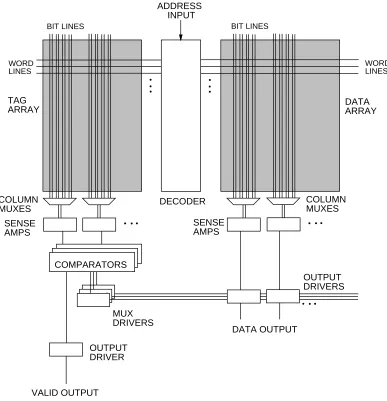
3. Cache Structure
Before describing the model, the internal structure of an SRAM cache will be briefly reviewed. Figure 1 shows the assumed organization. The decoder first decodes the address and selects the appropriate row by driving one wordline in the data array and one wordline in the tag array. Each array contains as many wordlines as there are rows in the array, but only one wordline in each array can go high at a time. Each memory cell along the selected row is as-sociated with a pair of bitlines; each bitline is initially precharged high. When a wordline goes high, each memory cell in that row pulls down one of its two bitlines; the value stored in the memory cell determines which bitline goes low.
Each sense amplifier monitors a pair of bitlines and detects when one changes. By detecting which line goes low, the sense amplifier can determine what is in the memory cell. It is possible for one sense amplifier to be shared among several pairs of bitlines. In this case, a multiplexor is inserted before the sense amps; the select lines of the multiplexor are driven by the decoder. The number of bitlines that share a sense amplifier depends on the layout parameters described in the next section. Section 6.4 discusses this further.
The information read from the tag array is compared to the tag bits of the address. In an A-way set-associative cache, A comparators are required. The results of the A comparisons are used to drive a valid (hit/miss) output as well as to drive the output multiplexors. These output multiplexors select the proper data from the data array (in a set-associative cache or a cache in which the data array width is larger than the output width), and drive the selected data out of the cache.
DATA ARRAY TAG
ARRAY
DECODER
COMPARATORS
COLUMN MUXES
OUTPUT DRIVERS SENSE
AMPS SENSE
AMPS COLUMN MUXES
MUX DRIVERS
ADDRESS INPUT
BIT LINES
WORD LINES BIT LINES
WORD LINES
VALID OUTPUT
DATA OUTPUT
[image:13.612.130.517.75.476.2]OUTPUT DRIVER
Figure 1: Cache structure
longer to read the data array, then the data side is the critical path. Since either side could deter-mine the access time, both must be modeled in detail.
4. Cache and Array Organization Parameters
The following cache parameters are used as inputs to the model: •C: Cache size in bytes
•B: Block size in bytes •A: Associativity
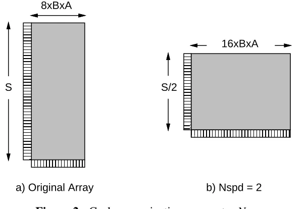
In addition, there are six array organization parameters. In the basic organization discussed by Wada [8], a single set shares a common wordline. Figure 2-a shows this organization, where B is the block size (in bytes), A is the associativity, and S is the number of sets (S = ). C Clearly,
B×A
such an organization could result in an array that is much larger in one direction than the other, causing either the bitlines or wordlines to be very slow. This could result in a longer-than-necessary access time. To alleviate this problem, Wada describes how the array can be broken horizontally and vertically and defines two parameters, Ndwl and Ndbl which indicates to what extent the array has been divided. The parameter Ndwl indicates how many times the array has been split with vertical cut lines (creating more, but shorter, wordlines), while Ndblindicates how many times the array has been split with horizontal cut lines (causing shorter bitlines). The total number of subarrays is Ndwl×Ndbl.
Figure 2-b introduces another organization parameter, Nspd. This parameter indicates how many sets are mapped to a single wordline, and allows the overall access time of the array to be changed without breaking it into smaller subarrays.
8xBxA
S S/2
16xBxA
[image:14.612.142.445.294.501.2]b) Nspd = 2 a) Original Array
Figure 2: Cache organization parameter Nspd
The optimum values of Ndwl, Ndbl, and Nspd depend on the cache and block sizes, as well as the associativity.
Notice that increasing these parameters is not free in terms of area. Increasing Ndbl or Nspd beyond one increases the number of sense amplifiers required, while increasing Ndwl means more wordline drivers are required. Except in the case of a direct-mapped cache with the block length equal to the processor word length and all three parameters equal to one, a multiplexor is required to select the appropriate sense amplifier output to return to the processor. Increasing Ndblor Nspdincreases the size of the multiplexor.
Using these organizational parameters, each subarray contains 8×B×A×Nspd columns and
Ndwl
rows.
We assume that the tag array can be broken up independently of the data array. Thus, there are also three tag array parameters: Ntwl, Ntbl, and Ntspd.
5. Methodology
The analytical model in this paper was obtained by decomposing the circuit into many equiv-alent RC circuits, and using simple RC equations to estimate the delay of each stage. This sec-tion shows how resistances and capacitances were estimated, as well as how they were combined and the delay of a stage calculated.
5.1. Equivalent Resistances
The equivalent resistance seen between drain and source of a transistor depends on how the transistor is being used. For each type of transistor (p and n), we will need two resistances: full-on and switching.
5.1.1. Full-on Resistance
The full-on resistance is the resistance seen between drain and source of a transistor assuming the gate voltage is constant and the gate is fully conducting. This resistance can be used for pass-transistors that (as far as the critical path is concerned) are always conducting. Also, this is the resistance that is used in the Horowitz approximation discussed in Section 5.5.
It was assumed that the equivalent resistance of a conducting transistor is inversely propor-tional to the transistor width (only minimum-length transistors were considered). The equivalent resistance of any transistor can be estimated by:
resn,on( W ) = Rn,on
W (1)
resp,on( W ) = Rp,on
W
where Rn,onand Rp,on are technology dependent constants. Appendix II shows values for these two parameters in a 0.8µm CMOS process.
5.1.2. Switching Resistance
This is the effective resistance of a pull-up or pull-down transistor in a switching static gate. For the most part, our model uses an inverter approximation due to Horowitz (see Section 5.5) to model such gates, but a simpler method using the static resistance is used to estimate the wordline driver size and the precharge delay.
Again, we assume the equivalent resistance of a conducting transistor is inversely proportional to the transistor width. Thus,
resn,switching( W ) = Rn,switching
W (2)
resp,switching( W ) = Rp,switching
where Rn,switching and Rp,switching are technology dependent constants (see Appendix II). The values shown in Appendix II were measured using Hspice simulations with equal input and out-put transition times.
5.2. Gate Capacitances
The gate capacitance of a transistor consists of two parts: the capacitance of the gate, and the capacitance of the polysilicon line going into the gate. If Leffis the effective length of the tran-sistor, Lpolyis the length of the poly line going into the gate, Cgateis the capacitance of the gate per unit area, and Cpolywireis the poly line capacitance per unit area, then a transistor of width W has a gate capacitance of:
gatecap = W×Leff×Cgate + Lpoly×Leff×Cpolywire
The same formula holds for both NMOS and PMOS transistors.
The value of Cgatedepends on whether the transistor is being used as a pass transistor, or as a pull-up or pull-down transistor in a static gate. Thus, two equations for the gate capacitance are required:
gatecap ( W , Lpoly) = W×Leff×Cgate + Lpoly×Leff×Cpolywire (3)
gatecappass( W , Lpoly) = W×Leff×Cgate,pass + Lpoly×Leff×Cpolywire
Values for Cgate, Cgate,pass, Cpolywire, and Leffare shown in Appendix II. A different Lpolywas used in the model for each transistor. This Lpolywas chosen based on typical poly wire lengths for the structure in which it is used.
5.3. Drain Capacitances
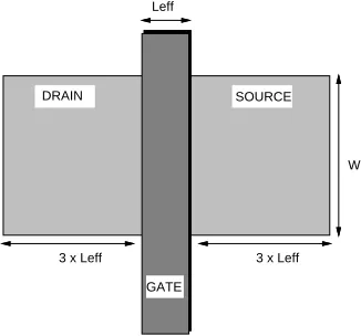
Figures 3 and 4 show typical transistor layouts for small and large transistors respectively. We have assumed that if the transistor width is larger than 10µm, the transistor is split as shown in Figure 4.
GATE Leff
W
3 x Leff 3 x Leff
[image:16.612.206.369.501.653.2]SOURCE DRAIN
Figure 3: Transistor geometry if width < 10µm
GATE
Leff
3 x Leff 3 x Leff
SOURCE DRAIN
3 x Leff SOURCE
W/2
Figure 4: Transistor geometry if width >= 10µm
draincap(W) = 3 Leff×W×Cdiffarea + ( 6 Leff+ W )×Cdiffside + W×Cdiffgate
where Cdiffarea, Cdiffside, and Cdiffgateare process dependent parameters (there are two values for each of these: one for NMOS and one for PMOS transistors). Cdiffgate includes the junction capacitance at the gate/diffusion edge as well as the oxide capacitance due to the gate/source or gate/drain overlap. Values for n-channel and p-channel Cdiffgateare also given in Appendix II.
If the width is larger than 10µm, we assume the transistor is folded (see Figure 4), reducing the drain capacitance to:
draincap(W) = 3 Leff× ×W Cdiffarea + 6 Leff ×Cdiffside + W×Cdiffgate
2
Now, consider two transistors (with widths less than 10µm) connected in series, with only a single Leff×W wide region acting as both the source of the first transistor and the drain of the second. If the first transistor is on, and the second transistor is off, the capacitance seen looking into the drain of the first is:
draincap(W) = 4 Leff×W×Cdiffarea + ( 8 Leff+ W )×Cdiffside + 3 W×Cdiffgate
Figure 5 shows the situation if the transistors are wider than 10µm. In this case, the capacitance seen looking into the drain of the inner transistor (x in the diagram) assuming it is on but the outer transistor is off is:
draincap(W) = 5 Leff× ×W Cdiffarea + 10 Leff×Cdiffside + 3 W×Cdiffgate
2
To summarize, the drain capacitance of x stacked transistors is:
if W < 10µm (4)
draincapn(W,x) =3 Leff×W×Cn,diffarea+ ( 6 Leff+ W )×Cn,diffside+ W×Cn,diffgate+ ( x−1 )×{Leff×W×Cn,diffarea+ 2 Leff×Cn,diffside+ 2 W×Cn,diffgate} draincapp(W,x) =3 Leff×W×Cp,diffarea+ ( 6 Leff+ W )×Cp,diffside+ W×Cp,diffgate+
x
3xLeff
Leff
3xLeff W/2
Leff
3xLeff
Figure 5: Two stacked transistors if each width >= 10µm
if W >= 10µm
draincapn(W,x) =3 Leff×W / 2×Cn,diffarea+ 6 Leff×Cn,diffside+ W×Cn,diffgate+ ( x−1 )×{Leff×W×Cn,diffarea+ 4 Leff×Cn,diffside+ 2 W×Cn,diffgate} draincapp(W,x) =3 Leff×W / 2×Cp,diffarea+ 6 Leff×Cp,diffside+ W×Cp,diffgate+
( x−1 )×{Leff×W×Cp,diffarea+ 4 Leff×Cp,diffside+ 2 W×Cp,diffgate}
5.4. Other Parasitic Capacitances
Other parasitic capacitances such as metal wiring are modeled using the values forbitmetaland Cwordmetal given in Appendix II. These capacitance values are fixed values per unit length in terms of the RAM cell length and width. These values include an expected value for the area and sidewall capacitances to the substrate and other layers. Besides being used for parasitic capacitance estimation of the bitlines and wordlines themselves, they are also used to model the capacitance of the predecode lines, data bus, address bus, and other signals in the memory. Al-though the capacitance per unit length would probably less for many of these busses than for the bit lines and word lines, the same value is used for simplicity of modeling.
5.5. Horowitz Approximation
In [2], Horowitz presents the following approximation for the delay of a static inverter with a rising input:
delayrise( tf, trise, vth) = tf √(log [ vth])2+ 2 triseb (1−vth) / tf
For a falling input with a fall time of tf, the above equation becomes:
delayfall( tf, tfall, vth) = tf √(log [ 1−vth])2+ 2 tfallb vth/ tf In this case, we used b=0.4.
The delay of an inverter is defined as the time between the input reaching the switching volt-age (also called threshold voltvolt-age) of the inverter and the output reaching the switching voltvolt-age of the following gate. If the inverter drives a gate with a different switching voltage, the above equations need to be modified slightly. If the switching voltage of the switching gate is vth1and the switching voltage of the following gate is vth2, then:
delayrise( tf, trise, vth1,vth2) = tf√(log [ vth1])2+ 2 triseb (1−vth1) / tf + (5)
tf ( log [vth1]−log [vth2] )
delayfall( tf, tfall, vth1,vth2) = tf √(log [ 1−vth1])2+ 2 tfallb vth1/ tf +
tf ( log [1−vth1]−log [1−vth2] )
6. Delay Model
This section derives the cache read access and cycle time model. From Figure 1, the follow-ing components can be identified:
•Decoder
•Wordlines (in both the data and tag arrays) •Bitlines (in both the data and tag arrays)
•Sense Amplifiers (in both the data and tag arrays) •Comparators
•Multiplexor Drivers
•Output Drivers (data output and valid signal output)
The delay of each these components will be estimated separately (Sections 6.1 to 6.10), and will then be combined to estimate the access and cycle time of the entire cache (Section 6.11).
6.1. Decoder
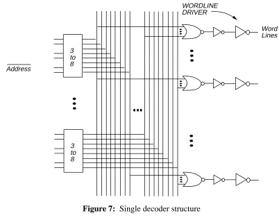
6.1.1. Decoder Architecture
Figures 6 and 7 show the decoder architecture. It is assumed that each subarray has its own decoder; therefore, there are Ndwl×Ndbl decoders associated with the data array, and Ntwl×Ntbl tag array decoders. One driver drives all the data array decoders, while another drives the tag array decoders.
ARRAY
DECODER
ARRAY
DECODER
ARRAY
DECODER
ARRAY
DECODER
ARRAY
DECODER
ARRAY
DECODER
ARRAY
DECODER
ARRAY
DECODER
ADDRESS
Ndwl*Ndbl Data Arrays
[image:20.612.162.413.69.287.2]Ntwl*Ntbl Tag Arrays
Figure 6: Decoders with decoder driver
3 to 8 3 to 8
WORDLINE DRIVER
Word Lines
Address
Figure 7: Single decoder structure
log2( )C
B A NdblNspd
bits that must be decoded, the number of 3-to-8 blocks required is simply:
N3to8 = 1log2( ) 3
C
[image:20.612.84.486.315.629.2](if the number of address bits is not divisible by three, then 1-of-4 codes can be used to make up the difference, but this was not modeled here).
These 1-of-8 codes are combined using NOR gates in the second stage. One NOR gate is required for each of the B×A×NC rows in the subarray. Each NOR gate must take one input
dbl×Nspd
from each 3-to-8 block; thus, each NOR gate has N3to8inputs (where N3to8was given in Equa-tion 6).
The final stage is an inverter that drives each wordline driver.
6.1.2. Decoder Delay
Figure 8 shows a transistor-level diagram of the decoder. The decoder delay is the time after the input passes the threshold voltage of the decoder driver until norout reaches the threshold voltage of the final inverter (before the wordline driver). Notice that the delay does not include the time for the inverter to drive the wordline driver; this delay depends on the size of the wordline driver and will be considered in Section 6.2.
Since, in many caches, decbus will be precharged before a cache access, the critical path will include the time to discharge decbus. This occurs after nandin rises, which in turn, is caused by address bits (or their inverses) falling. Once decbus has been discharged, norout will rise, and after another inverter and the wordline driver, the selected wordline will rise.
Only one path is shown in the diagram; the extra inputs to the NAND gates are connected to other outputs of the decoder driver, and the extra inputs to the NOR gates are connected to the outputs of other NAND gates. The worst case for both the NAND and NOR stages occurs when all inputs to the gate change. This is the case that will be considered when estimating the decoder delay.
6.1.3. Input Fall Time
The delay of the first stage depends on the fall time of the input. To estimate a reasonable value for the input fall time, two inverters in series as shown in Figure 9 are considered. Each inverter is assumed to be the same size as the decoder driver (the first inverter in Figure 8).
The Horowitz inverter approximation of Equation 5 is used to estimate the delay of each in-verter (and hence the output rise time). The time constant, tf, of the first stage is Req×Ceqwhere Req is the equivalent resistance of the pull-up transistor in the inverter (the full-on resistance, as described in Section 5.1) and Ceq is the drain capacitance of the two transistors in the first in-verter stage plus the gate capacitance of the two transistors in the second stage (Sections 5.3 and 5.2 show how these can be calculated). The input fall time of the first stage is assumed to be 0 (a step input), and the initial and final threshold voltages are the same. Thus, the delay of the first inverter can be written using the notation in Section 5 as:
T1 = delayfall( tf, 0 , vthdecdrive, vthdecdrive)
where
tf = resp,on( Wdecdrivep)×
( draincapn( Wdecdriven, 1 ) + draincapp( Wdecdrivep, 1 ) +
ROWS
8 NOR GATES
To
Ndwl*Ndbl−1 other decoders in
nandin
decbus
norout
Wordline Driver
Figure 8: Decoder critical path
in step
input x
Figure 9: Circuit used to estimate reasonable input fall time
In the above equation, the widths of the transistors in the inverter transistors are denoted by Wdecdriven and Wdecdrivep and the threshold (switching) voltage of the inverter is denoted by vthdecdrive. Appendix I shows the assumed sizes and threshold voltages for each gate on the critical path of the cache.
From the above equation, the rise time to the second stage can be approximated as T1 .
The second stage can be worked out similarly:
T2 = delayrise( tf, , vT1 thdecdrive, vthdecdrive)
vthdecdrive
From this, the fall time of the second inverter output (and hence a reasonable fall time for the cache input) can be written as:
infalltime =
T2
1−vthdecdrive (7)
Note that the above expressions for T1and T2will not be included in the cache access time; they were only derived to estimate a reasonable input fall time (Equation 7).
6.1.4. Stage 1: Decoder Driver
This section estimates the time for the first inverter in Figure 8 to drive the NAND inputs. Each inverter drives 4×Ndwl×Ndbl NAND gates (recall that both address and address-bar are as-sumed to be available; thus, each driver only needs to drive half of the NAND gates in its 3-to-8 block).
Vdd
eq
R
Ceq nandin
Figure 10: Decoder driver equivalent circuit
Figure 10 shows a simplified equivalent circuit. In this figure, Req is the equivalent pull-up resistance of the driver transistor plus the resistance of the metal lines used to tie the NAND outputs to the NOR inputs. The wire length can be approximated by noting that the total edge length of the memory is approximately 8×B×A×Ndbl×Nspd cells. If the memory arrays are grouped in two-by-two blocks, and if the predecode NAND gates are at the center of each group, then the connection between the driver and the NAND gate is one quarter of the sum of the array widths (see Figure 11). In large memories with many groups the bits in the memory are arranged so that all bits driving the same data output bus are in the same group, reducing the required length of the data bus.
Thus, if Rwordmetalis the approximate resistance of a metal line per bit width, then Reqis:
Req = resp,on( Wdecdrivep) + Rwordmetal× 8 B A NdblNspd 8
Pre-decode Address in
from driver
Predecoded address
Channel for data output bus
Figure 11: Memory block tiling assumptions
The equivalent capacitance Ceqin Figure 10 can be written as:
Ceq = draincapp( Wdecdrivep, 1 ) + draincapn( Wdecdriven,1 ) +
4 NdwlNdblgatecap ( Wdec3to8n+ Wdec3to8p, 10 ) + 2 B A NdblNspdCwordmetal
where Cwordmetalis the metal capacitance of a metal wire per bit width.
Using Reqand Ceq, the delay can be estimated as:
(8)
Tdec,1 = delayfall( CeqReq, infalltime , vthdecdrive, vthdec3to8)
where infalltime is from Equation 7.
6.1.5. Stage 2: NAND Gates
This section estimates the time required for a NAND gate to discharge the decoder bus (and the inputs to the NOR gates). The equivalent circuit is shown in Figure 12. In this diagram, Req
eq
C R
eq
decbus
Figure 12: Decoder driver equivalent circuit
approximated by 3 resn,on(Wdec3to8n). Since all three inputs are changing simultaneously (in the worst case), each transistor has about the same resistance. In our CMOS 0.8µm process, this approximation induces an error of about 10%-20%. The resistance Req also includes the metal
resistance of the lines connecting the NAND to the NOR gate. Since there are B A NC rows in
dblNspd
the subarray,
Req = 3 resn,on(Wdec3to8n) + Rbitmetal× C 2 B A NdblNspd
where Rbitmetalis the metal resistance per bit height.
The capacitance Ceq is the sum of the input capacitances of 8 B A NC NOR gates, the drain
dblNspd
capacitances of the NAND driver, and the wire capacitance. Thus,
Ceq = 3 draincapp( Wdec3to8p, 1 ) + draincapn( Wdec3to8n, 3 ) +
×gatecap(Wdecnorn+Wdecnorp,10 ) + ×Cbitmetal C
8 B A NdblNspd
C
2 B A NdblNspd
The delay of this stage is given by:
Tdec,2 = delayrise( Req×Ceq, , vTdec,1 thdec3to8, vthdecnor)
vthdec3to8 (9)
where Tdec,1is from Equation 8.
6.1.6. Stage 3: NOR Gates
The final part of the decoder delay is the time for a NOR gate to drive norout high. An equivalent circuit similar to that of Figure 10 can be used. In this case, the pull-up resistance of the NOR gate is approximated by N3to8×resp(Wdecnorp) where N3to8 is the number of inputs to each NOR gate (from Equation 6). The capacitance Ceqis
Ceq = N3to8draincapn( Wdecnorn, 1 ) + draincapp( Wdecnorp, N3to8) +
gatecap ( Wdecinvn+ Wdecinvp)
Then,
Tdec,3 = delayfall( Req×Ceq, , vthdecnor, vthdecinv)
Tdec,2
1−vthdecnor (10)
where Tdec,2 is from Equation 9. Note that the value of vthdecnor depends on the number of inputs to each NOR gate (Appendix I contains several values for vthdecnor).
6.1.7. Total decoder delay
By adding equations 8 to 10, the total decoder delay can be obtained:
6.1.8. Analytical vs. Hspice Results
Figure 13 shows the decoder delay predicted by Equation 11 (solid lines) as well as the delay predicted by Hspice (dotted lines). The transistor sizes used in the Hspice model are shown in Appendix I and the technology parameters used are shown in Appendix II. The Hspice deck used in this (and all other graphs in this paper) models an entire cache; this ensures that the input slope and output loading effects of each stage are properly modeled.
The horizontal axis of Figure 13 is the number of rows in each subarray (which is B A NC ).
dblNspd
The results are shown for one and eight subarrays. The analytical and Hspice results are in good agreement. The step in both results is due to a change from 3-input to 4-input NOR gates in the final decode when moving from 9 address bits to 10 address bits.
Decoder Delay
Rows in Each Array 0ns
1ns 2ns 3ns 4ns 5ns 6ns 7ns 8ns
0 200 400 600 800
. . . .
g g
Analytical Hspice
1 Array 8 Arrays
g g g g
g g g g
g g g g g g
g g g g
g g g
g
g g g g
g g g g
g g g g g g
g g g g
g g g
g
Figure 13: Decoder delay
6.1.9. Tag array decoder
6.2. Wordlines
6.2.1. Wordline Architecture
Figure 14 shows the wordline driver driving a wordline. The two inverters are the same as the final two inverters in Figure 8 (recall that the decoder equations do not include the time to dis-charge the decoder output).
8 x B x A x Nspd Ndwl Bits
norout
decout word
Wordline Driver
Figure 14: Word line architecture
In Wada’s access time model, it was assumed that wordline drivers are always the same size, no matter how many columns are in the array. In this model, however, the wordline driver is assumed to get larger as the wordline gets longer. Normally, a cache designer would choose a target rise time, and adjust the driver size appropriately. Rather than assuming a constant rise time for caches of all sizes, however, we assume the desired rise time (to a 50% word line swing) is:
rise time = krise×ln ( cols )×0.5 where
cols = 8 B A Nspd
Ndwl
The constant kriseis a constant that depends on the implementation technology. To obtain the transistor size that would give this rise time, it is necessary to work backwards, using an equiv-alent RC circuit to find the required driver resistance, and then finding the transistor width that would give this resistance.
Vdd
R
Ceq word
p
Figure 15 shows the equivalent circuit for the wordline. The pull-up resistance can be ob-tained using the following RC equation
Rp = − rise time
Ceq×ln ( vthwordline) (12)
where Vthwordline is inverter threshold (relative to Vdd). This is significantly higher than the voltage (Vt) at which the pass transistors in the memory cells begin to conduct. The use of the inverter threshold gives a more intuitive delay for the wordline but it can result in negative bit-line delays.
The line capacitance is approximately the sum of gate capacitances of each memory cell in the row (a more detailed equation will be given later):
Ceq = cols ×( 2×gatecappass(Wa, 0 ) + Cwordmetal)
This equation was derived by noting the wordline drives the gates of two pass transistors in each bit (the memory cell is shown in Figure 19).
Once Rpis found using Equation 12, the pull-up transistor’s width can be found using:
Wdatawordp = Rp,switching
Rp
where Rp,switching is a constant that was discussed in Section 5.1.2. When calculating capacitances, we will assume that the width of the NMOS transistor in the driver is half of Wdatawordp.
6.2.2. Wordline Delay
There are two components to the word-line delay: the time to discharge the input of the wordline driver, and the time for the wordline driver to charge the wordline.
Consider the first component. The capacitance that must be discharged is:
Ceq= draincapn(Wdecinvn, 1 ) + draincapp(Wdecinvp, 1 ) +
gatecap( Wdatawordp+ 0.5 Wdatawordp, 20 )
The equivalent resistance of the pull-down transistor is simply
Req = resn,on( Wdecinvn)
The delay is then
Tword,1 = delayrise( Req×Ceq, , vTdec,3 thdecinv, vthworddrive)
vthdecinv (13)
where Tdec,3 is the delay of the final decoder stage (from Equation 10). Note that in general, vthworddrivewill depend on the size of the wordline driver. If a constant ratio between the widths of the NMOS and PMOS driver transistors is used, however, the threshold voltage is almost constant.
From the previous section, the delay of the second stage is approximately
Tword,2,approx = krise×ln ( cols )×vthwordline
Req = resp,on(Wdatawordp) + cols×Rwordmetal 2
Ceq= 2 cols×gatecappass(Wa, BitWidth−2 Wa) +
draincapp( Wdatawordp, 1 ) + draincapn( 0.5 Wdatawordp, 1 ) + cols ×Cwordmetal
The quantity BitWidth in the above equation is the width (inµm) of one memory cell. Using Ceqand Req, the time to charge the wordline is:
Tword,2 = delayfall( Req×Ceq, , vTword,1 thworddrive, vthwordline)
1−vthworddrive (14)
Equations 13 and 14 can then be combined to give the total wordline delay:
Twordline,data = Tword,1+ Tword,2 (15)
6.2.3. Analytical and Hspice Comparisons
As before, the analytical model was compared to results obtained from Hspice simulations. The technology parameters and transistor sizes shown in Appendices I and II were used, and the results in Figure 16 were obtained. The wordline in the Hspice deck was split into 8 sections, each section containing one eighth of the memory cells. The sections were separated by one eighth of the wordline resistance. As the graph shows, the equation matches the Hspice measurements very closely.
Wordline Delay (data array)
Columns in Each Array 0ns
0.5ns 1.0ns 1.5ns 2.0ns
100 200 300 400 500 600
. . . .g g
Analytical
HSpice g
.. .g . ... .g
.g . ..g. .
. g . . .. .g . .
. ... . .g . . ..g. . .
. . ... . .g
. . . .g. . . .. . .g
. . . .. . .g. . . .
. . .. . . .g . . .g
6.3. Tag Wordline
Unlike the driver for the data array wordlines, it was assumed that the size of the wordline driver in the tag array is constant for all cache sizes since the tag array is (usually) much nar-rower than the data array.
Figure 14 can be used to estimate the delay of the tag wordline. Again, there are two com-ponents to the delay: the time to discharge the wordline driver, and the time to charge the wordline itself. For the first component, the previous equations can be used:
Ceq=draincapn(Wdecinvn, 1 ) + draincapp(Wdecinvp, 1 ) + gatecap( Wtagwordp+ Wtagwordn, 20 )
Req=resn,on( Wdecinvn)
Ttagword,1 = delayrise( Req×Ceq, , vTdec,3 thdecinv, vthtagworddrive)
vthdecinv
where Tdec,3is the delay of the final decoder stage (from Equation 10). Note that in these equa-tions, Wtagwordpand Wtagwordnare constants (unlike the equations in the previous section).
The second component is slightly different. If an address contains baddr bits, then the number of bits in a tag is:
tagbits = baddr− log2( cache size in bytes ) + log2( associativity ) + 2 (16) The "+2" is because of the valid and dirty bits. This quantity can then be used in:
Req = resp,on(Wtagwordp) + tagbits×Rwordmetal 2
Ceq = 2 tagbits ×gatecappass( Wa, BitWidth−2×Wa) +
draincapp( Wtagwordp, 1 ) + draincapn( Wtagwordn, 1 ) + tagbits ×Cwordmetal
to give
Ttagword,2 = delayfall( Req×Ceq, , vTtagword,1 thtagworddrive, vthwordline)
1−vthtagworddrive (17)
The equations for Ttagword,1 and Ttagword,2 can then be summed to give the total delay at-tributed to the tag array wordline:
Twordline,tag = Ttagword,1+ Ttagword,2 (18)
Wordline Delay (tag array)
Address Bits (C=8192, A=1) 0ns
0.5ns 1.0ns
16 32 48 64
. . . .
g g
Analytical HSpice g
. . .. . . . . .. . .
. . .. . . . .g. . .. . .
. . .. . . . . .. . .
. .g. . .. . . . . .. . .
[image:31.612.177.527.84.345.2]. . .. . . . .g
Figure 17: Wordline of tag array
6.4. Bit Lines
6.4.1. Bitline architecture
Each column in the array has two bitlines: bit and bitbar. After one of the wordlines goes high, each memory cell in the selected row begins to pull down one of its two bitlines; which bitline drops depends on the value stored in that memory cell.
In most memories, the bitlines are initially precharged high and equilibrated using a circuit like the one shown in Figure 18. During the precharge phase, both bitlines are charged to the same voltage, Vbitpre. The four NMOS transistors in the figure are connected as diodes; their only purpose is to drop the precharged voltage from Vddto Vbitpre(in our process, Vddis 5 volts and Vbitpreis 3.3 volts). The sense amplifier that will be described in the next section requires that the common mode voltage on the bitlines be less than Vdd.
A typical SRAM cell is shown in Figure 19. When the wordline goes high, the Watransistors will begin to conduct, discharging one of the bitlines.
Bit Bitbar Precharge
V
dd Vdd
Figure 18: Precharging and equilibration transistors
Bit Bitbar
Word
W
a Wa
W b
W d
W
bW d
Figure 19: One memory cell
Sense Amp BITLINES
TO PRECHARGE CIRCUIT
6.4.2. Bitline delay
The delay of the bitline is defined as the time between the wordline going high (reaching Vthwordline) and one of the bitlines going low (reaching a voltage of Vbitsensebelow its maximum value).
6.4.3. Equivalent Circuit
As previously mentioned, in each row, either bit or bitbar will go low. Consider the case when bit goes low. The equivalent circuit in Figure 21 can be used. The transistors labeled Wa
C colmux
C
line Rmem
R line
R colmux
Figure 21: Bitline equivalent circuit
and Wd have been replaced by a resistor with resistance Rmem. The capacitance Cline includes the capacitance of the memory cells sharing the bitline, the metal line capacitance, the drain capacitance of the precharge circuit, and the drain capacitance of the column multiplexor pass transistor:
Cline = ( rows )×(1draincapn(Wa, 1 ) + Cbitmetal) +
2 (19)
2 draincapp( Wbitpreequ, 1 ) + draincapn(Wbitmuxn, 1 )
where
rows = C
B A NdblNspd (20)
The drain capacitance of each Wa transistor is divided by two since each contact is shared be-tween two vertically adjacent cells.
The capacitance Ccolmux in Figure 21 is the capacitance seen by the output of the conducting column multiplexor pass transistor. It includes the drain capacitance of all pass transistors con-nected to this sense amplifier and the input capacitance of the sense amplifier:
Ccolmux = ( NspdNdwl)×draincapn( Wbitmuxn, 1 ) + (21)
2 gatecap ( WsenseQ1to4, 10 )
The resistance Rcolmuxis simply:
Rcolmux = resn,on( Wbitmuxn) (22)
Cline = ( rows )×[1draincapn(Wa, 1 ) + Cbitmetal] + 2 draincapp( Wbitpreequ, 1 )
2 (23)
Ccolmux = 2 gatecap ( WsenseQ1to4, 10 )
Rcolmux = 0
The resistances Rmem and Rlinedo not depend on the value of Ndbl×Nspd. Rmem is the equiv-alent resistance of the conducting transistors in the memory cell:
Rmem = resn,on( Wa, 1 ) + resn,on( Wd, 1 ) (24)
Finally, Rlineis the metal resistance of the bitline. As before, we assume that the resistance is clumped rather than distributed over the entire line. Thus,
Rline = rows Rbitmetal
2 (25)
where the number of rows is as in Equation 20.
6.4.4. Equivalent circuit solution
Figure 21 can be viewed as an RC tree as described in [7]. Using the simple single time constant approximation, the delay can be written as:
Tstep= [ RmemCline+ ( Rmem+ Rline+ Rcolmux) Ccolmux] ln ( Vbitpre )
Vbitpre−Vbitsense (26)
6.4.5. Non-zero wordline rise times
Equation 26 assumes that there is a step input on the wordline. This subsection describes how the non-zero wordline rise time can be taken into account.
Figure 22 shows the wordline voltage (the input to the bitline circuit) as a function of time assuming a step input on the wordline. The time difference Tstepshown on the graph is the time after the wordline rises until the bitline reaches Vbitpre−Vbitsense (the bitline voltage is not shown on the graph). Tstep is given by Equation 26. During this time, we can consider the bitline being "driven" towards Vbitpre−Vbitsense. Because the current sourced by the access tran-sistor i can be approximated as
i ≈ gm( Vgs − Vt)
the shaded area in the graph can be thought of as the amount of charge discharged before the output reaches Vbitpre−Vbitsense. This area can be calculated as:
area = Tstep × (Vdd−Vt)
(Vtis the voltage at which the NMOS pass transistor begins to conduct).
t word line
voltage
T step t
v Vdd
Figure 22: Step input on wordline
Tbitline,data = −2 ( vs−vt) +√4 ( vs−vt)
2−4×m×c
2×m (27)
where
c = ( v1 s−vt)2 − 2 Tstep( Vdd−vt)
m
and m is the slope of the input waveform.
t word line
voltage
slope = m
v s
v t vdd
Tbit,data area = T
step(Vdd−vt)
Figure 23: Slow-rising wordline
If the wordline rises quickly, as shown in Figure 24, then the algebra is slightly different. In this case,
Tbitline,data = Tstep + Vdd+ Vt − 2 m
vs
m (28)
The cross-over point between the two cases for Tbitlineoccurs when:
Tstep = Vdd−Vt 2 m
t word line
voltage
slope = m
area = T
step(Vdd−v t )
Tbit,data v
t V
dd
v s
Figure 24: Fast-rising wordline
m = Vdd−Vt
2 Tstep
Calculating the slope, m, for a given wordline rise time is simple. From section 6.2: rise time = krise×ln ( cols )
Thus,
m = Vdd
krise×ln ( cols )
For most practical cases, the input rise time is slow enough that Equation 27 should be used. However, it is always important to check the size of m before calculating Tbitline,data.
6.4.6. Analytical vs. Hspice Results
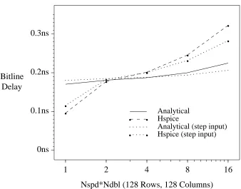
Again, an Hspice model was used to validate the analytical equations. Figure 25 shows the bitline delay for an array with 128 columns and no column-multiplexing. The lower two lines show the analytical and Hspice results assuming a step input on the wordline. The upper lines show the results if a non-zero wordline rise time is assumed. As the graph shows, for a wide range of array sizes (number of rows) the analytical predictions closely match the Hspice results. (The bitlines appear to have a negative delay for very small numbers of rows due to the relative thresholds used for the wordline and bitline delays.)
Figure 26 shows the same thing if 8-way column multiplexing is used; that is, a single sense amplifier is shared among 8 pairs of bitlines. The error is somewhat larger than in Figure 25, but the analytical and Hspice results are still within 0.1ns of each other.
Bitline Delay
Rows (128 Columns, Nspd*Ndbl=1) 0ns 0.1ns 0.2ns 0.3ns 0.4ns 0.5ns 0.6ns 0.7ns 0.8ns
100 200 300 400 500
. . . . . . . . g g g g Analytical Hspice
Analytical (step input) Hspice (step input)
. .. . .. .. . .. .. . .. .. . .. .. . .. .. . .. .. . .. .. . .. .. . .. .. . .. .. . .. .. . .. .. . . g g g g g g g g g g g g g g g . . .. .g. . .
. .g. . .. .g . . .. .g. . .
. .g. . .. .g. . . . .. . .g . .g
. . .. .g. . . . .. . .g . .g
. . .. .g. . . . .g
Figure 25: Bitline results without column multiplexing
Bitline Delay
Rows (128 Columns, Nspd*Ndbl=8) 0ns 0.1ns 0.2ns 0.3ns 0.4ns 0.5ns 0.6ns 0.7ns 0.8ns
100 200 300 400 500
. . . . . . . . g g g g Analytical Hspice
Analytical (step input) Hspice (step input)
. .. . .. .. . .. .. . .. .. . .. .. . .. .. . .. .. . .. .. . .. .. . .. .. . .. .. . .. .. . .. .. . . g g g g g g g g g g g g g g g . . .. .g. . .
. .g. . .. .g . . .. .g. . .
. .g. . .. .g . . .. .. . .g
. .. . .g . .g . . .. .. . .g
. .. . .g . .g . . .. .g
Bitline Delay
Columns (128 Rows, Nspd*Ndbl=1) 0ns
0.05ns 0.1ns 0.15ns 0.2ns 0.25ns
100 200 300 400 500
. . . . . . . . g g
g g
Analytical Hspice
Analytical (step input) Hspice (step input)
. . . . .. . . . .. . . . .. . . . .. . . . .. . . . .. . . . .. . . . .. . . . .. . . . .. . . . .. . . . .. . . . .
g g
g g
g g
g g g
g g
g g g g
[image:38.612.139.478.73.335.2]. . . . .. . . . .g g. . . . .g. . . . .g. . . . .g. . . . .g. . . . .. . . . .g . . . . .g g. . . . .. . . . .g . . . . .g g. . . . .g
Figure 27: Bitline results vs. number of columns
Finally, Figure 28 shows how the delay is affected by the degree of column multiplexing. As expected, the larger the degree of multiplexing, the higher the delay, since more capacitance must be discharged when the bitline drops. Again, there is good agreement between the Hspice and analytical results.
6.4.7. Tag array bitlines
The equations derived in this section can be used for the tag array bitlines as well. The only difference (besides replacing the data array organizational parameters with the corresponding tag array parameters) is the calculation of the input rise time. The wordline rise time can be ap-proximated by:
rise time = Ttagword,2
vthwordline
where Ttagword,2was given in Equation 17. This leads to:
m = Vddvthwordline Ttagword,2
Bitline Delay
Nspd*Ndbl (128 Rows, 128 Columns) 0ns
0.1ns 0.2ns 0.3ns
1 2 4 8 16
. . . . . . . .
g g
g g
Analytical Hspice
Analytical (step input) Hspice (step input)
. . . .. . . .. . . .. . . ..
. . . .. . . . .
g
g
g
g
g
g . .. .
. .. . . .. .
. .. . . g
. . . .. . . .
. .g. . . .. . . .
. . . .. . .g. . . . . .. . .
[image:39.612.174.512.108.373.2]. . .. . . . g
Figure 28: Bitline results vs. degree of column multiplexing
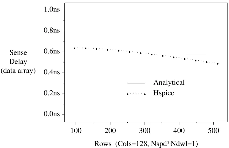
6.5. Sense Amplifier
Wada’s sense amplifier (reproduced in Figure 29) amplifies a voltage difference of 2×Vbitsense to Vdd. In [8], an approximation of the delay of the sense amplifier is written in terms of various process parameters. In this model, we encapsulate several of these parameters into a single process parameter, tsense,data, which is the delay of the sense amp:
Tsense,data = tsense,data (29)
The value of tsense,datacan be estimated from Hspice simulations. Figure 30 shows the delay measured from Hspice and the constant delay predicted by the model as a function of input fall-time (neither the analytical model used here nor Wada’s model took into account the effects of a non-zero bitline fall time). As the graph shows, the error is small.
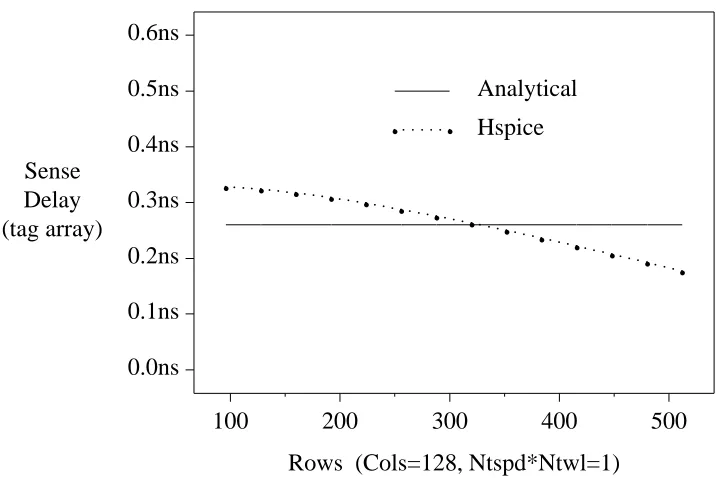
The delay of the sense amplifier in the tag array can also be approximated by a constant:
Tsense,tag = tsense,tag (30)
V dd
Q 1 Q2 Q
7 Q 8
Q 13
V dd
Q Q
Q Q
3 4
9 10
Q 14
V dd
Q Q
Q Q
5 6
11 12
Q15 V
dd
BIT BITBAR
[image:40.612.131.449.76.415.2]Out
Figure 29: Sense amplifier (from [8])
Sense Delay (data array)
Rows (Cols=128, Nspd*Ndwl=1) 0.0ns
0.2ns 0.4ns 0.6ns 0.8ns 1.0ns
100 200 300 400 500
. . . .
g g
Analytical Hspice
g
. . . . .g. . . . .g. . . . .g. . . . .g. . . . . g
. . . . .g. . . . . g
. . . . .g. . . . . g
. . . . .g. . . . . g
[image:40.612.140.505.449.686.2]. . . . .g. . . . . g
Sense Delay (tag array)
Rows (Cols=128, Ntspd*Ntwl=1) 0.0ns
0.1ns 0.2ns 0.3ns 0.4ns 0.5ns 0.6ns
100 200 300 400 500
. . . .
g g
Analytical
Hspice
g
. . . . .g. . . . . g
. . . . .g. . . . . g
. . . . .g. . . . . g
. . . . .g. . . . . g
. . . . .. . . . .g g
[image:41.612.176.537.66.305.2]. . . . .g. . . . . g . . . . .g
Figure 31: Tag array sense amplifier delay
The following stages will also require an approximation of the fall time of the sense amplifier output. A constant fall time for each sense amp was assumed. The fall times will be denoted by tfallsense,dataand tfallsense,tag; the values for our process are shown in Appendix I.
6.6. Comparator
6.6.1. Comparator Architecture
The comparator that was modeled is shown in Figure 32. The outputs from the sense amplifiers are connected to the inputs labeled bnand bn-bar. The anand an-bar inputs are driven by tag bits in the address. Initially, the output of the comparator is precharged high; a mismatch in any bit will close one pull-down path and discharge the output. In order to ensure that the output is not discharged before the bnbits become stable, node EVAL is held high until roughly three inverter delays after the generation of the bn-bar signals. This is accomplished by using a timing chain driven by a sense amp on a dummy row in the tag array. The output of the timing chain is used as a "virtual ground" for the pull-down paths of the comparator. When the large NMOS transistor in the final inverter in the timing chain begins to conduct, the virtual ground (and hence the comparator output if there is a mismatch) begins to discharge.
6.6.2. Comparator Delay
Since we assume that the anand bnbits will be stable by the time EVAL goes low, the critical path of the comparator is the propagation delay of the timing chain plus the time to discharge the output through the NMOS transistor in the final inverter.
a0
0 b a0
0
b b
a
b
a
b a
b 1
1 1
a
1 n
n
n
n Vdd
PRECHARGE
OUT
large n small p From
dummy row sense amp in tag array
[image:42.612.77.483.68.535.2]EVAL
Figure 32: Comparator
tf,1 = resp,on( Wcompinvp1)×[ gatecap( Wcompinvn2+ Wcompinvp2, 10) +
draincapp( Wcompinvp1, 1 ) + draincapn( Wcompinvn1, 1 ) ]
tf,2 = resn,on( Wcompinvn2)×[ gatecap( Wcompinvn3+ Wcompinvp3, 10) +
draincapp( Wcompinvp2, 1 ) + draincapn( Wcompinvn2, 1 ) ]
tf,3 = resp,on( Wcompinvp3)×[ gatecap( Wevalinvn+ Wevalinvp, 10) +
draincapp( Wcompinvp3, 1 ) + draincapn( Wcompinvn3, 1 ) ]
Tcomp,1 = delayfall( tf,1, tfallsense,tag, vthcompinv1, vthcompinv2)
Tcomp,2 = delayrise( tf,2, , vtf,1 thcompinv2, vthcompinv3)
vthcompinv2
Tcomp,3 = delayfall( tf,3, , vtf,2 thcompinv3, vthevalinv) 1−vthcompinv3
The final stage involves discharging the output through a pull-down path and the NMOS tran-sistor of the final inverter driver. An equivalent circuit is shown in Figure 33. The resistance Revalnis the resistance of the pull-down transistor in the final inverter:
Revaln = resn,switching( Wevalinvn)
In the worst case, only one pull-down path is conducting; the resistance Rpulldown is the path’s equivalent resistance. Since it was assumed that the inputs are stable when the evaluation takes place, we are interested in the full-on resistance of the pull-down path:
Rpulldown = 2 resn,on( Wcompn)
Revaln
Ceqtop C
eqbot
R
pulldown
out
Figure 33: Comparator equivalent circuit
Ceqbot = tabits ×[ draincapn(Wcompn,1) + draincapn(Wcompn,2) ] +
draincapp( Wevalinvp, 1 ) + draincapn( Wevalinvn, 1 )
where tagbits is the number of tag bits (from Equation 16). Note that there are 2×tagbits pull-down paths (two for each bit); half of the "off" paths have the top transistor off, and half have the bottom transistor off. We have also included the drain capacitances of the final inverter stage.
The capacitance Ceqtopcan be written similarly:
Ceqtop= tabits ×(draincapn(Wcompn,1) + draincapn(Wcompn,2)) + draincapp( Wcompp, 1 ) +
gatecap ( Wmuxdrv1n+ Wmuxdrv1p, 20 ) + tagbits ×NtblNtspdCwordmetal
The output capacitance is taken to be the input capacitance of either the multiplexor driver described in Section 6.7 or the valid signal driver in Section 6.9 (the first stage of both structures are the same, so they have the same input capacitance). We have also included metal capacitance of the metal output (it is assumed that the metal crosses the entire width of the tag array).
The circuit in Figure 33 is equivalent to the circuit in Figure 21, so the same solution can be used. The result is:
(31)
Tstep= [ RevalnCeqbot+ ( Revaln+ Rpulldown) Ceqtop] ln ( 1 )
vthmuxdrv1
The non-zero input fall time can be taken into account using the same method as Section 6.4. There are two possible equations; which one should be used depends on the slope of the input. For a slow rising input:
Teval = −2 ( vs−vt) +√4 ( vs−vt)
2−4×m×c
2×m (32)
where
c = ( v1 s−vt)2 − 2 Tstep( Vdd−Vt)
m
and m is the slope of the input waveform:
m = Tcomp,3 vthevalinv
m < Vdd−Vt
2 Tstep
For a quickly rising input (m greater than Vdd−Vt):
2 Tstep
Teval = Tstep + Vdd+ Vt − 2 m
vs
m (33)
The above equations can be combined to give the total delay due to the comparator:
Tcompare = Tcomp1+ Tcomp2+ Tcomp3+ Teval (34)
[image:44.612.132.477.269.504.2]6.6.3. Hspice Comparisons
Figure 34 compares the analytical model to a Hspice model of the circuit. As can be seen, there is good agreement between the two models.
Compare Delay
Tag Bits 0ns
1ns 2ns 3ns 4ns
0 10 20 30 40
. . . .
g g
Analytical Hspice g
. . ..g. . . . . ... . .g
. . ..g. . . . . ..g. . .
. . ..g. . . . . ..g. . .
. . ..g. . . . . ..g. . .
. . ..g. . . . . ..g
Figure 34: Comparator delay
6.7. Multiplexor Driver