X-ray spectroscopic study of the electronic structure of CuCrO
2T. Arnold, D. J. Payne, A. Bourlange, J. P. Hu, and R. G. Egdell*
Department of Chemistry, Inorganic Chemistry Laboratory, South Parks Road, Oxford OX1 3QR, United Kingdom
L. F. J. Piper, L. Colakerol, A. De Masi, P.-A. Glans, T. Learmonth, and K. E. Smith Department of Physics, Boston University, 590 Commonwealth Avenue, Boston, Massachusetts 02215, USA
J. Guo
Advanced Light Source, Lawrence Berkeley National Laboratory, Berkeley, California 94720, USA
D. O. Scanlon, A. Walsh,† B. J. Morgan, and G. W. Watson School of Chemistry, Trinity College Dublin, Dublin 2, Ireland
共Received 31 October 2008; published 5 February 2009兲
The electronic structure of the p-type transparent conducting oxide CuCrO2 has been studied by x-ray
photoemission, x-ray absorption, and x-ray emission spectroscopies. The upper part of the valence band derives mainly from Cu 3dand Cr 3dstates while the lower valence-band states are of dominant O 2patomic char-acter, but with pronounced mutual hybridization among Cu 3d, Cr 3d, and O 2pstates. Site specific electronic excitations have been studied by resonant inelastic x-ray scattering at the CuLand CrLedges. Inelastic loss at the CuLedge is dominated by on-site interband excitations similar to those found in Cu2O, while at the CrL
edge localized excitations arising from ligand field splitting of the Cr 3dlevels are observed. Mg doping on the Cr sites in CuCrO2is shown to lead to a pronounced shift in the Fermi level toward the edge of the valence band. The experimental data are compared to electronic structure calculations on CuCrO2 carried out using density-functional methods corrected for onsite Coulomb repulsion.
DOI:10.1103/PhysRevB.79.075102 PACS number共s兲: 73.20.At, 73.43.Cd, 78.70.En
I. INTRODUCTION
Transparent conducting oxides 共TCOs兲 are a technologi-cally important class of solid-state material which combine the properties of optical transparency in the visible region with a high electrical conductivity.1 Simple post-transition
metal oxides such as ZnO, In2O3, and SnO2 are wide gap
insulators which can be dopedn type, typically by substitu-tion of the host casubstitu-tion with the element to the right in the periodic table. The charge neutrality level in these oxides lies either within the conduction band itself2or close thereto and
it is relatively straightforward to produce highly degenerate n-type material with carrier concentrations in excess of 1021 cm−3in the case of In
2O3.3In contrastp-type doping is
very difficult4,5 although there are a handful of reports of
successfulp-type doping in ZnO;6–8some based on codoping
ZnO withn-type donors such as Al, Ga, and In along with an excess of the p-type dopant N.9 In simple chemical terms
p-type doping involves introduction of holes into the O2−2p6
states from which the top of the valence band is derived, i.e., oxidation of oxide ions. Moreover the topmost valence bands show little dispersion in In2O3 and SnO2 so that even if
p-type doping is achieved, the hole effective masses must be very high and carrier mobility low.10–13
The growing interest in electronic or optoelectronic de-vices based on transparentp-n junctions has led to explora-tion for alternativep-type TCOs. To date the most promising materials are Cu共I兲oxides. In the parent binary oxide cuprite
共Cu2O兲the upper valence-band states are of dominant Cu 3d
atomic character and introduction of holes involves oxidation of 3d10 Cu共I兲to 3d9Cu共II兲. This process is chemically
trac-table and Cu2O is indeed dopable by native defects to give a
p-type semiconductor. However, the electronic band gap in Cu2O is 2.17 eV 共Ref. 14兲 and is therefore too small for application in true TCO devices. The relatively small band gap found for Cu2O is influenced by the fact that a large Cu 3d bandwidth arises from strong Cu-Cu interactions: within the cuprite structure each Cu ion has 12 next-nearest Cu neighbors. It was therefore suggested that larger gaps might be found in ternary Cu共I兲oxides with reduced dimen-sionality in next-nearest-neighbor Cu-Cu interactions. The first of a new family ofp-type TCOs to exploit this idea was CuAlO2.15–18The delafossite structure of this compound19–21
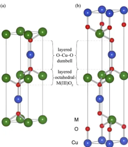
is shown in Fig.1. Each Cu atom is linearly coordinated by two oxygen atoms, forming O-Cu-O dumbbells parallel to the caxis. The oxygen atoms that terminate the dumbbells are also each coordinated to three Al atoms, oriented such that Al-centered octahedra form AlO2layers which lie
paral-lel to theabplane. Two alternative layer stacking sequences are possible to give hexagonal共space group P63/mmc with
ABABAB stacking兲 共Ref. 19兲or rhombohedral共space group R3-mhwithABCABC stacking兲 共Ref.20兲 polymorphs. The early work on CuAlO2was followed by study of the closely
related oxides CuGaO2 共Refs. 22and 23兲and CuInO2.24–26
The latter is of particular interest as it is amenable to bipolar doping.27The band gap of CuAlO2was originally reported to
be 3.5 eV.15,16 Most surprisingly the measured optical gaps
for the CuMO2 delafossites discussed above were found to
follow the order CuAlO2共3.5 eV兲⬍CuGaO2共3.6 eV兲 ⬍CuInO2共3.9 eV兲. Subsequent theoretical work established that delafossites are indeed indirect-gap materials and that both the direct and the lower energy indirect gaps follow the expected sequence CuAlO2⬎CuGaO2⬎CuInO2. The
from very low dipole intensity in the absorption spectrum even above the direct threshold for CuInO2.27 The actual
magnitude of the indirect gap in CuAlO2remains
controver-sial. The experimental value of 1.8 eV which was suggested by Yanagiet al.16 has been called into question on the basis
of calculations using a hybrid Hartree-Fock density-functional Hamiltonian. These calculations are expected to give reasonable estimates of absolute values of bulk band gaps28 and suggest an indirect gap of 3.9 eV for CuAlO
2.29
However, this value is in turn probably too high.
CuCrO2 has been the focus of recent interest as a further
p-type TCO. It remains tolerably transparent in the visible region despite the fact that there must be dipole forbidden 3d→3d excitations centered on Cr in the visible region. Hole mobilities of 11 cm2V−1s−1 have been measured with carrier concentrations around 4.75⫻1017 cm−3 in thin-film
material doped by native defects.30 Higher levels of p-type
doping can be achieved by substitution of Cr3+with divalent
cations. Mg-doped CuCrO2 has the highest reported p-type conduction of any TCO.31 Other divalent dopants such as
Ca,32 Ni,33 and Cd 共Ref. 34兲 have also been studied. The
onset of strong optical absorption in CuCrO2 occurs at
around 3 eV.34–36 Early photoelectrochemical experiments
suggested that the onset was associated with an indirect gap of 3.08 eV 共Ref. 35兲 but more recent absorption measure-ments are consistent with a direct gap of 3.10 eV.31 Lower
energy indirect gaps of 1.28 eV共Ref.33兲and 1.45 eV共Ref.
30兲 have also been implicated. Recent theoretical work showed that as with the other delafossites the lowest energy band gap in 2H-CuCrO2is indeed indirect but that the
sepa-ration between the lowest energy direct and indirect gaps is only about 0.5 eV.37Taking this number in conjunction with
the experimental direct gap of 3.1 eV gives an estimate of 2.6 eV for the lowest energy indirect gap.
In the present paper we present a comprehensive study of the electronic structure of CuCrO2 using x-ray
photoemis-sion, x-ray absorption, and x-ray emission spectroscopies as probes of partial densities of states. The results are compared to band-structure calculations on CuCrO2.37 CuCrO2 is of
particular interest in the context of resonant inelastic x-ray scattering because of the presence of two different transition metals with widely separatedL edges. We find that distinct electronic excitations may be accessed by studying x-ray scattering at the CuL and CrL edges.
II. EXPERIMENT
Ceramic samples of CuCrO2 and CuCr0.98Mg0.02O2were prepared by solid-state reaction between CuO, Cr2O3, and 共for the doped sample兲MgO.31The oxides were ground in an
agate mortar and pestle, pressed into pellets with tungsten carbide dies, and sintered at 1200 ° C for 48 h with interme-diate regrinding and pelletization. The pellets were finally quenched into liquid nitrogen to give a phase pure materials whose x-ray diffraction patterns measured in a-2 diffrac-tometer contained only peaks associated with the rhombohe-dral R3 phase. Sample conductivity was measured over a temperature range between 300 and 200 K using a four-probe technique on rectangular bars cut from the pellets. The activation energy for conduction was found to be 0.29 eV for the nominally undoped sample and 0.04 eV for the 2% Mg-doped sample.
High-resolution x-ray photoemission spectra were mea-sured in a Scienta ESCA 300 spectrometer. This incorporates a rotating anode AlK␣ 共h= 1486.6 eV兲 x-ray source, a seven-crystal x-ray monochromator, and a 300 mm mean ra-dius spherical sector electron energy analyzer with parallel electron detection system. The x-ray source was ran with 200 mA emission current and 14 kV anode bias, while the ana-lyzer operated at 150 eV pass energy. Gaussian convolution of the analyzer resolution with a linewidth of 260 meV for the x-ray source gives an effective instrument resolution of 450 meV. Samples were cleaned in situ by annealing at 400 ° C. The C 1s to O 1s intensity ratio was reduced to below 1/100. Binding energies are referenced to the Fermi energy of a silver sample regularly used to calibrate the spec-trometer.
X-ray absorption and emission spectra were measured on two beam lines. Initial measurements on the CuL and OK edges were performed on beam line 7.0.1 at the Advanced Light Source 共ALS兲, Lawrence Berkeley National Labora-tory. This beam line is equipped with a spherical grating monochromator.38 Emission spectra were recorded using a
Nordgren-type grazing-incidence spherical grating spectrometer.39For resonant emission experiments, the beam
line was set to have an energy resolution of 500 meV at the OK edge and 1 eV at the CuL3 edge, and the emission
spectrometer was set to have a resolution of 350 meV for OKand 750 meV for CuL3edge spectra. Absorption
spec-tra were measured in total fluorescence yield共TFY兲and total electron yield 共TEY兲modes, although only TEY spectra are presented. For the absorption measurements, the beam line resolution was set to 200 meV for the OKedge and to 1 eV for the CuL3 edge. The absorption spectra were normalized
[image:2.609.70.275.63.297.2]to a reference current from a clean gold mesh positioned in FIG. 1. 共Color online兲Unit cells for the two polymorphs of the
the path of the photon beam. The energy scales of the OK absorption spectra were calibrated relative to the OK ab-sorption spectrum of NiO and the CuL emission spectra were calibrated relative to theL absorption spectrum of Cu metal. The OKemission spectra were calibrated to ZnL␣1,2 andL1emission lines of Zn metal in second order, and the
CuL-edge emission spectra were calibrated relative to me-tallic CuL␣1,2 and L1 emission spectra measured in first
order. The consistency of the calibrations in x-ray photo-emission spectroscopy 共XPS兲 and x-ray emission spectros-copy共XES兲to within 0.2 eV is demonstrated by the fact that the peak maximum in nonresonant CuL3 XES共
correspond-ing to the position of the peak maximum in the Cu 3dpartial density of states relative to the Cu 2p3/2 core hole兲 is at
929.45 eV⫾0.2 eV while the separation between the Cu 2p3/2core level and valence-band peak maxima共the latter
again corresponding to the position of the peak maximum in the Cu 3d partial density of states兲 in XPS is 929.65 eV⫾0.1 eV for CuCrO2.
Further experiments at the OKedge and CrLedge were performed at the soft x-ray undulator beam line X1B at the National Synchrotron Light Source共NSLS兲, Brookhaven Na-tional Laboratory, which is also equipped with aspherical grating monochromator and Nordgren-type grazing-incidence spherical grating spectrometer. In the resonant mode, the beam line was set to energy resolutions of 700 meV for the OKedge and 1.1 eV for the CrLedge, and the emission spectrometer was set to a resolution of 370 meV for the OKedge and 600 meV for the CrLedge. X-ray absorp-tion spectroscopy 共XAS兲 spectra were recorded in TEY mode by measuring the sample drain current and were nor-malized to the current from a reference Au coated mesh in the incident photon beam. The energy resolution was set at 190 meV for the OKedge and 220 meV for the CrLedge. The energy scale of the XAS measurements was calibrated using first and second-order diffraction TiLedge absorption features of rutile TiO2.
III. RESULTS AND DISCUSSION
A. X-ray photoemission and nonresonant x-ray emission spectra
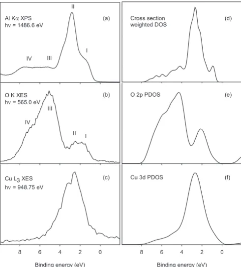
The experimental valence-band AlK␣ x-ray photoelec-tron spectrum of CuCrO2is shown in Fig.2along with OK
and CuL3x-ray emission spectra excited under nonresonant conditions with photons whose energies were well above the relevant core thresholds. For comparison with the experi-mental data we repeated the band-structure calculations we have recently performed on 2H-CuCrO2 for the 3R-CuCrO2
polymorph. Full details of the computational approach that was adopted are given in Ref.37. In outline, the calculations were performed using density-functional theory 共DFT兲 as embodied in the VASP code. The generalized gradient ap-proximation 共GGA兲 was used with correction for on-site Coulomb interactions 共the so-called GGA+U method兲. The Coulomb parameter U was assigned a value of 5.2 eV for Cu 3d states and 4.0 eV for Cr 3d states. These values are selected to give good agreement with valence-band photo-emission spectra of Cu2O and Cr2O3, respectively.37 The
ground state to emerge from these calculations involves an-tiferromagnetic ordering of spins on the Cr共III兲 sites along thecaxis so for the 3Rpolymorph it was necessary to use a 1⫻1⫻2 supercell. As expected, the calculated densities of states and bond lengths were virtually identical for 2H and 3R polymorphs.
The XPS data are compared with the cross-section-weighted density of states, while OK and CuL3 emission
spectra are compared with O 2p and Cu 3d partial densities of states respectively. Four features labeled I-IV may be identified in the experimental spectra. Reference to the band structure calculations shows that I and II relate to states of dominant Cu 3d atomic character while III and IV are asso-ciated with states of dominant O 2p character. In x-ray pho-toemission band II is the strongest component of the experi-mental valence-band spectrum and I appears as an ill resolved shoulder to low binding energy. Bands III and IV are found at higher binding energy and are also weaker than I but of comparable intensity to each other. The one-electron cross section for ionization of Cu 3d states is a factor of 20 bigger than for O 2p states under AlK␣excitation40 so that
the experimental spectrum is dominated by the Cu 3dpartial density of states even for bands III and IV. In OKshell x-ray emission the intensity distribution is reversed and I and II are
Binding energy (eV) 0 2 4 6 8
Binding energy (eV) 0 2 4 6 8 Al KαXPS hν= 1486.6 eV
O K XES hν= 565.0 eV
Cu L3 XES hν= 948.75 eV
(a)
(b)
(c) I II
III IV
I II III
IV
(d)
(e)
(f) Cross section
weighted DOS
O 2p PDOS
[image:3.609.314.559.68.338.2]Cu 3d PDOS
FIG. 2. Left hand panels:共a兲AlK␣excited valence-band x-ray photoemission,共b兲OKx-ray emission, and共c兲nonresonant CuL3 spectra of CuCrO2. The x-ray emission spectra have been shifted to
align with the AlK␣XPS and are presented on a binding-energy scale. Right hand panels:共d兲cross-section-weighted calculated den-sity of states broadened by 0.35 eV, 共e兲 calculated O 2p partial density of states broadened by 0.6 eV, and 共f兲 calculated Cu 3d partial density of states broadened by 1.2 eV for CuCrO2. The
much weaker than III and IV. There are also changes of relative intensity within the pairs I, II and III, IV. Specifically II loses intensity relative to I and IV relative to II. The fact that bands I and II appear at all in OK shell x-ray emission is a direct consequence of hybridization between Cu 3d and O 2p states which introduces O 2p character into states of nominal Cu 3d parentage. The hybridization is stronger for the states in band I than states in band II. This is largely a consequence of the local linear coordination of Cu. Within the linear O-Cu-O units the Cu 3dz
2
orbitals have-like sym-metry, the Cu 3dxzand 3dyzorbitals-like symmetry, and the
Cu 3dxyand Cu 3dx2−y2 orbitals␦-like symmetry. No mixing with O 2pstates is possible for the Cu 3d orbitals of␦ sym-metry, while the mixing for thestates is weaker than for states.38–41The observed intensity changes are therefore
con-sistent with the fact that the states in band I are -like whereas the␦andCu 3dstates contribute most strongly to band II.
Comparison between AlK␣ x-ray photoemission spectra of CuAlO2 共Ref. 41兲 and CuCrO2 关Fig. 3共a兲兴 superficially
suggests that Cr 3dstates are located in the upper part of the valence band between bands I and II, filling in the distinct dip between the two that is found in valence-band XPS of CuAlO2. However, the one-electron cross section for
ioniza-tion of Cr 3d states is only 0.18 kB, whereas the cross sec-tion for Cu 3d states is 1.2 kB.40 In addition the nominal
electron count is only three for Cr as compared to ten for Cu. As shown in Fig. 3共b兲 the cross-section-weighted contribu-tion of the Cr 3d partial density of states to the AlK␣ pho-toemission spectrum is negligible compared to the Cu 3d contribution. The differences in the photoemission spectra between CuAlO2 and CuCrO2 may instead be traced to
changes in the Cu 3d partial density of states when Al is replaced by Cr. In particular replacement of Al by Cr adds spectral weight to the upper part of the valence band. This is apparently via indirect interactions mediated by O, which interacts strongly with both Cu and Cr. It is also noticeable in the experimental spectra that the O 2p part of the valence band is broader for CuAlO2 than CuCrO2. Finally
replace-ment of Al by Cr results in pronounced changes in the region of valence-band satellites. For CuAlO2 a single weak
satel-lite labeled s1 in Fig.3共c兲is observed at a binding energy of 16 eV. This is at a similar energy to the satellite in valence region photoemission spectra of Cu2O which are associated
with Cu 3d84共sp兲1final states, where 4共sp兲1represents
exci-tation of a valence electron into the conduction band.42,43
The s1 satellite is also present in the photoemission spectrum of CuCrO2, but a second satellite labeled s2 in Fig. 3共d兲is
observed at a binding energy of just over 10 eV. This corre-sponds to the valence-band satellite in the photoemission spectrum of Cr2O3 associated with an unscreened 3d2 final
state.44,45
B. Resonant x-ray scattering and emission at the CuLedge
The x-ray absorption spectrum of CuCrO2 at the CuL3 edge is shown in Fig.4共a兲. The spectrum is dominated by a sharp peak with a maximum at 934.25 eV, although this is preceded by a very weak prepeak labeled p in the figure. The
prepeak is associated with Cu2+ 3d9states, i.e., holes in the
Cu 3d valence band.41 The position of the bottom of the
conduction band is shown as a vertical dashed line in this figure. The placement of this threshold is derived from the measured binding energy of 932.45 eV for the Cu 2p3/2core
Binding energy (eV)
0 2 4 6 8 10
CuAlO2
CuCrO2 Al Kα
Cu 3d PDOS
Cr 3d PDOS
Weighted Cr 3d PDOS CuCrO2
x 20
CuAlO2
CuCrO2
Binding energy (eV)
8 10 12 14 16 18 20
s1
s1 s2
(a)
(b)
(c)
[image:4.609.349.519.70.565.2](d)
FIG. 3. 共Color online兲 共a兲Valence-band AlK␣XPS of CuCrO2
compared to that of CuAlO2. The spectra have been subject to small shifts so that the zero in the binding-energy scale coincides with the top of the valence band. 共b兲 Cu 3d and Cr 3d calculated partial densities of states for CuCrO2, also showing the weighted partial
density of states for the Cr 3dstates obtained by multiplying the raw partial density of states共PDOS兲by共Cr 3d兲/共Cu 3d兲, where
are one-electron ionization cross sections. 共c兲 Valence satellite region in AlK␣ XPS of CuAlO2. 共d兲 Valence satellite region in
level in XPS. Assuming that the Fermi level is 0.29 eV above the valence-band maximum, as implied by the measured ac-tivation energy for conduction, this fixes the edge of the valence band 共932.45 eV− 0.29 eV兲= 932.16 eV above the
Cu 2p3/2 core level. This value must be corrected for the estimated band gap of 2.6 eV for CuCrO2 to give a
place-ment of the bottom of the conduction band 共932.16 eV + 2.6 eV兲= 934.76 eV above the Cu 2p3/2 core level. The
peak maximum in the absorption spectrum is seen to lie be-low the estimated position of the bottom of the conduction band. This implies that the absorption onset is dominated by a strong Coulomb attraction between the excited electron and the core hole to give a core-hole exciton. Very similar behav-ior has recently been seen for Cu2O.46
Emission spectra excited over a range of photon energies between 933.25 and 935.25 eV are shown in Fig. 4共b兲. A single broad emission feature is observed which moves to higher energy with increasing exciting photon energy for the three lowest excitation energies. These spectra are transposed onto an energy-loss scale in Fig.4共c兲. It is now apparent that the movement seen in Fig. 4共b兲 corresponds to a constant energy loss of 4.7 eV⫾0.2 eV. This lost energy is very similar to that for inelastic loss features found at the CuL3 edge for Cu2O 共Ref. 46兲 共where the value is 4.5 eV兲 and CuAlO2 共Ref. 41兲 共where the value is 5.4 eV兲. As in these
materials the loss feature is assigned to onsite interband ex-citations from Cu 3d states at the top of the valence band into empty conduction-band states which have both Cu 3d and Cu 4scharacters. Both 3d→4sand 3d→3d excitations are allowed by the ⌬l= 0 ,⫾2 selection that governs elec-tronic Raman scattering although the 3d→3d channel is likely to dominate the spectra because the matrix elements between core 2p states and valence 4s states are much smaller than corresponding matrix elements between 2p and 3d states.47,48 It is interesting to note that resonant inelastic
x-ray scattering is only observed for incident photon energies in the excitonic regime.
C. Resonant x-ray scattering and emission at OKand CrL
edges
The OKand CrLedges lie within 60 eV of each other so it is instructive to examine absorption and nonresonant emis-sion spectra which encompass both edges. As shown in Fig.
5 CrLabsorption is much stronger than OKabsorption but CrLshell x-ray emission is much weaker than OKemission under nonresonant condition with excitation ath= 611 eV. This is attributed to the fact that the fluorescence yield in CrLshell decay is much lower than the corresponding yield for OKshell decay due to the relatively higher efficiency of Auger decay processes. For this reason it was difficult to gather CrLemission data with good signal-to-noise ratio.
The OKabsorption spectrum is shown in greater detail in Fig. 6共a兲. As in Fig. 4 the position of the bottom of the conduction band relative to the peak maximum in the O 1s core level as estimated from the O 1score-level binding en-ergy is also shown in the figure. In contrast to the CuL absorption spectrum the peak maximum in the OK absorp-tion spectrum does not lie below the conducabsorp-tion-band mini-mum, i.e., there is no indication of formation of a true core-hole exciton. However, comparison between the experimental absorption spectrum and the calculated empty O 2ppartial density of states shows that the distinct peak at
Cu L 3 RIXS
Photon Energy (eV)
924 928 932 936 940 944
hν= 935.25eV
hν= 934.75eV
hν= 934.25eV
hν= 933.75eV
hν= 933.25eV
Cu L 3 RIXS
Energy Loss (eV)
-4 0 4 8 12
hν= 933.25eV
hν= 933.75eV
hν= 934.25eV hν= 934.75eV hν= 935.25eV
TEY Cu L3 XAS (a)
(b)
[image:5.609.90.254.66.576.2](c) p
FIG. 4.共a兲Total electron yield CuL3x-ray absorption spectrum
of CuCrO2. The vertical dashed line shows the location of the bot-tom of the conduction band derived from analysis of XPS data. The diamonds show the energies used for excitation of x-ray emission spectra.共b兲 CuL3 x-ray emission spectra excited at the emission
the threshold is not a simple feature of the density of states. It therefore appears that the core-hole potential has a strong effect on the absorption spectrum leading to a resonance em-bedded in the bottom of the conduction band.
Resonant OK x-ray emission spectra excited over the range of photon energies close to the OK edge threshold highlighted in Fig. 6共a兲 are shown in Fig. 6共b兲. Again in contrast to the CuL edge there is no obvious movement in the spectral features with varying photon energy. Thus a simple emission process seems to dominate over resonant inelastic x-ray scattering. This again mirrors results found for CuAlO2 共Ref.41兲and Cu2O.46
The CrL edges present a more complex story. The CrL absorption spectrum is shown in Fig. 7共a兲. The spectrum is very similar to that of Cr2O3 and is dominated by the
sepa-ration of about 9.5 eV betweenL3 andL2 components with additional fine structure arising from multiplet effects arising from addition of an extra electron to the 3d3 configuration. The separation between the CrL3 and CrL2 onsets is
com-parable to the width of the valence band. The emission spec-tra shown in Fig.7共b兲show pronounced shifts in peak posi-tions with exciting photon energy. However, when the spectra are transposed onto an energy-loss scale as in Fig.
7共c兲 it becomes apparent that a sharp and well-defined loss peak appears at an energy loss of 2.1 eV⫾0.2 eV. An elas-tic peak appears as a shoulder on the low energy-loss side of this peak and there are also indications of a broader loss feature at 10 eV, probably associated with charge-transfer excitations The low energy 2.1 eV loss feature arises from ligand field excitations of Cr3+. The Cr3+ion in an octahedral
environment has at2g3 configuration with a ground state4A2g.
The optical-absorption spectrum of Cr2O3 and other
com-pounds with Cr3+in an octahedral environment contain two
spin-allowed 共but dipole forbidden兲 bands associated with the 4T2gand4T1gstates of the excitedt2g
2
eg 1
configuration, as well as spin-forbidden transitions. In electronic Raman scat-tering, the components of the polarizability tensor span irre-ducible representations A1g+Eg+T2g so that the transition 4
A2g→4T1gis allowed but4A2g→4T2gis formally forbidden
in a coherent scattering process. The Raman-scattering cross section contains a product of dipole matrix elements con-necting initial and final states to a common intermediate state. It might therefore be assumed that since the dipole operator transforms as T1u and the direct product T1u⫻T1u
=A1g+Eg+T2g+关T1g兴, transitions mediated byT1g should be
allowed. This would include the excitation 4A2g→4T2g and indeed Matsubaraet al.49have argued thatT2gexcited states
are accessible. However,关T1g兴constitutes the part of the
di-rect product antisymmetric with respect to particle exchange. Owing to the fact that photons are bosons T1g should be
excluded in formulation of selection rules. Thus the single observed band is tentatively assigned to the allowed 4A2g
→4T
1g excitation. The corresponding energy of this
excita-tion in Cr2O3 is 2.6 eV.50–52 The lower value for CuCrO 2
may reflect reduced Cr-O covalency due to the competition
520 540 560 580 600
Photon energy (eV)
520 540 560 580 600
Cr L3
Cr L2 O K
Cr L3,2
O K TEY XAS
XES hν= 611 eV
(a)
[image:6.609.352.520.64.346.2](b)
FIG. 5. 共a兲X-ray absorption spectra of CuCrO2across the OK and CrLedges measured in the total electron yield mode.共b兲OK and CrL emission spectra measured under excitation by photons withh= 611 eV.
Photon energy (eV)
516 520 524 528 532 536 540 544
O K TEY XAS
OK RXES
hν= 549.5 eV
hν= 542.3 eV
hν= 533.9 eV
hν= 532.2 eV
hν= 531.8 eV
hν= 531.3 eV (a)
(b)
FIG. 6. 共a兲OKx-ray absorption spectrum of CuCrO2measured
[image:6.609.89.256.66.339.2]from formation of short and strong Cu-O bonds. The energy-loss spectra for CuCrO2 are similar to those of Cr2O3 as
reported by Matsubara et al.49 who despite their theoretical
analysis observed a single 3d→3d loss peak. These authors analyzed the loss spectra in terms of a model Hamiltonian with a ligand field splitting parameter 10Dq= 1.3 eV and a Coulomb repulsion parameter between 3d electrons Udd
= 5.5 eV. The value for 10Dq is much lower than values around 2.06 eV obtained from optical-absorption measure-ments on thin Cr2O3films.50–52
Comparison between nonresonant CrL shell x-ray emis-sion is complicated by the close proximity of the Cr 2p3/2
and Cr 2p1/2 levels seen in both x-ray absorption and core level x-ray photoemission关Fig.8共a兲兴. Using a value for the spin-orbit splitting of the core levels from XPS it is however possible to “spin-orbit strip” the nonresonant CrL emission spectrum shown in Fig. 8共b兲 to give the L3 spectrum. The
results of this procedure are shown in Fig. 8共c兲 along with the broadened Cr 3d partial density of states derived from the band-structure calculation. Although the shape of the ex-perimental spectral profile matches that of the computed Cr 3d partial density of states the CrL emission extends
Energy Loss (eV)
-5 0 5 10 15 20 25
Photon Energy (eV)
550 560 570 580 590 600 610
Cr L XAS
Cr L RIXS
Cr L RIXS hν= 587.6 eV
hν = 585.5 eV
hν= 577.6 eV
hν= 576.5 eV
hν= 587.6 eV
hν = 585.5 eV
hν= 577.6 eV
hν= 576.5 eV (a)
(b)
[image:7.609.354.515.69.451.2](c)
FIG. 7.共a兲CrLx-ray absorption spectrum of CuCrO2measured
in the total electron yield mode. The dashed vertical lines show the position of the bottom of the conduction band derived from analysis of XPS data while the diamonds show the energies used for excita-tion of x-ray emission spectra.共b兲Emission spectra excited at the photon energies indicated.共c兲Spectra as in共b兲above but plotted on an energy-loss scale. This allows identification of a sharp loss fea-ture at ca. 2.1 eV, together with a broader loss feafea-ture at ca. 10 eV.
550 560 570 580 590 600
Photon energy (eV)
550 560 570 580 590 600
Cr L3
Cr L2
Cr L XES
hν= 611 eV
Cr L3XES
Spin-orbit stripped Binding energy (eV)
560 570 580 590 600
Cr 2p1/2 Cr 2p3/2
* Cu LMM (a)
(b)
(c)
Al KαXPS
FIG. 8. 共a兲 Cr 2p structure in the AlK␣ X-ray photoelectron spectrum, of CuCrO2. The Cr core lines overlap with CuLMM Auger structure: the dotted line shows part of the Auger spectrum of Cu2O. 共b兲 Nonresonant CrL x-ray emission spectrum of CuCrO2 excited at h= 611 eV showing L3and L2 components. 共c兲 Solid
line: L3 emission spectrum following spin-orbit stripping of the
spectrum in共b兲assuming a spin-orbit coupling constant of 9.7 eV. Dotted line: calculated Cr 3d partial density of states in CuCrO2
[image:7.609.90.254.70.561.2]down to lower energy than predicted by the band-structure calculation. This must be due in part to unresolved Cr satel-lite structure. Although the satelsatel-lite is relatively weak in AlK␣valence-band photoemission, it will have greater rela-tive intensity in CrLXES, which of course selects out Cr 3d spectral weight.
D. Shift in Fermi level with doping
The valence-band photoemission spectrum of CuCrO2 in
Fig. 2 showed that the Fermi level in nominally undoped CuCrO2 lays just above the valence-band edge in the lower
part of the bulk band gap, as to be expected for a p-type oxide. The valence-band AlK␣ photoemission onsets for nominally undoped CuCrO2 and 2% Mg-doped CuCrO2 共CuCr0.98Mg0.02O2兲 are shown in greater detail in Fig. 9共a兲.
There is a well-defined shift to low binding energy with dop-ing, similar to that found for K doping in SrCu2O2.53 In
nominally undoped CuCrO2 the peak maximum in the
va-lence band is found at 2.80 eV⫾0.05 eV, while for the Mg doped sample the maximum is at 2.50 eV⫾0.05 eV. The downward shift of 0.30 eV is therefore close to the change in
activation energy for conduction inferred from four-probe conductivity measurements, where a decrease from 0.29 to 0.04 eV共i.e., 0.25 eV兲is found. The photoemission measure-ments therefore confirm that the Fermi level moves toward the valence-band edge with Mg doping. The shift in the valence-band structure is accompanied by corresponding shifts in core level binding energies. Thus Fig. 9共b兲 shows the Cu 2p3/2peaks for nominally undoped and 2% Mg-doped
CuCrO2. The peak maximum shifts from
932.45 eV⫾0.05 eV to 932.20 eV⫾0.05 eV with Mg doping, again consistent with a change in the activation en-ergy for conduction of 0.25 eV.
IV. CONCLUDING REMARKS
The electronic structure of CuCrO2has been found to be
very similar to that of other Cu共I兲oxides where Cu is found in a linear coordination environment. It is difficult to pin-point the Cr 3d states experimentally, but comparison to band-structure calculations suggest that the Cr 3d states straddle most of the valence band and hybridize strongly with O 2p states at the bottom of the valence band. The significant Cr 3d contribution to the top of the valence band suggests that the holes introduced into CuCrO2 by p-type
doping are partially delocalized onto Cr. This possibly ac-counts for the higher conductivity of CuCrO2 as compared
with CuAlO2. The presence of two distinct transition-metal
ions in this ternary oxide has allowed us to use resonant inelastic x-ray scattering at the two metal L edges to probe site selective electronic excitations. Scattering at the CuL edge excites onsite interband excitations very similar to those seen in CuAlO2and Cu2O, while scattering at the CrL edge results in excitation of 3d→3dtransitions arising from ligand field splitting of the Cr 3dlevels. This selectivity can-not be obtained in conventional optical experiments.
ACKNOWLEDGMENTS
Experimental work on transparent conducting oxides in Oxford is supported under EPSRC Grant No. GR/S94148 and the NCESS Facility by Grant Scienta XPS facility by EPSRC Grant No. EP/E025722/1. The Boston University program is supported in part by the U.S. Department of En-ergy under Contract No. DE-FG02-98ER45680 and in part by the Donors of the American Chemical Society Petroleum Research Fund. The Advanced Light Source is supported by the Director, Office of Science, Office of Basic Energy Sci-ences, of the U.S. Department of Energy under Contract No. DE-AC02-05CH11231. Use of the National Synchrotron Light Source, Brookhaven National Laboratory, was sup-ported by the U.S. Department of Energy, Office of Science, Office of Basic Energy Sciences, under Contract No. DE-AC02-98CH10886. The Trinity College Dublin program is funded by Science Foundation Ireland under Grant No. 06/IN.1/I92.
Binding energy (eV)
930 931 932 933 934 935
-1 0 1 2 3 4
Valence band
Cu 2p3/2
Nominally undoped
2% Mg doped (a)
[image:8.609.90.254.64.373.2](b)
FIG. 9. 共a兲Valence-band thresholds in AlK␣ excited valence region photoemission spectra of nominally undoped CuCrO2 and
*Corresponding author: [email protected]
†Present address: National Renewable Energy Laboratory, Golden,
Colorado 80401, USA
1H. L. Hartnagel, A. L. Dawar, A. K. Jain, and C. Jagadish,
Semi-conducting Transparent Thin Films共IOP, Bristol, 1995兲.
2P. D. C. King, T. D. Veal, D. J. Payne, A. Bourlange, R. G.
Egdell, and C. F. McConville Phys. Rev. Lett. 101, 116808
共2008兲.
3For a discussion of n-type doping in In
2O3, see, e.g., C. G.
Granqvist and A. Hultåker, Thin Solid Films 411, 1共2002兲.
4A. Tsukazaki, H. Saito, K. Tamura, M. Ohtani, H. Koinuma, M.
Sumiya, S. Fuke, T. Fukumura, and M. Kawasaki, Appl. Phys. Lett. 81, 235共2002兲.
5S. B. Zhang, S.-H. Wei, and A. Zunger, Phys. Rev. B 63, 075205 共2001兲.
6T. Yamamoto and H. K. Yoshida, Jpn. J. Appl. Phys., Part 2 38,
L166共1999兲.
7M. Joseph, H. Tabata, and T. Kawai, Jpn. J. Appl. Phys., Part 2 38, L1205共1999兲.
8A. Tsukazaki, A. Ohtomo, T. Onuma, M. Ohtani, T. Makino, M.
Sumiya, K. Ohtani, S. F. Chichibu, S. Fuke, Y. Segawa, H.
Ohno, H. Koinuma and M. Kawasaki, Nature Mater. 4, 42
共2005兲.
9T. Yamamoto and H. Katayama-Yoshida, Jpn. J. Appl. Phys.,
Part 2 38, L166共1999兲.
10P. Erhart, A. Klein, R. G. Egdell, and K. Albe, Phys. Rev. B 75,
153205共2007兲.
11A. Walsh, J. L. F. Da Silva, S.-H. Wei, C. Körber, A. Klein, L. F.
J. Piper, A. DeMasi, K. E. Smith, G. Panaccione, P. Torelli, D. J. Payne, A. Bourlange, and R. G. Egdell, Phys. Rev. Lett. 100, 167402共2008兲.
12F. Fuchs and F. Bechstedt, Phys. Rev. B 77, 155107共2008兲. 13A. Walsh, J. L. F. Da Silva, and S.-H. Wei, Phys. Rev. B 78,
075211共2008兲.
14S. Nikitine, J. B. Grun, and M. Sieskind, J. Phys. Chem. Solids 17, 292共1961兲.
15H. Kawazoe, M. Yasukawa, H. Hyodo, M. Kurita, H. M. Yanagi,
and H. Hosono, Nature 389, 939共1997兲.
16H. Yanagi, S. Inoue, K. Ueda, H. Kawazoe, H. Hosono, and N.
Hamada, J. Appl. Phys. 88, 4159共2000兲.
17H. Katayama-Yoshida, K. Sato, H. Kizaki, H. Funashima, I.
Ha-mada, T. Fukushima, V. A. Dinh, and M. Toyoda, Appl. Phys. A
89, 19共2007兲.
18I. Hamada and H. Katayama-Yoshida, Physica B 376-377, 808 共2006兲.
19O. Crottaz and F. Kubel, Z. Kristallogr. 211, 481共1966兲. 20O. Crottaz and F. Kubel, Z. Kristallogr. 211, 482共1996兲. 21O. Crottaz, F. Kubel, and H. Schmid, J. Solid State Chem. 122,
247共1996兲.
22K. Ueda, T. Hase, H. Yanagi, H. Kawazoe, H. Hosono, H. Ohta,
M. Orita, and M. Hirano, J. Appl. Phys. 89, 1790共2001兲.
23H. Yanagi, H. Kawazoe, A. Kudo, M. Yasukawa, and H. Hosono,
J. Electroceram. 4, 407共2000兲.
24H. Yanagi, T. Hase, S. Ibuki, K. Ueda, and H. Hosono, Appl.
Phys. Lett. 78, 1583共2001兲.
25H. Yanagi, K. Veda, H. Ohta, M. Orita, M. Hirano, and H.
Hosono, Solid State Commun. 121, 15共2001兲.
26L. Liu, K. Bai, H. Gong, and P. Wu, Phys. Rev. B 72, 125204 共2005兲.
27X. L. Nie, S.-H. Wei, and S. B. Zhang, Phys. Rev. Lett. 88,
066405共2002兲.
28J. Muscat, A. Wander, and N. M. Harrison, Chem. Phys. Lett. 342, 397共2001兲.
29J. Robertson, P. Peacock, M. Towler, and R. Needs, Thin Solid
Films 411, 96共2002兲.
30S. Mahapatra and S. Shivashankar, Chem. Vap. Deposition 9,
238共2003兲.
31R. Nagarajan, A. Draeseke, A. Sleight, and J. Tate, J. Appl. Phys. 89, 8022共2001兲.
32H. Huang, C. F. Zhu, and W. Liu, Chin. J. Chem. Phys. 17, 161 共2004兲.
33S. Y. Zheng, G. S. Jiang, J. R. Su, and C. F. Zhan, Mater. Lett. 60, 3871共2006兲.
34M. Lalic and J. Mestnik-Filho, J. Phys.: Condens. Matter 18,
1619共2006兲.
35F. A. Benko and F. P. Koffyberg, Mater. Res. Bull. 21, 753 共1986兲.
36D. Li, X. Fang, Z. Deng, S. Zhou, R. Tao, W. Dong, T. Wang, Y.
Zhou, G. Meng, and X. Zhu, J. Phys. D 40, 4910共2007兲.
37D. O. Scanlon, A. Walsh, B. J. Morgan, G. W. Watson, D. J.
Payne, and R. G. Egdell, Phys. Rev. B 79, 035101共2009兲.
38J. Nordgren and R. Nyholm, Nucl. Instrum. Methods Phys. Res.
A 246, 242共1986兲.
39J. Nordgren, G. Bray, S. Cramm, R. Nyholm, J. E. Rubensson,
and N. Wassdahl, Rev. Sci. Instrum. 60, 1690共1989兲.
40J. J. Yeh and I. Lindau, At. Data Nucl. Data Tables 32, 1共1985兲. 41D. J. Aston, D. J. Payne, A. J. H. Green, R. G. Egdell, D. S. L.
Law, J. Guo, P. A. Glans, T. Learmonth, and K. E. Smith, Phys. Rev. B 72, 195115共2005兲.
42J. Ghijsen, L. H. Tjeng, H. Eskes, G. A. Sawatzky, and R. L.
Johnson, Phys. Rev. B 42, 2268共1990兲.
43J. P. Hu, D. J. Payne, R. G. Egdell, N. M. Harrison, and V. R.
Dhanak, Chem. Phys. Lett. 450, 39共2007兲.
44D. E. Eastman and J. L. Freeouf, Phys. Rev. Lett. 34, 395 共1975兲.
45R. Zimmermann, P. Steiner, and S. Hüfner, J. Electron Spectrosc.
Relat. Phenom. 78, 49共1996兲.
46J. P. Hu, D. J. Payne, R. G. Egdell, P.-A. Glans, T. Learmonth, K.
E. Smith, J. Guo, and N. M. Harrison, Phys. Rev. B 77, 155115
共2008兲.
47U. Fano and J. W. Cooper, Rev. Mod. Phys. 40, 441共1968兲. 48M. Grioni, J. B. Goedkoop, R. Schoorl, F. M. F. deGroot, J. C.
Fuggle, F. Schafers, E. E. Koch, G. Rossi, J. M. Esteva, and R. C. Karnatak, Phys. Rev. B 39, 1541共1989兲.
49M. Matsubara, T. Uozumi, A. Kotani, Y. Harad, and S. Shin, J.
Phys. Soc. Jpn. 71, 347共2002兲.
50D. S. McClure, J. Chem. Phys. 38, 2289共1963兲.
51C. M. Mo, W. L. Cai, G. Chen, X. M. Li, and L. Zhang, J. Phys.:
Condens. Matter 9, 6103共1997兲.
52M. G. Brik, N. M. Avram, and C. N. Avram, Solid State
Com-mun. 132, 831共2004兲.
53C. C. B. Lynch, R. G. Egdell, and D. S. L. Law, Chem. Phys.