371XXC
VECTOR NETWORK ANALYZER
MAINTENANCE MANUAL
P/N: 10410-00236 490 JARVIS DRIVElMORGAN HILL, CA 95037-2809
WARRANTY
The ANRITSU product(s) listed on the title page is (are) warranted against defects in materials and workmanship for three years from the date of shipment.
ANRITSU’s obligation covers repairing or replacing products which prove to be defective during the warranty period. Buyers shall prepay transportation charges for equipment returned to ANRITSU for warranty repairs. Obligation is limited to the original purchaser. ANRITSU is not liable for con-sequential damages.
LIMITATION OF WARRANTY
The foregoing warranty does not apply to ANRITSU connectors that have failed due to normal wear. Also, the warranty does not apply to defects resulting from improper or inadequate maintenance by the Buyer, unauthorized modification or misuse, or operation outside of the environmental specifi-cations of the product. No other warranty is expressed or implied, and the remedies provided herein are the Buyer’s sole and exclusive remedies.
TRADEMARK ACKNOWLEDGEMENTS
V Connector and K Connector are registered trademarks of ANRITSUCompany. Ink Jet and Think Jet are registered trademarks of Hewlett-Packard Co. MS-DOS and Windows are a registered trademarks of Microsoft Corporation. Acrobat is a registered trademark of Adobe CorporationNOTICE
ANRITSU Company has prepared this manual for use by ANRITSU Company personnel and cus-tomers as a guide for the proper installation, operation and maintenance of ANRITSU Company equipment and computer programs. The drawings, specifications, and information contained herein are the property of ANRITSU Company, and any unauthorized use or disclosure of these drawings, specifications, and information is prohibited; they shall not be reproduced, copied, or used in whole or in part as the basis for manufacture or sale of the equipment or software programs without the prior written consent of WILTRON Company.
Table of Contents
Chapter 1 — General Service Information
This chapter provides a general description of Series 371XXC Vector Network Analyzer systems, sys-tem serial numbers, and frequency ranges. It explains the level of maintenance covered in this man-ual and the service strategy used throughout this manman-ual. It also contains static-sensitive component handling precautions and a list of recommended test equipment.
Chapter 2 — Replaceable Parts
This chapter lists all replaceable subassemblies and components for all 371XXC models. It explains the ANRITSU exchange assembly program and provides parts ordering information.
Chapter 3 — Operational Tests
This chapter contains procedures that provide a means of fully testing the 371XXC VNA system for proper operation and signal stability. These tests are intended to be used as a periodic check of the operational functionality of the 371XXC.
Chapter 4 — Performance Verification Procedures
This chapter provides detailed procedures for verifying that the performance of the 371XXC meets minimum performance standards.
Chapter 5 — Troubleshooting
This chapter provides information for troubleshooting Series 371XXC Vector Network Analyzer sys-tems. The troubleshooting procedures contained in this chapter support fault isolation down to a re-placeable subassembly.
Chapter 6 — Adjustments
This chapter provides adjustment procedures for all models of Series 371XXC Vector Network Ana-lyzer systems. These procedures are used after replacement or repair of one or more critical subas-semblies, or as indicated by the Performance Verification Procedures contained in Chapter 4.
Chapter 7 — System Description
This chapter provides descriptions of the functional operation of the major assemblies contained in Series 371XXC Vector Network Analyzer systems. The operation of all major circuit blocks is de-scribed so that the reader may better understand the function of each assembly as part of the overall operation.
Chapter 8 — Removal and Replacement Procedures
This chapter describes how to gain access to all of the major assemblies and major parts for troubleshooting and/or replacement.
Appendix A — Diagnostic Menus
This appendix contains descriptions and usage information for the Diagnostic Menus that are avail-able via the front panel Option Menu key.
Appendix B — Error Codes/Messages
This appendix contains a listing of the Error Codes/Messages. Also included is a description of the in-formation fields that are part of the error messages.
Appendix C — Connector Maintenance Check Procedures
This appendix contains procedures and information needed to perform maintenance checks (includ-ing pin-depth measurements) for the connectors on all ANRITSU supplied Calibration/Verification Kit components, Through-cables, and other associated RF/microwave components.
Appendix D — Performance Specifications
Appendix E — Millimeter Wave Instructions
This appendix provides service instructions for the 371XXC Millimeter Wave System. The informa-tion is specific to the 371XXC and is intended to supplement the common service instrucinforma-tions con-tained in the other parts of this manual.
Appendix F — SM5235 and SM5392 Instructions
This appendix contains operation, specification, and adjustment information for the SM5235 and SM5392 S-Parameter test sets.
Table of Contents
Chapter 1 General Information
1-1 SCOPE OF MANUAL · · · 1-3 1-2 INTRODUCTION · · · 1-3 1-3 ONLINE MANUALS · · · 1-3 1-4 IDENTIFICATION NUMBER · · · 1-3 1-5 SYSTEM DESCRIPTION · · · 1-4 1-6 RELATED MANUALS· · · 1-4 1-7 OPTIONS · · · 1-4 1-8 SERVICE STRATEGY · · · 1-4 Functional Assembly Level Troubleshooting · · · 1-5 Internal Hardware Adjustments and Calibrations · · · 1-5 Internal Service Log · · · 1-5 System Test/ Certification · · · 1-5 Preventive Service · · · 1-6 Servicing Specially Modified Instruments · · · 1-6 1-9 SERVICE SUPPORT INFORMATION · · · 1-6 Technical Support · · · 1-6 Service Software · · · 1-7 Test Fixtures/ Aids · · · 1-7 Failed Assembly Exchange Program · · · 1-7 1-10 RECOMMENDED TEST EQUIPMENT · · · 1-8 1-11 STATIC SENSITIVE COMPONENT
HANDLING PROCEDURES · · · 1-9 1-12 SERVICE CENTERS · · · 1-9 1-13 PERFORMANCE SPECIFICATIONS · · · 1-9
Chapter 2 Replaceable Parts
2-1 INTRODUCTION · · · 2-3 2-2 EXCHANGE ASSEMBLY PROGRAM · · · 2-3 2-3 REPLACEABLE SUBASSEMBLIES AND PARTS · · · 2-3 2-4 PARTS ORDERING INFORMATION · · · 2-4
Chapter 3 Operational Tests
3-1 INTRODUCTION · · · 3-3 3-2 CHECKING THE SERVICE LOG · · · 3-4 3-3 SELF TEST · · · 3-5 3-4 PERIPHERALS AND INTERFACES TESTS · · · 3-6 Display Test· · · 3-6 Front Panel Test · · · 3-7 External Keyboard Interface Test · · · 3-7 Printer Interface Test · · · 3-7 GPIB Interface Test · · · 3-9
Chapter 4 Performance Verification
4-1 INTRODUCTION · · · 4-3 4-2 CALIBRATION AND MEASUREMENT CONDITIONS · · · · 4-3 Standard Conditions · · · 4-3 Special Precautions· · · 4-4 4-3 PERFORMANCE VERIFICATION PROCEDURE · · · 4-4 Noise Floor/Receiver Dynamic Range Test · · · 4-5 Compression Test for 37147C, 37169C · · · 4-9
Chapter 5 Troubleshooting
5-1 INTRODUCTION · · · 5-3 5-2 ASSOCIATED INFORMATION IN THIS MANUAL · · · 5-4 5-3 RECOMMENDED TEST EQUIPMENT · · · 5-4 5-4 IF SYSTEM DOES NOT POWER-UP · · · 5-4 Line Source and Interface Checks · · · 5-4 Power Supply Voltages Check · · · 5-4 Power Supply Module Check· · · 5-6 5-5 IF SYSTEM DOES NOT BOOT-UP· · · 5-7 Boot-up Process Sequence · · · 5-7 Troubleshooting Boot-up Problems · · · 5-8 Hard Disk Problem 1 · · · 5-8 Hard Disk Problem 2 · · · 5-9 Floppy Disk Problems · · · 5-9 Screen Display Problems· · · 5-9
Phase Lock Error Codes (6000 Series) · · · 5-11 Service Log Snap Shot Data · · · 5-13 5-7 SIGNAL SOURCE, TEST SET, AND RECEIVER PROBLEMS 5-13 Signal Source Phase Lock Loop Assemblies · · · 5-14 Signal Source/Test Set Module Error Codes · · · 5-14 Isolation Procedures · · · 5-16 5-8 IF A PERIPHERALS/ INTERFACE TEST FAILED · · · 5-18 LCD Display Test Failures: · · · 5-18 Front Panel Test Failures: · · · 5-18 External Keyboard Interface Test Failures: · · · 5-18 Printer Interface Test Failures: · · · 5-19 GPIB Interface Test Failures: · · · 5-19 5-9 IF MEASUREMENTS ARE IN QUESTION · · · 5-19 Measurement Conditions Check List · · · 5-19
Chapter 6 Adjustments
6-1 INTRODUCTION · · · 6-3 6-2 LO1 CALIBRATION · · · 6-3 Calibration Procedure · · · 6-3 Post Calibration Actions · · · 6-4 6-3 LO 2 CALIBRATION · · · 6-4 Calibration Procedure · · · 6-4 Post Calibration Actions · · · 6-5 6-4 FREQUENCY CALIBRATION · · · 6-5 Calibration Procedure · · · 6-6 Post Calibration Actions · · · 6-7 6-5 RF POWER/ALC CALIBRATION· · · 6-8 Calibration Procedure · · · 6-8 Post Calibration Actions · · · 6-10 6-6 SOURCE LOCK THRESHOLD CALIBRATION · · · 6-11
Chapter 7 System Description
7-1 INTRODUCTION · · · 7-3 7-2 SYSTEM OVERVIEW · · · 7-3
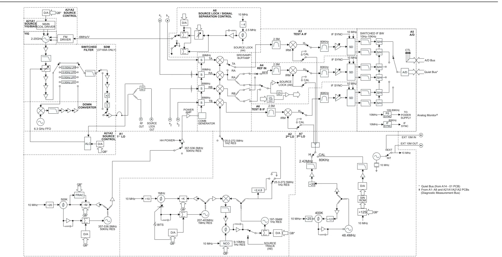
7-3 ANALOG SUBSYSTEM ASSEMBLIES · · · 7-7 Signal Source Module · · · 7-7 Test Set Module· · · 7-8 Receiver Module · · · 7-9 A8, Source Lock/ Signal Separation and Control PCB · · · 7-10 IF Section · · · 7-10 A7 PCB, LO3 · · · 7-10 A5 A/D Converter PCB · · · 7-11 7-4 DIGITAL SUBSYSTEM ASSEMBLIES · · · 7-12 A9 Main Processor PCB Assembly · · · 7-12 A7 PCB, 10 MHz Time Base· · · 7-13 A13 I/O Interface #1 PCB Assembly · · · 7-15 A14 I/O Interface #2 PCB Assembly · · · 7-15 A15 Graphics Processor PCB Assembly · · · 7-16 A16 Hard Disk PCB Assembly · · · 7-16 Floppy Disk Drive Assembly · · · 7-16 A24 VME Bus Terminator PCB · · · 7-16 7-5 MAIN CHASSIS ASSEMBLIES · · · 7-16 A17 System Motherboard Assembly · · · 7-16 Front Panel Assembly · · · 7-16 Rear Panel Assembly · · · 7-17 A18 Rear Panel Interface PCB · · · 7-17 Power Supply Module · · · 7-18 Internal LCD · · · 7-18
Chapter 8 Remove and Replace Procedures
8-1 INTRODUCTION · · · 8-3 8-2 EQUIPMENT REQUIRED · · · 8-3 8-3 REMOVE / REPLACE 371XXC COVERS · · · 8-4 8-4 REMOVE / REPLACE THE A1–A9 AND A13–A16 PCBS· · · · 8-6 A1 – A9 PCBs · · · 8-6 A13 – A16 PCBs · · · 8-6 8-5 REMOVE / REPLACE A9 PCB BBRAM CHIP · · · 8-8 8-6 REMOVE / REPLACE A9 PCB SRAM BATTERY · · · 8-10 8-7 REMOVE / REPLACE A24 VME BUS TERMINATOR PCB · · 8-12 8-8 REMOVE / REPLACE FRONT PANEL ASSEMBLY · · · 8-13 8-9 LIQUID CRYSTAL DISPLAY (LCD) · · · 8-15 8-10 REMOVE / REPLACE FLOPPY DISK DRIVE · · · 8-16 8-11 REMOVE / REPLACE REAR PANEL ASSEMBLY · · · 8-18 8-12 REMOVE / REPLACE FAN ASSEMBLY · · · 8-19
8-14 REMOVE / REPLACE A18 REAR PANEL PCB · · · 8-21 8-15 REMOVE / REPLACE TEST SET MODULE ASSEMBLIES · 8-22 Buffer Amplifier/ Sampler(A31) · · · 8-25 Switched Doubler Module Assembly · · · 8-26 8-16 REMOVE / REPLACE SIGNAL SOURCE MODULE ASSEMBLIES 8-27
Removal of Signal Source Module · · · 8-27 A21A2 Source Control PCB· · · 8-29 A21A1 Source YIG Bias Control PCB · · · 8-29 Switched Filter Assembly· · · 8-30 Down Converter Assembly · · · 8-31 YIG Oscillator Assembly · · · 8-31
Appendix A Diagnostics Menus
A-1 INTRODUCTION · · · A-3 A-2 DIAGNOSTICS MENUS · · · A-3 Start Self Test · · · A-3 Read Service Log · · · A-3 Installed Options· · · A-4 Peripheral Tests · · · A-4 Troubleshooting · · · A-4 H/W Calibrations· · · A-4
Appendix B Error Messages
B-1 INTRODUCTION · · · B-3 B-2 OPERATIONAL ERROR MESSAGES · · · B-3 B-3 DISK RELATED ERROR MESSAGES · · · B-3 B-4 GPIB RELATED ERROR MESSAGES · · · B-3 B-5 SERVICE LOG ERROR MESSAGES · · · B-3 0000 - 0099 · · · B-3 0100 - 3999 · · · B-3 4000 - 4999 · · · B-4 5000 - 5999 · · · B-4 6000 - 6999 · · · B-4 7000 - 7999 · · · B-4 8000 - 8999 · · · B-4
Appendix C Connector Maintenance Check Procedures
C-1 INTRODUCTION · · · C-3 C-2 PRECAUTIONS · · · C-3 Pin Depth Problems · · · C-3 Pin-Depth Tolerance · · · C-4 Avoid Over Torquing Connectors · · · C-4 Teflon Tuning Washers · · · C-4 Avoid Mechanical Shock · · · C-4 Keep Connectors Clean · · · C-4 Visual Inspection · · · C-5 C-3 REPAIR/ MAINTENANCE · · · C-5
Appendix D Performance Specifications
Appendix E Millimeter Wave Service Instructions
E-1 INTRODUCTION · · · E-3 E-2 DESCRIPTION · · · E-3 E-3 REPLACEABLE PARTS · · · E-4 E-4 PERFORMANCE VERIFICATION–GENERAL · · · E-4 Required Equipment · · · E-4 Initial System Setup · · · E-4 E-5 PERFORMANCE VERIFICATION–
IF POWER LEVEL TEST · · · E-6 Test Setup · · · E-6 Test Procedure · · · E-7 E-6 PERFORMANCE VERIFICATION–
HIGH LEVEL NOISE TEST, TRANSMISSION · · · E-8 Test Setup · · · E-8 Test Procedure · · · E-10 E-7 PERFORMANCE VERIFICATION–
HIGH LEVEL NOISE TEST, REFLECTION · · · E-10 Test Setup · · · E-11 Test Procedure · · · E-12 E-8 PERFORMANCE VERIFICATION–
SYSTEM DYNAMIC RANGE TEST · · · E-12 Calibration · · · E-12 Test Procedure · · · E-14
SOURCE MATCH/DIRECTIVITY TEST · · · E-15 Test Setup · · · E-15 Test Procedure · · · E-16 E-10 TROUBLESHOOTING · · · E-20 Define the Fault Accurately · · · E-20 Isolate the Fault · · · E-20 Determine the Fault Location · · · E-20 If the Fault is in the Signal Sources · · · E-21 If the Fault is in the Test Set· · · E-21 RF Components Check · · · E-21 PCB Assembly Voltage Check · · · E-22 If the Fault is in the Millimeter Wave Module: · · · E-23 If the Fault is in the VNA · · · E-23 E-11 SYSTEM DESCRIPTION · · · E-24 System Overview · · · E-24 Signal Sources · · · E-25 Test Set · · · E-25 Millimeter Wave Modules · · · E-27 Vector Network Analyzer · · · E-28 System Operation· · · E-28 E-12 REMOVE AND REPLACE PROCEDURES
(3735B TEST SET) · · · E-30 Remove Covers · · · E-30 Remove Power Supply · · · E-30 Remove Power Distribution PCB · · · E-33 Remove Power Divide/Isolator Assembly · · · E-33 Remove Transfer Switch Assembly · · · E-33 Remove Transfer Switch PCB Assembly · · · E-33 Remove Fan Assembly · · · E-34 Remove Line Voltage Module · · · E-34
Appendix F SM5293 and SM5235 Service Information
F-1 INTRODUCTION · · · F-3 F-2 REPLACEABLE EXTERNAL CABLES · · · F-3 F-3 37100C SETUP WITH SM INSTRUMENTS· · · F-4 F-4 OPERATIONAL TESTING · · · F-4 Recalibration of the SM5392 and SM5235 · · · F-4 Recalibration Procedure · · · F-5 F-5 TROUBLESHOOTING · · · F-6
Table of Contents
1-1 SCOPE OF MANUAL · · · 1-3 1-2 INTRODUCTION · · · 1-3 1-3 ONLINE MANUALS · · · 1-3 1-4 IDENTIFICATION NUMBER · · · 1-3 1-5 SYSTEM DESCRIPTION · · · 1-4 1-6 RELATED MANUALS· · · 1-4 1-7 OPTIONS · · · 1-4 1-8 SERVICE STRATEGY · · · 1-4 Functional Assembly Level Troubleshooting · · · 1-5 Internal Hardware Adjustments and Calibrations · · · 1-5 Internal Service Log · · · 1-5 System Test/ Certification · · · 1-5 Preventive Service · · · 1-6 Servicing Specially Modified Instruments · · · 1-6 1-9 SERVICE SUPPORT INFORMATION · · · 1-6 Technical Support · · · 1-6 Service Software · · · 1-7 Test Fixtures/ Aids · · · 1-7 Failed Assembly Exchange Program · · · 1-7 1-10 RECOMMENDED TEST EQUIPMENT · · · 1-8 1-11 STATIC SENSITIVE COMPONENTHANDLING PROCEDURES · · · 1-9 1-12 SERVICE CENTERS · · · 1-9 1-13 PERFORMANCE SPECIFICATIONS · · · 1-9
Chapter 1
Calibration Hard Copy Markers/Limits System Stat e Local Lockou t SR Q Listen Talk Remote GPIB Powe r b Defaul t Progra m Utilit y Menu Begi n Ca l Appl y Ca l Save / Recall Menu Star t Prin t Stop Prin t Menu Limits Marker Menu Readou t Marker Graph Type Se t Scal e Scal eAuto S Params Re f Plan e Trac e Memory Chann el Menu Ch 1 Ch 2 Ch 3 Ch 4 Option Menu Vide o IF BW Avg/ Smoot h Menu Trac e Smoot h Average Setu p Menu Data Points
Hold Domain Appl Ente r 7 8 9 4 5 6 1 2 3 0 . -MH z ns X1 cm GH z103 usm kH z ps 10-3 mm Clear Ret Loc Measurement Enhancement Chann els Displa y RF Ou t Keyboard 1 a1 Source LockInput Source Lock Output a2 Source LockInput b2
RF In Internal Source Output
1-1
SCOPE OF MANUAL This manual provides general service and preventive maintenance in-formation for the ANRITSU 371XXC family of Vector Network Ana-lyzer (VNA) systems. It contains procedures for:q Testing the instrument for proper operation.
q Verifying measurement accuracy and traceability to National In-stitute of Standards and Technology (NIST).
q Troubleshooting a failed instrument to the exchange subassem-bly level or the subsystem requiring adjustment.
q Adjusting instrument internal sub-systems. q Locating and replacing failed parts.
q Information on calibration and repair of SM5235 and SM5392 Test Sets (Appendix F).
Throughout this manual, the terms “371XXC” and “371XXC VNA” will be used interchangeably to refer to all Series 37100C Network Analyzer system models, unless otherwise noted.
1-2
INTRODUCTION This chapter of the manual provides a general description of 371XXCVNA systems, system serial numbers, frequency ranges, and related manuals. Also included is information about the level of maintenance covered in this manual, service strategy, available service facilities, and static-sensitive component handling precautions. A list of recommended test equipment is also provided.
1-3
ONLINE MANUALS This manual is available on CD ROM as an Adobe Acrobat™ (*.pdf) file.The file can be viewed using Acrobat Reader™, a free program that is also available on the CD ROM. This file is “linked” such that the viewer can choose a topic to view from the displayed “bookmark” list and “jump” to the manual page on which the topic resides. The text can also be word-searched. A copy of this CD ROM, part number 10920-00036, is pro-vided free of charge with this manual.
1-4
IDENTIFICATIONNUMBER
All ANRITSU instruments are assigned a six-digit ID number, such as “401001.” This number appears on a decal affixed to the rear panel. Please use this identification number during any correspondence with ANRITSU Customer Service about this instrument.
Chapter 1
1-5
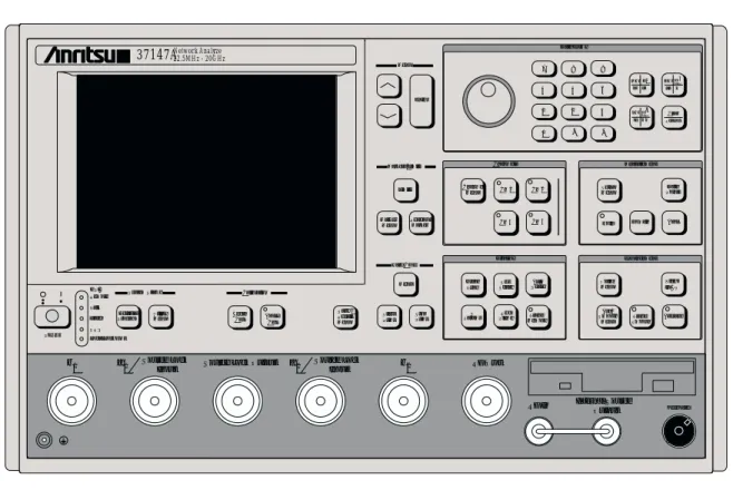
SYSTEM DESCRIPTION The 371XXC Analyzers are microprocessor controlled Vector Network An-alyzers. Each is a single-instrument system that contains a built-in signal source, a test set, and an analyzer subsystem. A typical model (37169C) is shown in Figure 1-1. These analyzers are produced in two models that cover a range of from 22.5 MHz to 40 GHz. The table at left lists the fre-quencies for each model.1-6
RELATED MANUALS The 37XXXC Vector Network Analyzer Operation Manual (10410-00226)describes the front panel operation for all 37XXXC models. It also con-tains general information, specifications, and Performance Verification procedures for all models.
The 37XXXC Series Vector Network Analyzer Programming Manual (10410-00227) describes all 37XXXC GPIB commands and provides programming information for operation of the 37XXXC remotely via the IEEE-488 General Purpose Interface Bus. Included at the rear of this manual is the 37XXXC Series Vector Network Analyzer GPIB Quick Reference Guide (10410-00229).
1-7
OPTIONS The 371XXC VNA options and their respective upgrade kit part numbersthat can be installed at ANRITSU Service Centers are:
1-8
SERVICE STRATEGY This paragraph provides an overview of the 371XXC VNA servicestrat-egy and available service facilities. It also provides references to the information in various locations in this manual needed to accomplish the service functions required for the 371XXC VNA.
Appendices - Refer to the Appendices at the rear of this manual for de-tailed descriptions of the following:
q Diagnostic Menus q GPIB Commands q Error Messages
Option Description Upgrade Kit
1 Rack Mount w/slides ND39486
1A Rack Mount ND40916
2A Time Domain (Microwave Units) ND39477 10A High Stability Ovenized Time
Base, 1 Hz Frequency Resolution
ND45045
INFORMATION
STRATEGY
Model Freq Range
37147C 22.5 MHz to 20.0 GHz
37169C 22.5 MHz to 40.0 GHz
Functional Assembly Level Troubleshooting
The 371XXC modular design, extensive built-in diagnostics, and auto-mated service tools are designed to support fast exchange of functional assembly level repairs.
Failed assemblies are not field repairable. Once an assembly is found to be faulty, it should be returned to an authorized ANRITSU Service Center for exchange. Refer to the description of the Exchange Assem-bly Program in Chapter 2, Replaceable Parts.
The procedures for troubleshooting a failed 371XXC VNA are de-scribed in this manual in Chapter 5, Troubleshooting.
Internal Hardware Adjustments and Calibrations
There are five automated internal hardware field calibrations. Two of them are used to characterize the 371XXC frequency and power genera-tion sub-systems. These calibragenera-tions insure fast, consistent phase lock of system frequencies and proper compensation, leveling, and flatness of system power at the front panel test ports.
To conduct these calibrations, you need only connect the appropriate test equipment (counter or power meter) to the 371XXC and initiate the calibration. The 371XXC will control itself and the externally con-nected test equipment to perform measurements and store calibration constants in its internal battery backed RAM (BBRAM).
The procedures for adjusting the 371XXC VNA are described in this manual in Chapter 6, Adjustments.
Internal Service Log The 371XXC continuously monitors itself for proper operation. Should a failure occur, it notifies the user via a failure message on the display screen. (In remote-only operation, it also sets the GPIB Status Byte, if enabled.) It also writes the error message along with some data pertinent to the failure to an internal service log stored in battery-backed memory. The service log can be checked at any time to view (without erasing) all error messages. It is capable of storing more than 30 pages of ser-vice messages and data. The 371XXC will automatically remove the oldest errors first to make room for new errors, if necessary. To check the contents of the service log, use the procedure described in Chapter 3, Operational Tests.
NOTE
A printed or disk file copy of the Service Log (with the fail-ure in question) must be made available to ANRITSU when exchanging a failed assembly, or when requesting service support. Refer to Chapter 2, Replaceable Parts, for further information.
System Test/ Certification
Quick operational checkout of the system may be accomplished by the system user or for incoming inspection purposes using the “Operational Checkout” chapter in the 371XXC Operations Manual. Those procedures
SERVICE
GENERAL
are useful in quickly verifying that the instrument’s primary measure-ment functions are operational and stable.
Full operational testing of the system is detailed in Chapter 3, Opera-tional Tests. These tests should be performed annually, or more often depending on system use.
Verification of the system’s measurement accuracy and other key per-formance parameters may be done using the procedures in Chapter 4, Performance Verification. This should be performed annually, or more often depending on system use.
Preventive Service The 371XXC A9 Processor PCB contains a battery-backed memory/real time clock chip (BBRAM) and a static memory (SRAM) backup battery. These have a finite life span and should be replaced periodically per the procedures in Chapter 8, Removal and Replacement Procedures. The BBRAM chip has a rated life span of four years. The SRAM backup battery has a worst case elapsed time for SRAM battery pro-tection of 200 days. The SRAM battery life span will vary according to how the system is used; that is, how often the system is powered off for extended periods of time.
Servicing Specially Modified Instruments
Instruments with customer requested special modifications performed by ANRITSU will have an identifying Specials Modification number printed on the rear panel. This number will be preceded with the letters SM, i. e., SM1234 is special modification number 1234.
Special instruments may have service requirements different from those specified in this manual. SM5235 and SM5392 are instruments designed for use with the 37100C VNA. Refer to Appendix F for ser-vice instructions. Contact your local Serser-vice Center if you need more information when servicing such instruments.
1-9
SERVICE SUPPORTINFORMATION
The following paragraphs briefly describe the various service support ser-vices and aids available to you to help you maintain your 371XXC.
Technical Support Technical service support is available by contacting any ANRITSU Worldwide Service Center (see Chapter 2).
If servicing or repairing your own system and you need technical sup-port, you will need to provide the items listed below to the ANRITSU Customer Support Engineer:
q Measurement data in question q “Operational Tests” results
q System state (from UTILITY menu) q Service Log (from DIAGNOSTICS menu)
Service Software The service software listed below is contained on the diskette located at the rear of this manual:
ANRITSU 37XXX Test Software (2300-178)
This software contains a series of automated tests designed to insure the 371XXC signal paths are functioning properly and capable of sup-porting stable calibrations and measurements. See Operational Tests Chapter for details.
Test Fixtures/ Aids The test fixtures and test aids listed below are available through your lo-cal ANRITSU Sales or Service Center:
Rear Panel Printer Port Test Fixture (B39553)
This test fixture is used to check out digital printer interface circuits on the rear panel assembly.
GPIB Cable (2100-2)
This cable is used to check out digital GPIB interface circuits on the rear panel assembly.
Front Panel Source Lock Test Fixture (ND45331)
This test fixture is used to evaluate system performance.
Front Panel Test Signal Lock Test Fixture (ND45332)
This test fixture is used to evaluate system performance.
Failed Assembly Exchange Program
The exchange program allows a customer to quickly exchange a failed subassembly for a factory refurbished, fully system-tested end unit that is under warranty. This results in significant time and price savings as com-pared with ordering a new assembly.
Refer to Chapter 2, Replaceable Parts, for a complete list of exchange-able assemblies for all Series 37100C models.
NOTE
When sending a failed assembly to the factory for ex-change, a copy of the Service Log must always accom-pany the failed assembly. Refer to Chapter 2, Replaceable Parts, for further information.
SERVICE SUPPORT
GENERAL
1-10
RECOMMENDED TEST EQUIPMENTTable 1-1 lists the recommended test equipment to be used for all mainte-nance activities for all Series 37100C models. Note the “Use” codes listed in the right hand column of the table. These codes list the appli-cable maintenance activities for the equipment listed.
INSTRUMENT CRITICAL
SPECIFICATION
RECOMMENDED
MANUFACTURER/MODEL USE**
Computer/Controller Equipped with National Instruments
GPIB Interface Adapter, w/Driver Soft-ware and Windows 95/98
Any O, P
Test Software ANRITSU 2300-178 O
Floppy Disk Formatted, IBM PC format DS/HD 1.44 Mbyte A
GPIB Cable ANRITSU 2100-2, or equivalent O, P, A
RF/Microwave Cable DC – 40 GHz, K type connectors (male
or female), Length, 3 ft.
Any P, A
BNC Cable Length, 4 ft., 2 each Any O
Printer Port Test Fixture ANRITSU B39553 O
Front Panel Source Lock Test Fixture ANRITSU ND45331 O, P
Front Panel Test Signal Test Fixture ANRITSU ND45332 O, P
Fixed Attenuator Contains test data ANRITSU 41KC-10, w/Opt C P
Fixed Attenuator ANRITSU 41KC-3 P
Thru Line ANRITSU 3670K50-2, 3671K50-2 O
Calibration Kit ANRITSU 3652 O, P
Frequency Counter Frequency: 0.1 to 26.5 GHz
Input Impedance: 50W
EIP Microwave, Inc., with GPIB and Band 3 Input
P, A
Digital Multimeter Resolution: 41
2digits DC Accuracy: 0.1 % AC Accuracy: 0.1 % Any T Oscilloscope Bandwidth: DC to 100 MHz Sensitivity: 2 mV
Horiz. Sensitivity: 50 ns/division
Any T
Power Meter and Power Sensor
Anritsu Model ML243xA Power Me-ter, with MA2474A
P, A
Gauging Set GPC-7 Gauging Set
K Connector Gauging Set
ANRITSU 01-161 ANRITSU 01-162
O, T
** USE CODES:
A Adjustment / Internal Hardware Calibration
O Operational Testing
P Performance Verification
T Troubleshooting
Table 1-1. Recommended Test Equipment (1 of 1)
1-11
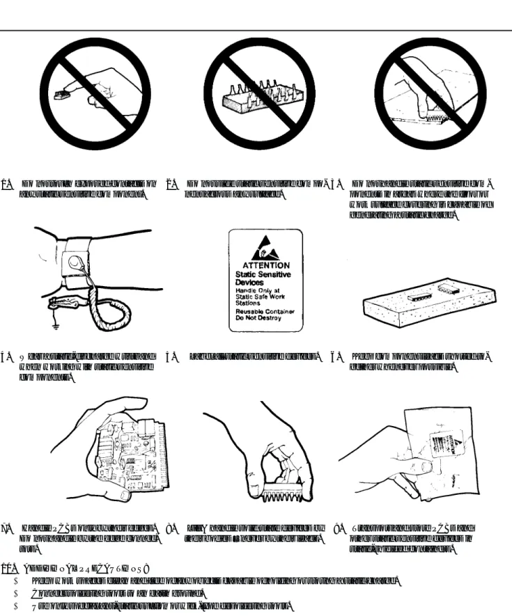
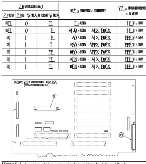
STATIC SENSITIVE COMPONENT HANDLING PROCEDURESThe 371XXC contains components that can be damaged by static electric-ity. Figure 1-2 (next page) illustrates the precautions that should be fol-lowed when handling static-sensitive subassemblies and components. If followed, these precautions will minimize the possibilities of static-shock damage to these items.
1-12
SERVICE CENTERS ANRITSU Company offers a full range of repair and calibration services at fully staffed and equipped service centers throughout the world. Table 2-1, located on page 2-4, lists all ANRITSU service centers.1-13
PERFORMANCESPECIFICATIONS
The performance specifications for all Series 371XXC models are con-tained in the Technical Data Sheet that is located in Appendix D, Per-formance Specifications.
GENERAL
SERVICE
1. Do not touch exposed contacts on any static sensitive component.
2. Do not slide static sensitive compo-nent across any surface.
3. Do not handle static sensitive com-ponents in areas where the floor or work surface covering is capable of generating a static charge.
4. Wear a static-discharge wristband when working with static sensitive components.
5. Label all static sensitive devices. 6. Keep component leads shorted to-gether whenever possible.
7. Handle PCBs only by their edges. Do not handle by the edge connec-tors.
8. Lift & handle solid state devices by their bodies – never by their leads.
9. Transport and store PCBs and other static sensitive devices in static-shielded containers.
10. ADDITIONAL PRECAUTIONS:
· Keep work spaces clean and free of any objects capable of holding or storing a static charge. · Connect soldering tools to an earth ground.
· Use only special anti-static suction or wick-type desoldering tools.
Figure 1-2. Static Sensitive Component Handling Procedures
Table of Contents
2-1 INTRODUCTION · · · 2-3 2-2 EXCHANGE ASSEMBLY PROGRAM · · · 2-3 2-3 REPLACEABLE SUBASSEMBLIES AND PARTS · · · 2-3 2-4 PARTS ORDERING INFORMATION · · · 2-4
Chapter 2
Chapter 2
Replaceable Parts
2-1
INTRODUCTION This chapter provides replaceable parts information for all 371XXCmodels. The major replaceable 371XXC assemblies and parts are listed in Tables 2-2 through 2-7. The locations of these assem-blies/parts are shown in Figures 2-1 through 2-3.
2-2
EXCHANGE ASSEMBLYPROGRAM
ANRITSU maintains a module exchange program for selected subassem-blies. If a malfunction occurs in one of these subassemblies, the defective item can be exchanged. Upon receiving your request, ANRITSU will ship the exchange subassembly to you, typically within 24 hours. You then have 45 days in which to return the defective item. All exchange subas-semblies or RF assubas-semblies are warranted for 90 days from the date of shipment, or for the balance of the original equipment warranty, which-ever is longer.
NOTE
When sending a failed assembly to the factory for ex-change, a copy of the Service Log must always accom-pany the failed assembly. This copy may be a printout, or a saved disk copy. Due to the importance of the service log information to the ANRITSU factory Service Engineers, the exchange prices are only valid if the service log data is included with the failed assembly.
Please have the exact model number and serial number of your unit available when requesting this service, as the information about your unit is filed according to the instrument's model and serial number. For more information about the program, contact your local sales rep-resentative or call ANRITSU Customer Service direct (refer to para-graph 2-4.
2-3
REPLACEABLESUBASSEMBLIES AND PARTS
Tables 2-2 through 2-5, (starting page 2-5) list the major replaceable sub-assemblies and parts for the 371XXC. These sub-assemblies/parts are pres-ently covered by the ANRITSU exchange assembly program. Table 2-6 (page 2-6) lists disposable parts for the 371XXC, and Table 2-7 lists fac-tory-repairable parts for the 371XXC. (The parts listed in Tables 2-6 and 2-7 are not presently on the exchange assembly program.)
NOTE
The 371XXC A17 Motherboard PCB Assembly is not a field-replaceable item.
2-4
PARTS ORDERING INFORMATIONAll parts listed in Tables 2-2 through 2-7 may be ordered from your local ANRITSU service center (Table 2-1).
REPLACEABLE
PARTS ORDERING
PARTS
INFORMATION
UNITED STATES ANRITSU COMPANY 490 Jarvis Drive Morgan Hill, CA 95037-2809 Telephone: (408) 776-8300 1-800-ANRITSU FAX: 408-776-1744 FRANCE ANRITSU S.A 9 Avenue du Quebec Zone de Courtaboeuf 91951 Les Ulis Cedex Telephone: 016-09-21-550 FAX: 016-44-61-065JAPAN
ANRITSU CUSTOMER SERVICE LTD. 1800 Onna Atsugi-shi
Kanagawa-Prf. 243 Japan Telephone: 0462-96-6688 FAX: 0462-25-8379
ANRITSU COMPANY 10 New Maple Ave., Unit 305 Pine Brook, NJ 07058 Telephone: (973) 227-8999 1-800-ANRITSU FAX: 973-575-0092 GERMANY ANRITSU GmbH Grafenberger Allee 54-56 D-40237 Dusseldorf, Germany Telephone: 0211-968550 FAX: 0211-9685555 SINGAPORE
ANRITSU (SINGAPORE) PTE LTD. 10, Hoe Chiang Road
#07-01/02 Keppel Towers Singapore 089315 Telephone: 282-2400 FAX: 282-2533 ANRITSU COMPANY 1155 E. Collins Blvd Richardson, TX 75081 Telephone: 1-800-ANRITSU FAX: 972-671-1877 INDIA MEERA AGENCIES PVT. LTD. 23 Community Centre
Zamrudpur, Kailash Colony Extension, New Delhi, India 110 048
Phone: 011-6442700/6442800 FAX : 011-644250023
SOUTH AFRICA
ETECSA
12 Surrey Square Office Park 330 Surrey Avenue Ferndale, Randburt, 2194 South Africa Telephone: 011-27-11-787-7200 FAX: 011-27-11-787-0446 AUSTRALIA ANRITSU PTY. LTD. Unit 3, 170 Foster Road Mt Waverley, VIC 3149 Australia Telephone: 03-9558-8177 FAX: 03-9558-8255 ISRAEL TECH-CENT, LTD. 4 Raul Valenberg St Tel-Aviv 69719 Telephone: (03) 64-78-563 FAX: (03) 64-78-334 SWEDEN ANRITSU AB Botivid Center Fittja Backe 13A 145 84 Stockholmn Telephone: (08) 534-707-00 FAX: (08) 534-707-30
BRAZIL
ANRITSU ELECTRONICA LTDA. Praia de Botafogo, 440, Sala 2401 CEP22250-040, Rio de Janeiro, RJ, Brasil Telephone: 021-527-6922 FAX: 021-53-71-456 ITALY ANRITSU Sp.A Roma Office Via E. Vittorini, 129 00144 Roma EUR Telephone: (06) 50-99-711 FAX: (06) 50-22-4252 TAIWAN ANRITSU CO., LTD. 6F, No. 96, Section 3 Chien Kuo N. Road Taipei, Taiwan, R.O.C. Telephone: (02) 515-6050 FAX: (02) 509-5519
CANADA
ANRITSU INSTRUMENTS LTD. 700 Silver Seven Road, Suite 120 Kanata, Ontario K2V 1C3 Telephone: (613) 591-2003 FAX: (613) 591-1006 KOREA ANRITSU CORPORATION LTD. Head Office: 14F, Hyunjuk Building 832-41 Yeoksam-Dong, Kangnam-Ku Seoul 135-080, South Korea Telephone: 02-553-6603 FAX: 02-553-6604 Service Center: 8F Samwon Building 1329-8, Seocho-Dong Seocho-Ku
Seoul, South Korea 137-070 Telephone: 02-581-6603 FAX: 02-582-6603 UNITED KINGDOM ANRITSU LTD. 200 Capability Green Luton, Bedfordshire LU1 3LU, England Telephone: 015-82-433200 FAX: 015-82-731303
CHINA
ANRITSU ELECTRONICS (SHANGHAI) CO. LTD.
2F, Rm B, 52 Section Factory Building No. 516 Fu Te Rd (N)
Shanghai 200131 P.R. China Telephone:21-58680226, 58680227, 58680228
FAX: 21-58680588
Reference Designator
371XXC
Option Assembly / Part Part Number
A1 LO1 D46866-7 A2 LO2 50725-3 A3 Test A IF D38503-4 A4 Reference IF D41794-4 A5* A/D D38505-3 A6 Test B IF D38503-5
A7 without Opt 10A LO3 D38507-3
A7 with Opt 10A LO3 D38507-4
A8 Source Lock/ Separation Control 49334-4
A9 Main Processor ND55009
A13 I/O #1 D38513-3
A14 I/O #2 D38514-3
A15 Graphics Processor D44281-3
A16 Hard Disk (w/ PCB) ND55506
A18 Rear Panel PCB D44255-3
A19 Front Panel Switch PCB D44279-3
A20** Front Panel Control PCB D44280-3
A21A1 Source YIG/Bias Control (p/o Signal Source Module) 48512-3
A21A2 Source Control (p/o Signal Source Module) 48513-3
A24 VME Bus Terminator D38524-3
* NOTE: When the A5 PCB is replaced, all switches on the new PCB must be changed to match the settings found on the previous PCB.
Table 2-2. Printed Circuit Board Assemblies
Assembly / Part 371XXC Model / Option Part Number
Level Detector All C24950-2
40 GHz Quad Buffer Power Amp All see Table 2-7
Switched Doubler Module (SDM) 37169C only D28540
RF Splitter All K241C
Table 2-3. Test Set Assembly RF/Microwave Components
Assembly / Part 371XXC Model / Option Part Number
YIG Oscillator (2 - 20 GHz) All C21620-1
Down Converter All D27532
Switched Filter All D45243
Table 2-4. Signal Source Module RF/Microwave Components
Assembly / Part 371XXC Model / Option Part Number
10 MHz Ovenized Oscillator Option 10A only ND39476
Power Supply Module All 54908
LCD Display All 15-100
Floppy Disk Assy All C38550
Fan Assembly, Rear Panel All B38533
Front Panel RF Connector All B15660
Table 2-5. Miscellaneous /Integrated Assemblies
Assembly / Part 371XXC Model / Option Part Number
System Software All 2300-212
Front Panel Encoder Knob All 2000-557
Fuse, 8A, Fast Blow 3AG Cartridge type (F1 Line fuse for power supply assembly)
All 631-72
Battery Backed RAM All 54-1350
Back-Up Battery All 633-20*
* 54347 PCB only
Table 2-6. Consumable Parts
REPLACEABLE
PARTS
PARTS
LISTS
Buffer Amp Label Replacement Buffer/Power Amp Kit
D44364 ND54995
ND54966 ND54995
54277 ND54988
58437 ND54988
Signal Source Module Power Supply Module Ovenized Reference Oscillator
(Option 10A only)
Printed Circuit Boa Assemblies, A1-A Fan Assembly
Printed Circuit Board Assemblies,
A13-A16
Figure 2-1. 371XXC Major Assemblies Location Diagram (Top3 4View)
Floppy Disk Drive Assembly
A17 Motherboard PCB Assembly
A24 VME Bus Terminator PCB Assembly
Model 37169C Only
* A18 Rear PanelPCB Assembly
Buffer/Power Amplifier Switched Doubler Module* RF Splitter Level Detector
Figure 2-2. 371XXC Major Assemblies Location Diagram (Bottom View)
REPLACEABLE
PARTS
Figure 2-3. Signal Source Parts Location Diagram
Table of Contents
3-1 INTRODUCTION · · · 3-3 3-2 CHECKING THE SERVICE LOG · · · 3-4 3-3 SELF TEST · · · 3-5 3-4 PERIPHERALS AND INTERFACES TESTS · · · 3-6 Display Test· · · 3-6 Front Panel Test · · · 3-7 External Keyboard Interface Test · · · 3-7 Printer Interface Test · · · 3-7 GPIB Interface Test · · · 3-9
Chapter 3
Chapter 3
Operational Tests
3-1
INTRODUCTION The tests in this section provide a means of fully testing the 371XXCVNA system for proper operation and signal stability. These tests are in-tended to be used as a periodic check of the operational functionality of the 371XXC.
The tests should be performed in their entirety at least once annually. Although there is no requirement to do so, the tests should generally be run in the sequence presented.
NOTE
The procedures presented in Chapter 4, Performance Veri-fication, provide the means to test the accuracy of the tests performed by the 371XXC.
Please ensure you have read and fully understand the servicing con-cepts for the 371XXC presented in Chapter 1 prior to continuing with this chapter.
Operational Tests for the 371XXC consist of the following: q Checking the Service Log
q Self Test
q Peripherals and Interface Testing
q Signal Path Tests (includes Checking the Service Log and Self Test.)
These tests are described in paragraphs 3-2 through 3-5, which start on the next page.
3-2
CHECKING THE SERVICE LOGChecking the service log consists of viewing the entries written into the log.
CAUTION
The service log contains historical information about in-strument condition and any failures that may have oc-curred. It should be cleared only by a qualified service engineer. Such clearing should be accomplished only upon determining that the errors need not be saved to disk, or printed out for service purposes.
Procedure:
Step 1. Press theOption Menukey (Enhancement key group) to display the OPTIONS menu.
Step 2. Select DIAGNOSTICS from the OPTIONS menu (left); then select READ SERVICE LOG from the DIAGNOS-TICS menu.
The 371XXC will now display the contents of the service log. The display consists of a header and an error listing. The header contains a variety of system service informa-tion. The error listing contains error messages for failures that may have occurred during operation.
NOTE
· Errors 7201–7209, GPIB remote opera-tion programming errors, report that one or more external GPIB programming er-rors has been detected. These messages do not indicate a 371XXC system fault.
· Informational messages 0000–0099 report the pass/fail status of a peripheral access. These messages do not indicate a 371XXC system fault.
Any other error messages in the service log may indicate an instrument problem and should be investigated. Refer to the Chapter 5, Troubleshooting, for further information.
CAUTION
The CLEAR SERVICE LOG menu selec-tion will immediately and permanently clear all the error message entries from the serv-ice log. (However, it will not clear the header information.) See Caution message at top of page.
OPERATIONAL
CHECKING THE
TESTS
SERVICE LOG
OPTIONS TRIGGERS REAR PANEL OUTPUT DIAGNOSTICS MULTIPLE SOURCE CONTROL PRESS <ENTER> TO SELECT DIAGNOSTICS
START SELF TEST
READ SERVICE LOG
INSTALLED OPTIONS PERIPHERAL TESTS TROUBLESHOOTING (FOR SERVICE ONLY) HW CALIBRATIONS (FOR SERVICE ONLY) PRESS <ENTER> TO SELECT
3-3
SELF TEST The self test performs a series of tests that verify that various internal 371XXC circuits are functional and operating properly. Note that system must be free of Lock Failure error messages to perform the self-test.To start the self test:
Step 1. Press theOption Menukey (Enhancement key group) to display the OPTIONS menu.
Step 2. Select DIAGNOSTICS from the OPTIONS menu; then se-lect START SELF TEST (below).
Step 3. Wait for test sequence to complete. (Once invoked, this test requires no user interaction or external equipment.) Upon completion, the net pass/fail result of the self test is shown on the display. If the 371XXC is in remote-only operation, the results are reported via the GPIB output buffer. If the self test fails, detailed error messages will be written into the service log.
If self test fails:
qCheck the service log to view failure messages.
qProceed to Chapter 5, Troubleshooting.
TEST
TESTS
OPTIONS TRIGGERS REAR PANEL OUTPUT DIAGNOSTICS MULTIPLE SOURCE CONTROL PRESS <ENTER> TO SELECT DIAGNOSTICS START SELF TESTREAD SERVICE LOG INSTALLED OPTIONS PERIPHERAL TESTS TROUBLESHOOTING (FOR SERVICE ONLY) HW CALIBRATIONS (FOR SERVICE ONLY) PRESS <ENTER> TO SELECT
3-4
PERIPHERALS AND INTERFACES TESTSThese tests are used to verify the operation of the LCD display, front panel keys, and peripheral devices that are used with the 371XXC. They consist of the following:
q LCD Display Test q Front Panel Test
q External Keyboard Interface Test q Printer Interface Test
q GPIB Interface Test
Display Test This test verifies that the 371XXC display is functioning correctly.
NOTE
The External VGA Out Connector can also be tested when using this procedure if an external VGA monitor is con-nected.
Procedure:
Step 1. Press theOption Menukey (Enhancement key group) to display the OPTIONS menu.
Step 2. Select DIAGNOSTICS from menu; then in sequence se-lect: PERIPHERAL TESTS, and then CRT DISPLAY. See diagram below.
Step 3. Follow instructions on the LCD until test is completed. If test fails, proceed to Chapter 5, Troubleshooting.
OPERATIONAL
PERIPHERALS AND
TESTS
INTERFACES TESTS
OPTIONS TRIGGERS REAR PANEL OUTPUT DIAGNOSTICS MULTIPLE SOURCE CONTROL PRESS <ENTER> TO SELECT DIAGNOSTICS
START SELF TEST READ SERVICE LOG INSTALLED OPTIONS PERIPHERAL TESTS TROUBLESHOOTING (FOR SERVICE ONLY) HW CALIBRATIONS (FOR SERVICE ONLY) PRESS <ENTER> TO SELECT PERIPHERAL TESTS CRT DISPLAY FRONT PANEL EXTERNAL KEY-BOARD PRINTER INTERFACE GPIB INTERFACE PREVIOUS MENU PRESS <ENTER> TO SELECT
Front Panel Test This test verifies that the control keys in each of the 371XXC key groups are functioning correctly.
Procedure:
Step 1. Press theOption Menukey (Enhancement key group) to display the OPTIONS menu.
Step 2. Select DIAGNOSTICS from the OPTIONS menu; then in sequence select: PERIPHERAL TESTS, and then
FRONT PANEL. See diagram below.
Step 3. Follow instructions on the screen until test is completed. If test fails, proceed to Chapter 5, Troubleshooting.
External Keyboard Interface Test
This test verifies that the 371XXC external keyboard interface is func-tioning correctly.
Equipment Required:
An IBM compatible keyboard is required for this test.
Procedure:
Step 1. Press theOption Menukey (Enhancement key group) to display the OPTIONS menu.
Step 2. Select DIAGNOSTICS from the OPTIONS menu; then in sequence select: PERIPHERAL TESTS, and then
EX-TERNAL KEYBOARD. See diagram above.
Step 3. Follow instructions on the screen until test is completed. If test fails, proceed to Chapter 5, Troubleshooting.
Printer Interface Test This test verifies that the 371XXC printer interface is functioning cor-rectly.
INTERFACES TESTS
TESTS
OPTIONS TRIGGERS REAR PANEL OUTPUT DIAGNOSTICS MULTIPLE SOURCE CONTROL PRESS <ENTER> TO SELECT DIAGNOSTICS
START SELF TEST READ SERVICE LOG INSTALLED OPTIONS PERIPHERAL TESTS TROUBLESHOOTING (FOR SERVICE ONLY) HW CALIBRATIONS (FOR SERVICE ONLY) PRESS <ENTER> TO SELECT PERIPHERAL TESTS CRT DISPLAY FRONT PANEL EXTERNAL KEY-BOARD PRINTER INTERFACE GPIB INTERFACE PREVIOUS MENU PRESS <ENTER> TO SELECT
Equipment Required:
Printer Test Fixture (ANRITSU PN: B39553)
Procedure:
Step 1. Press theOption Menukey (Enhancement key group) to display the OPTIONS menu.
Step 2. Select DIAGNOSTICS from menu; then in sequence se-lect: PERIPHERAL TESTS, and then PRINTER
INTERFACE. See diagram below.
Step 3. Follow instructions on the screen until test is completed. If test fails, proceed to Chapter 5, Troubleshooting.
OPTIONS TRIGGERS REAR PANEL OUTPUT DIAGNOSTICS MULTIPLE SOURCE CONTROL PRESS <ENTER> TO SELECT DIAGNOSTICS
START SELF TEST READ SERVICE LOG INSTALLED OPTIONS PERIPHERAL TESTS TROUBLESHOOTING (FOR SERVICE ONLY) HW CALIBRATIONS (FOR SERVICE ONLY) PRESS <ENTER> TO SELECT PERIPHERAL TESTS CRT DISPLAY FRONT PANEL EXTERNAL KEY-BOARD PRINTER INTERFACE GPIB INTERFACE PREVIOUS MENU PRESS <ENTER> TO SELECT
OPERATIONAL
PERIPHERALS AND
GPIB Interface Test This test verifies that the 371XXC printer interface is functioning cor-rectly.
Equipment Required:
GPIB cable (ANRITSU PN: 2100-2), or equivalent
CAUTION
Insure that no other cables are connected to either of the two rear panel GPIB ports when performing this test.
Procedure:
Step 1. Press theOption Menukey (Enhancement key group) to display the OPTIONS menu.
Step 2. Select DIAGNOSTICS from menu; then in sequence se-lect: PERIPHERAL TESTS, and then GPIB
INTER-FACE. See diagram below.
Step 3. Follow instructions on the screen until test is completed. If test fails, proceed to Chapter 5, Troubleshooting.
OPTIONS TRIGGERS REAR PANEL OUTPUT DIAGNOSTICS MULTIPLE SOURCE CONTROL PRESS <ENTER> TO SELECT DIAGNOSTICS
START SELF TEST READ SERVICE LOG INSTALLED OPTIONS PERIPHERAL TESTS TROUBLESHOOTING (FOR SERVICE ONLY) HW CALIBRATIONS (FOR SERVICE ONLY) PRESS <ENTER> TO SELECT PERIPHERAL TESTS CRT DISPLAY FRONT PANEL EXTERNAL KEY-BOARD PRINTER INTERFACE GPIB INTERFACE PREVIOUS MENU PRESS <ENTER> TO SELECT
Table of Contents
4-1 INTRODUCTION · · · 4-3 4-2 CALIBRATION AND MEASUREMENT CONDITIONS · · · · 4-3 Standard Conditions · · · 4-3 Special Precautions· · · 4-4 4-3 PERFORMANCE VERIFICATION PROCEDURE · · · 4-4 Noise Floor/Receiver Dynamic Range Test · · · 4-5 Compression Test for 37147C, 37169C · · · 4-9
Chapter 4
Chapter 4
Performance Verification
4-1
INTRODUCTION This chapter provides specific procedures to be used to verify that the371XXC is making accurate, traceable S-parameter measurements. You should perform the verification procedures in paragraph 4-3, “Verifying Measurement Accuracy,” at least once annually. Much of the performance verification procedure is fully contained in the 2300-178 (3700Test.exe) program. This program also verifies the performance of the SM5392 and SM5235.
Additionally, this chapter includes procedures that may be used to measure the following key system performance parameters:
q Compression Level
q Noise Floor/Receiver Dynamic Range
Please ensure you have read and fully understand the servicing con-cepts for the 371XXC presented in Chapter 1 prior to continuing with this chapter.
4-2
CALIBRATION ANDMEASUREMENT CONDITIONS
Extremes in the surrounding environmental conditions and the condition and stability of the test port connectors, through-cable, and calibration kit determine system measurement integrity to a large extent.
These are all user controlled conditions, and as such, should be evalu-ated periodically for impact on system performance. If these conditions vary significantly with time, the system verification procedures should be performed more often than the recommended annual cycle.
Standard Conditions The standard conditions specified below must be observed when perform-ing any of the operations in this chapter—both durperform-ing calibration and during measurement.
Warm-up Time: One hour minimum. Environmental Conditions:
Temperature: 23 +/- 3 deg C
Special Precautions When performing the procedures in this chapter, observe the following precautions:
q Minimize vibration and movement of system and attached compo-nents and through-cable.
q Clean and check pin depth and condition of all adapters, through-cable(s), and calibration components.
q Pre-shape the through-cable(s) so as to minimize its movement dur-ing calibration and measurement activities.
q Ensure the system remains motion free in stable environmental conditions as defined above throughout warm-up, calibration, and measurement activities.
4-3
PERFORMANCEVERIFICATION PROCEDURE
The following are the specific tests that should be used to verify the per-formance of the 371XXC. Equipment required for these tests is shown be-low.
Qty Item
1 Computer/Controller as described in Table 1-1
1 ANRITSU 3652 Calibration Kit
1 EIP 548 Frequency Counter, with GPIB and Band 3 input
1 ANRITSU ML243XA
1 ANRITSU MA2474A
1 ANRITSU ND45331 Test Fixture Kit
1 ANRITSU ND45332 Test Fixture Kit
1 ANRITSU 3670K50-1 Through Cable
1 ANRITSU 3670K50-2 Through Cable
1 ANRITSU 41KC-10 with Option C
2 ANRITSU 43KC-3
1 ANRITSU 33KFKF50 Insertable
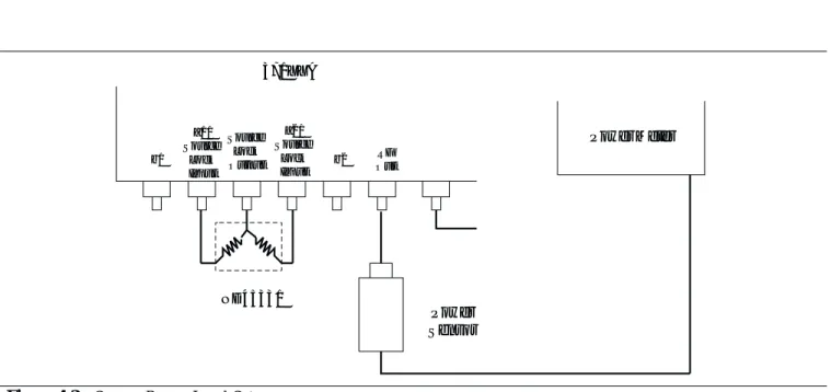
Step 1. Connect Test Fixtures ND45331 and ND45332 to the 371XXC as shown in Figure 4-1 on the next page.
Step 2. Launch the 2300-178 program (3700Test.exe).
Step 3. Follow the instructions displayed by program. If problems occur at startup, refer to the *.doc file on the disk.
Step 4. Run all tests that are displayed. To launch a test, click on the label. All specifications and instructions are within the software. Pass/fail results and test data are saved in the host computer’s C:\37000 folder.
PERFORMANCE VERIFICATION
PERFORMANCE
Noise Floor/Receiver Dynamic Range Test
Noise Floor is the small signal response resulting from noise. It estab-lishes the lowest level of signal detection. The Receiver Dynamic Range is the difference between the receiver compression level and the noise floor. This test verifies that the noise floor meets the guaranteed performance specifications.
Test Procedure Part A, Set Source Power Level
The following test uses a Power Meter to calibrate the Source output power setting at specified frequency points across the Frequency cov-erage range of the 371XXC.
Step 1. Set up the equipment per Figure 4-2. Do not connect the Power Sensor toRF Outat this time.
Step 2. Zero and calibrate the Power Sensor, then connect it toRF Out.
Step 3. Press theSetup Menukey and select TEST SIGNALS.
Step 4. Move the cursor to C.W. MODE and press theEnterkey.
b1 371XXA Source Lock Output a1/ Source Lock Input a2/ Source Lock Input b2 OutRF 43KC-3 43KC-3 43KC-10 K241C K241C
Figure 4-1. Connecting the Test Fixtures
Step 5. Set C.W. Frequency for the first frequency listed below; 22.5 MHz if this is the first time through this step. Set C.W. Frequency for 2 GHz for the second time through, 20 GHz for the third time, and so on.
Step 6. Adjust the source power control so that the power meter displays the power shown in the Rated Power Level column in the table above. Use the attenuator if necessary and set the appropriate Cal Factor on the power meter as required for each frequency.
Step 7. Record the Source Power Control setting that gives the Rated Power in the last column of the table above.
Step 8. Repeat Steps 5 through 7 for the rest of the frequencies listed in Step 5, above.
Power Meter 371XXA Source Lock Output a1/ Source Lock Input a2/ Source Lock Input RF Out b1 b2 Power Sensor ND45331
Figure 4-2. Source Power Level Setup
Frequency (GHz)
Rated Power Level (dBm)
Source Power Control Setting to Achieve Rated
Power Level (dB)
0.0225 -18
2.0 -12
20.0 -12
40.0 -15
Table 4-1. Source Power Control Settings
PERFORMANCE VERIFICATION
PERFORMANCE
Test Procedure Part B, Noise Floor/Receiver Dynamic Range
The following test verifies the Receiver Dynamic Range and Noise Floor performance.
Step 1. Set up the equipment per Figure 4-3.
Step 2. Set the 371XXC as shown below.
Key Menu Choice
CHANNEL MENU SINGLE CHANNEL
S-PARAMS S21 (Channel 1)
Step 3. Press theBegin Calkey.
Step 4. Select from the displayed prompts to perform a C.W. (1 POINT), STANDARD, COAXIAL, or TRANSMISSION FREQUENCY RESPONSE (S21) Calibration for the first frequency listed in Table 4-1, previous page. Set C.W. Fre-quency for 22.5 MHz if this is the first time through this step. Set C.W. Frequency for 2 GHz for the second time through, 20 GHz for the third time and so on. Note: When prompted for isolation devices, connect terminations tob2
andRF Out.
Step 5. When the CONFIRM CALIBRATION PARAMETERS menu appears, select TEST SIGNALS.
Step 6. Set the POWER CONTROL selection to the power level re-corded in Table 4-1 for the applicable frequency, then select RESUME CAL.
Step 7. Follow the displayed prompts to complete the calibration. b1 371XXA Source Lock Output a1/ Source Lock Input a2/ Source Lock Input b2 OutRF ND45331
Figure 4-3. Noise Floor/Receiver Dynamic Range Setup
Step 8. Disconnect the cable fromb2andRF Outand connect 50 ohm terminations tob2andRF Out.
Step 9. Set up the 371XXC as shown.
Key Menu Choice
GRAPH TYPE LOG MAGNITUDE
SET SCALE RESOLUTION: 20 dB/DIV, REF VALUE:
–80 dB
DATA POINT POINT DRAWN IN C.W. 20
AVG/SMOOTH MENU AVERAGING: 512 MEAS. PER POINT
AVERAGE ON
VIDEO IF BW MINIMUM
Step 10. Press theTrace Memorykey.
Step 11. Select VIEW DATA and wait one complete sweep, then se-lect STORE DATA TO MEMORY.
Step 12. Select VIEW DATA (-) MEMORY. Note: Use the SELECT TRACE MATH menu option to change to VIEW DATA (-) MEMORY.
Step 13. Allow one full sweep to occur, then press theHoldkey.
Step 14. Press theMarker Menukey and enable MARKER 1.
Step 15. PressReadout Markerkey, select MARKER TO MAX and record the value in the “Dynamic Range” column below.
Frequency (GHz) Dynamic Range (dB) Specification
0.0225 104
2 94
20 91
40 85
Step 16. Repeat Steps 3 through 15 for the rest of applicable fre-quencies listed in Step 15, above.
PERFORMANCE VERIFICATION
PERFORMANCE
Step 17. Compute the Noise Floor for each frequency and record it in the table below. The formula is:
Noise Floor (dBm) =
Rated Power (from Table 4-1 on page 4-6) - Dynamic Range Example: For 22.5 MHz, max. PWR Level for 0.1 dB Compression is –12 dBm.
Frequency (GHz) Noise Floor (dBm) Specification
0.0225 –122
2 –106
20 –103
40 –100
Compression Test for 37147C, 37169C
Proceed as follows:
Preliminary
Step 1. Install the ND45331 to the Source Lock Output connector as shown on Figure 4-1.
Model 37147C Setup:
Step 1. Remove the 10dB attenuator from the input of the ND45332, and install a model 43KC-6 in that position.
Step 2. Install the ND45332 to the RF OUT and the B1 and B2 connectors of the 37147C (Figure 4-1).
Model 37169C Setup:
Step 1. Remove all three 43KC-X pads from the ND45332 fixture, and install the fixture to RF OUT, B1 and B2 connectors of the 37169C (Figure 4-1).
Step 2. For Both Models: PressDEFAULT PROGRAM key two times.
Step 3. Set the instrument as shown in the following chart:
Key Menu Choice
SETUP MENU Start 22.5 MHz; Stop 270 MHz
37147C: Test Signals/ Power Control -18dB 37169C: Test Signals/Power Control -16 dB
CHANNEL MENU Dual Channels, 1 & 3
GRAPH TYPE LOG MAGNITUDE, both channels
S-PARAMS Ch1 = S12
SET SCALE RESOLUTION: 0.1 dB per Division (both
channels)
REFERENCE VALUE: 0 dB
LIMITS: Upper Limit ON; set to +0.1 dB (both channels)
Lower Limit On, set to -0.1 dB, both channels
Step 4. Normalize Channel 1 by pressing the TRACE MEMORY key.
Step 5. Allow a few sweeps to occur.
Step 6. Select “Store Data to Memory”, then “View Data/Memory”.
Step 7. Repeat for Channel 3. Data will be a flat line on the 0dB reference line.
Step 8. Increase the Power Control by 10 dB (to-8 dB on the 37147C, or-6 dB on the 37169C).
Step 9. Ensure displays fall between the Limit Lines.
Step 10. Change the Start Frequency to 271 MHz and Stop Fre-quency to 20 GHz.
Step 11. Select “View Data” under theTRACE MEMORYkey (for both channels).
Step 12. Set the Power Control as follows: 37147C:-11 dB
37169C:-13 dB
Step 13. Normalize the displays (“Store Data to Memory”, then “View Data/Memory”)
Step 14. Raise the Power Control by 10 dB (to-1 dB on the 37147C, or-3 dB on the 37169C).
Step 15. Ensure all displays fall between the Limit Lines.
PERFORMANCE VERIFICATION
PERFORMANCE
Step 16. If the VNA is a model 37147C, the test is complete. Return the ND45332 to normal by reinstalling the 43KC-10 pad (model 37147C only). If the VNA is a model 37169C, con-tinue with Step 17.
Step 17. Set the Stop Frequency to 40 GHz , and the Start to 20 GHz.
Step 18. Select “View Data.”
Step 19. Set the Power Control to-14 dB.
Step 20. Normalize the display (“Store Data to Memory”, then “View Data/Memory’).
Step 21. Increase the Power Control to-4 dB. Insure the data falls between the Limit Lines
Step 22. Return the ND45332 fixture to normal (reinstall the 43KC-x pads, insuring the 10 dB pad is on the input to the splitter).
Table of Contents
5-1 INTRODUCTION · · · 5-3 5-2 ASSOCIATED INFORMATION IN THIS MANUAL · · · 5-4 5-3 RECOMMENDED TEST EQUIPMENT · · · 5-4 5-4 IF SYSTEM DOES NOT POWER-UP · · · 5-4 Line Source and Interface Checks · · · 5-4 Power Supply Voltages Check · · · 5-4 Power Supply Module Check· · · 5-6 5-5 IF SYSTEM DOES NOT BOOT-UP· · · 5-7 Boot-up Process Sequence · · · 5-7 Troubleshooting Boot-up Problems · · · 5-8 Hard Disk Problem 1 · · · 5-8 Hard Disk Problem 2 · · · 5-9 Floppy Disk Problems · · · 5-9 Screen Display Problems· · · 5-9 5-6 IF SYSTEM PRODUCES AN ERROR CODE· · · 5-10 Phase Lock Error Codes (6000 Series) · · · 5-11 Service Log Snap Shot Data · · · 5-12 5-7 SIGNAL SOURCE, TEST SET, AND
RECEIVER PROBLEMS · · · 5-13 Signal Source Phase Lock Loop Assemblies · · · 5-14 Signal Source/Test Set Module Error Codes · · · 5-14 Isolation Procedures · · · 5-16 5-8 IF A PERIPHERALS/ INTERFACE TEST FAILED · · · 5-18 LCD Display Test Failures: · · · 5-18 Front Panel Test Failures: · · · 5-18 External Keyboard Interface Test Failures: · · · 5-18 Printer Interface Test Failures: · · · 5-18 GPIB Interface Test Failures: · · · 5-19 5-9 IF MEASUREMENTS ARE IN QUESTION · · · 5-19 Measurement Conditions Check List · · · 5-19
Chapter 5
quire the removal of instrument covers to gain access to printed cir-cuit assemblies and other major assemblies.
WARNING
Hazardous voltages are present inside the instru-ment when ac line power is connected. Turn off the instrument and remove the line cord before remov-ing any covers or panels. Trouble shootremov-ing or repair procedures should only be performed by service per-sonnel who are fully aware of the potential hazards.
CAUTION
Many assemblies in the 371XXC contain static-sensi-tive components. Improper handling of these assem-blies may result in damage to the assemassem-blies.
Always observe the static-sensitive component
Chapter 5
Troubleshooting
5-1
INTRODUCTION This chapter provides specific procedures to be followed whentrouble-shooting 371XXC VNA systems. While performing these procedures, al-ways observe the warnings and cautions on the opposite page.
To use the troubleshooting procedures in this chapter:
1. Select the paragraph heading (starting with paragraph 5-4) that best describes the nature of the 371XXC VNA system fault. Refer to the Table of Contents page.
2. Perform the procedure contained in the selected paragraph. In general, the steps within each procedure should be followed in the order presented.
3. When removing and replacing the various assemblies and compo-nents specified by the troubleshooting procedures in this chapter, refer to Chapter 8, Remove and Replace Procedures, as necessary. 4. If a step cannot be successfully completed, stop; correct the imme-diate problem, and then continue on to the next step until all the appropriate steps in the procedure are completed.
5. After troubleshooting and correcting a problem, perform the pro-cedures in Chapter 3, (Operational Tests) and Chapter 4 (Perfor-mance Verification), as appropriate. This should be done to insure that the system has been fully and correctly restored to proper operation.
The procedures described in this chapter provide a general approach to troubleshooting 371XXC VNA problems. They are particularly use-ful for problems where the 371XXC is only partially functional. The Internal Diagnostic Menus described in Appendix A are very useful for evaluating 371XXC system performance. They may be used alone, or in conjunction with the procedures in this chapter.
Please ensure you have read and fully understand the servicing con-cepts for the 371XXC presented in Chapter 1 prior to continuing with this chapter.
Troubleshooting procedures for the millimeter wave feature are pro-vided in Appendix E.