Abstract
The fundamental operating principle of a Class F power amplifier and the factors aiding or affecting Class F performance were explicated previously. A Class F power amplifier design which satisfies WCDMA speci-fications is explained in this paper. The Class F amplifier was designed by employing Motorola’s LDMOS (Laterally Diffused Metal Oxide Semiconductor) transistor models and we simulated its performance by means of ADS. A variety of procedures were applied in the process of designing Class F amplifier, namely, DC simulation, bias point selection, source-pull and load-pull characterization, input and output matching circuit design and the design of suitable harmonic traps, which are explained here.
Keywords: ADS, Class F Power Amplifier, LD MOS, WCDMA
1. Introduction
The significance of wireless communications in the tele-communications industry of present stage is unquestion- able. Almost every aspect of our daily life is somehow tied to wireless technologies. The technology of Univer-sal Mobile Telecommunications System (UMTS) has already put 3G communication standard into practice for mobile communications.
Within wireless communication systems, power am-plifiers are the most power-consuming units. The power amplifiers employed in UMTS devices should be ex-tremely efficient. Enhanced efficiency, in addition to extending the battery life, reduces the DC power con-sumption, transmitter size and weight. Even though the power amplifiers applied in existing second generation GSM (Global System for Mobile Communications) transmitters are greatly efficient, they cannot be used in UMTS/WCDMA for GSM uses the constant envelope feature of GMSK (Gaussian Minimum Shift Keying) modulation which only establishes phase variations. A WCDMA system with QPSK modulation is employed in UMTS, where both phase and amplitude variations are established by the modulation. The power amplifiers which are designed for WCDMA should suit the contra-dicting operation requirement between linearity and effi-ciency [1,2].
A very efficient class F power amplifier which has been designed for WCDMA band with a center frequency of 2.14 GHz and bandwidth of 5 MHz, applying LDMOS transistor, is introduced in this paper. The amplifier is simulated by means of a high frequency circuit simulator, titled as the Agilent Advanced Design System (ADS).
2. Design Architecture
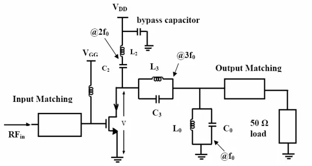
Figure 1 illustrates the basic design architecture for Class F power amplifier. VDDand VGG present the
man-datory drain and gate bias, which were determined before from a 26 V supply. DC bias and DC blocks are over-looked in this design. Input and output corresponding networks transform the impedance so the transistor, at their respective sides, should meet 50 ohms. Based on the fundamental frequency, filter combination L0C0is
tuned. It supplies very high impedance (preferably an open circuit) for the fundamental frequency, and very low impedance (preferably a short circuit) for harmonic frequencies. Together, L3and C3make the third harmonic
trap. This trap makes high impedance available for the third harmonics and permits all other signals to pass through. Therefore, the third harmonic voltages are added out of phase to the fundamental voltage at the drain, resulting in the flattening of the drain voltage waveform. The series filter combination L2C2,together
with bypass capacitor bypasses the second harmonics to
M. SABAGHI ET AL. 663
Figure 1. Class F power amplifier design architecture.
ground and, at other frequencies, provides high imped-ance. The consequence is a short circuit second harmonic current which, consecutively, makes the drain current waveform be similar to a peaked half sinusoid [3].
3. Class F Implementation
We have clarified various design blocks of the Class F amplifier. The final design was recognized in ADS. Mo-torola’s High Voltage Version 10p04 LDMOS transistor model is employed in the PA. We have applied non-ideal inductors with a Q of 20 in order for the results gained to be close to the performance gained applying commercial inductors. Identical transistors, bias points and input and output corresponding networks are used for Class F am-plifiers. Figure 2 illustrates the ultimate realization of the Class F designs respectively. These designs are then simulated with the results to be analyzed.
3.1. DC Characteristics Analysis
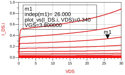
The first step in designing any power amplifier is to choose the most appropriate bias point as shown in Figure 3.
If we alter the gate and drain bias voltages, the tran-sistor's output characteristics demonstrate the different regions of operation (ohmic, saturation, and cut-off) and transistor’s transfer characteristics demonstrate the pin- ch-off voltage for definite drain bias voltage [4]. The drain voltage was altered from 0 to 30 volts, as shown in Figure 4.
We carried a DC bias point simulation out, in order to determine the bias point. The plot of the DC transfer characteristics for the transistor at a drain-source voltage of 26 V is illustrates in Figure 4.
We may notice from Figure 5 that the transistor has to be provided with a gate bias voltage between 3.2 V and 4 V for Class F operation. A 3.8 V gate bias voltage was
selected for this design. The maximum value of drain current is 340 mA, as observed. A drain voltage of VDS = 26 V was selected.
3.2. Input and Output Matching
Us Matching input and output can be provided by means of a simple discrete element matching network, like an L-network, T-network or pi-network. A pi-network, C2- L1-L2, was employed to match to 50 ohms. We applied a high pass L-network, L4-C5 for output matching to 50 ohms. The capacitive element in the output L-network works as a DC blocking capacitor too (Figure 6).
3.3. S-Parameter Simulation
Simulated S-parameters Class F power amplifier is rep-resented in Figure 7. S21 is above 20 dB at 2.14 GHz, and input and output impedance matching (S11, S22) is below –10 dB at 2.14 GHz, as shown in Figure 7. Fig-ure 8 represents Noise Figure and shows that NF is close to 2.6 dB from 1 to 3 GHz. NFmin is below 1.94 dB at 2.14 GHz.
3.4. Harmonic Terminations
The second and the third order harmonics tuning should be integrated in the output network, in Class F amplifier, in order to enlarge output power and efficiency.
Figure 2. Schematic of the Class F power amplifier design.
Figure 3. Schematic of DC bias for Class F power amplifier.
5 10 15 20 25
0 30
0.2 0.4 0.6 0.8
0.0 1.0
VDS
I_
D
S
.i
m1 m1
indep(m1)=
plot_vs(I_DS.i, VDS)=0.340 VGS=3.800000
26.000
Figure 4. IDS vs VDS.
harmonic frequency of 4.28 GHz was primarily designed for the second harmonic trap. Yet, we noticed there was considerable fourth harmonic current in the circuit, which resulted in the loss of power. A transmission line of the length of one quarter-wavelength at fundamental fre-quency was tied to the drain of the transistor, and the
2.2 2.4 2.6 2.8 3.0 3.2 3.4 3.6 3.8
2.0 4.0
0.2 0.4 0.6 0.8
0.0 1.0
VGS
I_
D
S
.i
m2 m2
indep(m2)=
plot_vs(I_DS.i, VGS)=0.340 VDS=26.000000
3.800
Figure 5.IDS vs VGS.
[image:3.595.64.283.490.622.2] [image:3.595.322.527.491.619.2]M. SABAGHI ET AL. 665
Figure 6. Input and output matching network.
Figure 7. S-parameter of Class F power amplifier.
Figure 8. Noise figure of Class F power amplifier.
the transmission line was not able to generate a good open circuit. A potential work to be done in this field may be realizing the harmonic traps on-chip with the output matching done off-chip. A line of a quarter-wavelength at 2.14 GHz might be too long to fit inside a chip. Therefore, the third harmonic trap was recognized by applying dis-crete components. We can add harmonic traps for the fifth and other higher odd harmonics in order to enhance the performance at the expense of increased circuit com-plexity. The trade-off between the number of odd har-monic traps and circuit complexity is analyzed in [5], and it is figured out that, often, the third harmonic trap is suf-ficient for acceptable Class F performance. Additional harmonic traps, in addition to increasing the circuit com-plexity, might lead to loss when realized employing prac-tical components. Moreover, it might be impossible to realize the design by means of practical components, at high operational frequencies. Bearing in mind the restric-tions mentioned, it seems that the selected design scheme for the harmonic traps is the best solution.
Figure 9 shows the PAE plots of the Class F amplifi-ers respectively. There are Maximum PAE at 21 RFpower for which PAE = 75.85.
The gain plots for Class F amplifier are represented in Figure 10.
Figure 11 illustrates a plot of the power supplied to the load, in dBm, at each frequency of the Class F power amplifier.
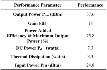
Table 1 summarizes the performance of Class F pow- er amplifier. Table 2 is comparsion of performances of various Class F Pas.
4. Conclusions
A Class-F amplifier is designed and stimulated for this paper. The amplifier was simulated by employing a high frequency circuit simulator titled as the Agilent Ad-vanced Design System (ADS). The feasibility of using a
5 10 15 20
0 25
20 40 60
0 80
RFpower
PAE
m5
m5 RFpower= PAE=75.852
21.000
Figure 9. PAE (%) vs RF power (dBm).
Figure 10. Transducer power gain (dB) vs RFpower (dBm).
2 4 6 8 10 12 14 16 18
0 20
-150 -100 -50 0
-200 50
freq, GHz
S
pect
rum
m2
m2 freq=
Spectrum=37.656 RFpower=25.000000
2.140GHz
Table 2. Comparsion of performances of various Class F Pas.
Reference fc (GHz) PAE (%) Pout (dBm) Device
[6] 2 70.5 19.85 GaAs pHEMT
[7] 2 76 21 GaAs pHEMT
[8] 1.9 63 30 GaAs FET
[9] 2.4 59 22.2 GaAs MESFET
[10] 2.14 70 40.2 GaN HEMT
This Work 2.14 75.8 37.6 LDMOS
Class F amplifier for WCDMA applications is proved via simulation, by achieving an efficiency of 75.8% with good linearity. This research provided the opportunity of making some important contributions in this field of in-vestigate. The idea of employing Class F amplifiers for improving efficiency without corrupting linearity is rather new, and there has been no significant published work which focuses on Class F amplifiers for WCDMA applications up to today. The actual performance of the designed amplifier might differ considerably.
Amplifiers,” Master’s Thesis Report, The University of Virginia, Blacksburg, 2004.
[5] F. H. Raab, “Class-F Power Amplifiers with Maximally Flat Waveforms,” IEEE Transactions on Microwave Theory and Techniques, Vol. 45, No. 11, 1997, pp. 2007-2012. doi:10.1109/22.644215
[6] M. Wren and T. J. Brazil, “Experimental Class-F Power Amplifier Design Using Computationally Efficient and Accurate Large-Signal pHEMT Model,” IEEE Transac- tions on Microwave Theory and Techniques, Vol. 53, No. 5, May 2005, pp. 1723-1731.
doi:10.1109/TMTT.2005.847108
[7] S. Gao, P. Butterworth, S. Ooi and A. Sambell, “High- Efficiency Power Amplifier Design Including Input Har- monic Termination,” IEEE Microwave and Wireless Component Letters,Vol. 16, February 2005, pp. 81-83. [8] J. Sun, B. Li and Y. W. M. Chia, “A Novel CDMA
Power Amplifier for High Efficiency and Linearity,” IEEE Proceedings of Vehicular Technology Conference, Shenzhen, 1990,pp. 2044-2047.
[9] I. Lin, M. Devincentis, C. Caloz and T. Itoh, “Arbitrary Dual-Band Components Using Composite Right/Left- Handed Transmission lines,” IEEE Transactions on Microwave Theory and Techniques, Vol. 53, April 2005, pp. 1142-1149.
[image:5.595.60.284.266.394.2]