Abstract— We present a novel compact nanophotonic device consisting of a nonclassical light source excited by a monolithically integrated and electrically driven quantum dot microlaser. Our device concept is based on self-assembled InAs quantum dots (QDs) embedded in micropillar cavities and has many potential applications in the fields of quantum communication and quantum optics-based information processing. Electrically driven micropillars act as whispering gallery mode (WGM) microlasers operable in both continuous and pulsed mode, with narrow pulse widths of 520 ps and decay constants as low as 160 ps observed. These microlasers are used as on-chip excitation sources to laterally excite individual QDs in nearby micropillars, which in turn act as vertically emitting nonclassical light sources. Our compact solid-state platform utilizes cavity-quantum electrodynamic (cQED) effects to create antibunched light in continuous and pulsed operation with g(2)CW(0) = 0.76 ± 0.03 and g(2)pulsed(0) = 0.78 ± 0.11, demonstrating its potential for the generation of triggered single photons in a highly integrated chip.
Index Terms— Photonic Integrated Circuits, Single-photon Sources, Whispering Gallery Modes, Quantum Dots
I. INTRODUCTION
The generation, manipulation, and detection of single photons on an integrated platform containing passive and active elements is actively pursued within the nanophotonics community [1]-[10]. Common methods of generating single photons often rely on probabilistic or nonlinear effects leading either to low efficiencies or potential security vulnerabilities [11], [12] as well as requiring a bulky external laser source, limiting scalability. Linear optics-based quantum information processing [13] and quantum cryptography schemes [14] utilizing, e.g., the polarization of single photons, would greatly
Manuscript received February 6, 2015. This work was supported by the German Research Society via Grant RE2974/9-1 and SCHN1376/1-1.
P. Munnelly, T. Heindel, M. M. Karow, and S. Reitzenstein are with the Institute of Solid State Physics, Technische Universität Berlin, 10623 Berlin, Germany (phone: 0049-30-314-79269; fax: 0049-30-314-22064; e-mail: [email protected]).
M. Kamp, and C. Schneider are with the Department of Technische Physik, Universität Würzburg, 97074 Würzburg, Germany.
S. Höfling is with the Department of Technische Physik, Universität Würzburg, 97074 Würzburg, Germany and with the SUPA, School of Physics and Astronomy, University of St Andrews, St Andrews, KY16 9SS, United Kingdom.
benefit from the compactness and efficiency afforded by such architectures.
A high degree of photon indistinguishability is another very desirable feature of any single-photon source (SPS), as Bell-state measurements based on two-photon interference are critical for the realization of, e.g., quantum repeaters [15]. In this context, it has been demonstrated that photons generated by solid-state quantum dots (QDs) excited in resonance with ground or higher states demonstrate reduced time jitter and dephasing [16], [17], leading to higher degrees of indistinguishability due to longer coherence times in comparison with above-band excitation methods [18], [19]. For this reason, future technologies employing highly indistinguishable photons will almost certainly rely on resonant excitation techniques, which are challenging to implement due to the large background from the excitation source. Polarization optics [20] and orthogonal detection/excitation geometries [21] can be used to suppress this background for resonant optical excitation schemes. On the other hand, an ideal SPS found in any device will also make use of a well-defined electrical trigger to deterministically deliver a single indistinguishable photon on demand. This feature, which would be most readily based on p-i-n-doped structures, is not directly compatible with the benefits afforded by resonant excitation as the charge carriers are injected and not created within the SPS. Furthermore, an electrical tuning mechanism which allows the discrete energy level of the SPS and the emission energy of the excitation source to be brought into spectral resonance will be necessary to overcome randomness inherent in fabrication to date. QDs in micropillar cavities have succeeded on these fronts separately, but not at the same time, through demonstrations of highly efficient on-demand electrically driven single-photon generation [22] in doped micropillar structures and the quantum-confined Stark effect [23] respectively. In general, nanostructures which are difficult to electrically contact, e.g., semiconductor nanowires [24]-[26], would also benefit from some sort of compact architecture converting an electrical pulse into an optical pulse which subsequently excites a nearby nonclassical emitter.
This paper reports on the emission of pulsed nonclassical light from a single QD embedded in a distributed Bragg reflector micropillar cavity which is pumped by an electrically driven whispering gallery mode (WGM) microlaser on the
A Pulsed Nonclassical Light Source
Driven by an Integrated Electrically Triggered
Quantum Dot Microlaser
Pierce Munnelly, Tobias Heindel, Matthias M. Karow
Member, IEEE
, Sven Höfling
Senior Member,
same chip. Previous experiments on a similar structure demonstrated p-shell resonant excitation and single QD cavity-quantum electrodynamic (cQED) effects in the weak-coupling regime under continuous wave (CW) excitation [27]. In this work, we study the Purcell-enhanced emission in both steady-state and time-resolved measurements via continuous and pulsed operation of the integrated microlaser. Moreover, we demonstrate for the first time the triggered emission of nonclassical light from a QD which is excited by an on-chip integrated and electrically driven microlaser.
II. TECHNOLOGY
A. Device Layout
The sample is based on a planar microcavity structure grown by molecular beam epitaxy on an n-doped (100)-oriented GaAs substrate. The active medium consists of a single layer of self-organized InAs QDs (area density ~ 109 cm-2) treated via a partial capping and annealing process [22] embedded within a one-λ thick intrinsic GaAs cavity. The latter is sandwiched between a lower n-doped and an upper p-doped distributed Bragg reflector (DBR), containing 27 and 23 λ/4 AlAs/GaAs mirror pairs, respectively. Micropillars are patterned by electron beam lithography and etched by reactive ion plasma etching. After etching, the device is planarized using the polymer bencocyclobutene (BCB) and Au pads are fabricated for electrical contacting. For details on sample growth and processing, we refer the reader to [28].
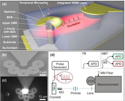
Our device based on the aforementioned technology is depicted in a schematic view in Fig. 1(a). The integrated coherent light source is realized by an electrically driven
WGM microlaser based on a micropillar cavity. WGMs are circularly propagating electromagnetic waves confined via total internal reflection at the circumference of a circular resonator, which in this device is formed by the sidewalls of the active layer of a 6.0 µm diameter micropillar. The spectral position of the WGM depends on the diameter, and the required gain for lasing is provided by the single layer of self-organized QDs in the central cavity layer. Emission of the WGM microlaser in turn laterally excites the QD layer of a monolithically integrated target micropillar with a diameter of 2.5 µm located 15 µm away. Within this high quality (Q) factor low mode-volume peripheral micropillar, QDs are excited and emit into vertical pillar modes whose highly directional emission (beam divergence ~ 10° [29]) can be detected with a microscope objective aligned in parallel to the growth axis. Due to the smaller diameter of the peripheral micropillar and the inhomogeneous broadening of the QD ensemble, only a small number of QDs (~ 10) effectively interact with the confined fundamental optical mode, allowing for the observation of cQED effects in the single emitter regime. To achieve high signal-to-background ratios, integrated micro-apertures (12.5 µm outer diameter) at the target micropillar are a crucial feature which very effectively suppress stray light from the WGM laser in combination with a pinhole configuration in the detection path of the experimental setup. Much attention also has to be devoted to the optimization of the growth conditions for the QD ensemble, to ensure sufficient gain for lasing is available and that lasing occurs at wavelengths about 20-35 nm shorter than the spectral position of the fundamental cavity modes in the external pillars. Fig. 1(b) depicts a scanning-electron microscopy image of a fully processed device, and an optical microscopy image of such a device in operation with the WGM microlaser being electrically driven can be seen in Fig. 1(c).
B. Experimental Setup
Processed devices are characterized via micro-electroluminescence (µEL) and micro-photoluminescence (µPL) spectroscopy with high spatial and spectral resolution in a configuration outlined in Fig. 1(d). The sample is mounted in a liquid-Helium flow cryostat at cryogenic temperatures (15 K) and contacted electrically via Au wire bonds connected to impedance-matched coaxial cables. Integrated WGM microlasers can be excited electrically via a source-measurement unit for direct current (dc) injection or via an electrical pulse generator for pulsed current injection. The latter provides short electrical voltage pulses with a full-width at half-maximum (FWHM) of 500 ps and fall times as short as 250 ps at a repetition rate of up to 250 MHz. Luminescence from the sample is collected using a 20x microscope objective (MO) with a numerical aperture of 0.42. After spatial filtering via a 30 μm diameter pinhole for stray-light suppression, the collimated beam is then focused onto the entrance slit of a triple-grating monochromator, which can be operated either in subtractive mode for large spectral coverage or in additive mode for high resolution with a limit of 85 µeV and 35 µeV, respectively. Spectra are recorded with a liquid nitrogen-cooled charge coupled device (CCD) camera. For time-Fig. 1. Device layout and experimental setup for the generation of
[image:2.612.48.296.49.249.2]resolved (TR) measurements, a multi-mode (MM) fiber is coupled to an avalanche photodiode (APD) with either 40 ps or 340 ps timing resolution attached to the second output port of the monochromator. Photon autocorrelation measurements are carried out to examine the photon statistics of the sample using a 50:50 MM fiber-coupled beamsplitter (BS) and two high quantum-efficiency APDs in a Hanbury-Brown and Twiss (HBT) type setup with an overall timing resolution of 480 ps. Both HBT and TR setups utilize time-correlated single-photon counting (TCSPC) electronics for coincidence measurements.
III. ON-CHIP EXPERIMENTS
A. WGM Microlaser Under Direct Current Injection
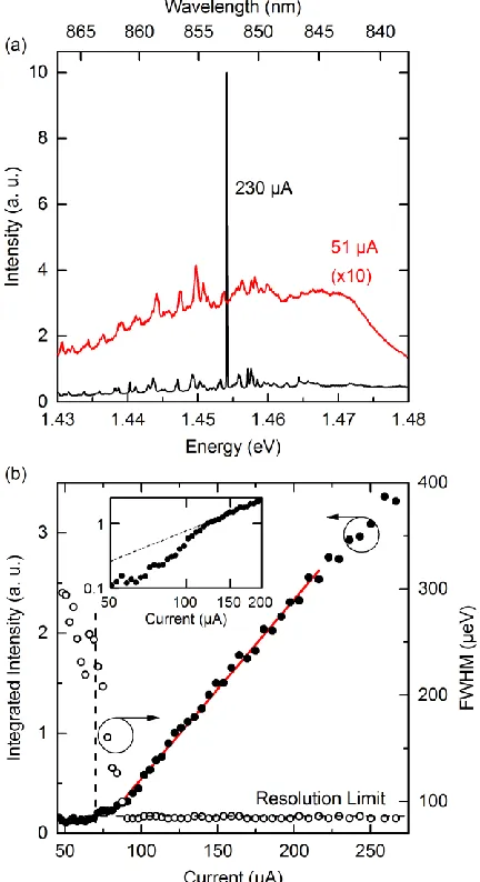
The emission characteristics of an integrated WGM microlaser with a diameter of 6 m were first evaluated under dc injection at a temperature of 15 K. In Fig. 2(a), low and high current µEL spectra of the microlaser are displayed. At low pump currents, the spectrally broad emission of the QD ensemble dominates the spectrum and distinct WGMs are hardly visible. In contrast, at high current injection the microlaser’s emission is dominated by one bright and resolution-limited WGM at 1.454 eV (853 nm). The input/output characteristic of this mode is evaluated for a wide range of currents in Fig. 2(b), with the integrated intensity and FWHM extracted from Voigt fits to the µEL spectra. At low injection currents, the linewidth of the WGM is about 0.3 meV. Increasing the injection current results in a distinct decrease in linewidth, which finally reaches the resolution limit of the setup (85 µeV) for currents above 90 µA. The drop in linewidth is accompanied by a rapid increase of the integrated WGM intensity, revealing a threshold current of
Ith = 70 µA obtained from a linear fit to the data (solid straight line). In particular, the smooth s-shape of the input/output curve in logarithmic scaling (cf. inset of Fig. 2(b)) indicates a high -factor, implying that a high fraction of the spontaneous emission is coupled into the WGM lasing mode – a feature specific to high-Q low mode-volume microcavity structures [30]-[32].
B. Pulsed Operation of WGM Laser and Target Micropillar
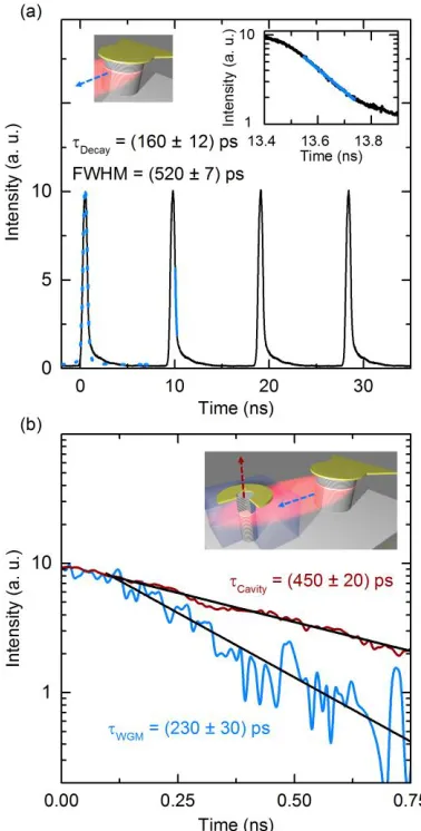
With respect to applications, pulsed operation of our integrated device is a desirable feature. We first investigated the optical response of a WGM microlaser (6.0 µm diameter) to narrow electrical pulses using the TR setup (cf. Fig. 1(d)) by spectrally selecting the lasing WGM emission and passing it onto an APD with 40 ps timing resolution. The corresponding TR data can be seen in Fig. 3(a). A pulsed voltage source was used to deliver pulses with an FWHM of 770 ps, a fall time of 250 ps, a pulse amplitude of 9 V, and a dc offset of 7 V to the contacts of the microlaser with a pulse repetition rate of 107 MHz. The TCSPC electronics were triggered directly by the pulse generator. These conditions correspond to pulses which modulate the WGM microlaser along the input/output curve from just below the threshold (~ 8.1 V) to well above threshold. The dc bias is also necessary to efficiently inject charge carriers into the active region of the p-i-n-doped cavity structure. A train of narrow optical pulses (FWHM = 520 ps) with a period of 9.3 ns, corresponding to the applied pulse repetition rate, is observed. Displaying the TR data in a semi-logarithmic plot, as seen in the inset of Fig. 3(a), reveals a time constant of τDecay = 160 ps for the falling edge of the pulses. Interestingly, a decay curve with a longer time constant of ~ 1.2 ns can be seen at later times on the tail of each pulse, which might be related to a reduced coherence and the return to spontaneous emission processes [33].
Next, we investigated the optical response of a peripheral target micropillar with a diameter of 2.5 µm under pulsed lateral on-chip excitation via a 6.0 µm diameter WGM Fig. 2. Optical characteristics of a 6 μm diameter WGM microlaser at
[image:3.612.63.279.55.452.2]microlaser connected to the pulse generator as described above. The voltage pulses were delivered with a frequency of 188 MHz, a width of 530 ps, a fall time of 370 ps, and 10 V in amplitude. A bias voltage of 6.5 V was applied with the pulses spanning the input/output curve starting at just below threshold (7.3 V, 70 µA). Fig. 3(b) shows the time-resolved measurement data recorded on stray light from the WGM microlaser (blue, light) along with the corresponding vertical emission of the fundamental optical mode at 1.407 eV (881 nm) of the target micropillar (red, dark). A monoexponential fit to the data, shown in semi-logarithmic scaling, reveals a time constant of WGM = 230 ps for the WGM microlaser and a slightly longer decay constant of
Cavity = 450 ps for the target micropillar’s optical mode. This fast optical response of the target micropillar following the microlaser demonstrates the applicability of our integrated microlaser concept for triggered on-chip excitation of QD
micropillars, furthering the development of integrated pulsed SPSs.
C. Purcell Enhanced Emission of the Target Micropillar
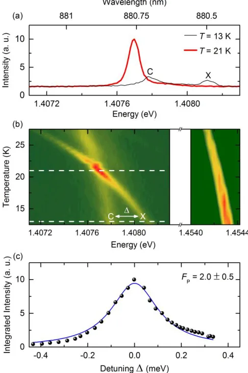
In this section, we describe detailed studies on the properties of a peripheral target micropillar performed under lateral excitation via the WGM microlaser emitting at 853 nm at 13 K. As the growth conditions of the QD layer and the geometry of the micropillars were optimized so as to allow for both lasing as well as the observation of single QD transitions, we now examine the target micropillar in the single emitter regime under low excitation from the WGM microlaser. Under these conditions, a single QD optically driven by the WGM interacts resonantly with the fundamental optical mode of its micropillar. Fig. 4(a) presents µPL spectra of a target micropillar under CW WGM microlaser excitation at two different temperatures. At a temperature of 13 K, the emission of the fundamental optical mode (C) with a Q-factor of 8300 is identified at EC = 1.4078 eV. In addition, a single QD exciton (X) emission line is visible at 1.4081 eV, which results from the recombination of a QD-confined electron-hole pair. By exploiting the temperaturedependence of the semiconductor’s bandgap, X can be tuned into spectral resonance with C at
T = 21 K (red line), resulting in a distinct enhancement of the QD peak intensity by a factor of 3.7 (average CCD count rates: 300 Hz and 80 Hz on- and off- resonance, respectively). As we will show later, this increase in emission rate of the coupled QD-cavity system is due to a reduced exciton lifetime, which is a direct consequence of the Purcell effect in the regime of weak light-matter interaction. This effect is further illustrated in a contour plot displaying µPL spectra of the target micropillar driven by the WGM microlaser for a wider temperature range as seen in Fig. 4(b) (left panel). Starting from T = 12 K, the X emission shifts to lower energies with increasing temperature. The spectral position of X coincides with that of the optical mode C at a resonance temperature of 21 K. µEL spectra of the WGM microlaser are also displayed as a contour plot in the right panel of Fig. 4(b), demonstrating the stability of the WGM over the corresponding temperature range. To gain quantitative insight into the observed cQED effect, we fitted Lorentzian lineshapes to the optical mode C and the exciton emission X. Fig. 4(c) shows the extracted integrated emission intensity of X as a function of the spectral detuning between X and C. The data clearly reflect a Lorentzian profile corresponding to the modified optical density of states of the fundamental cavity mode. We model the integrated exciton intensity according to [34], where FP is the Purcell factor, is the detuning of the QD transition from the cavity resonance, and C = EC/Q = 0.17 meV is the cavity FWHM. This allows for a Purcell factor FP = 2.0 0.5 to be determined, which implies a reduction of the exciton’s radiative lifetime by a factor of two. It is interesting to compare this result with the highest achievable Purcell factor , where VM denotes the effective mode volume and the effective refractive index [35]. From this we gain an upper limit for the Purcell factor of 15 for the present cavity (Q = 8300, VM = 0.83 µm3 [28]). The lower experimental FP can be explained by a spatial mismatch Fig. 3. Optical response of a WGM microlaser under pulsed electrical
[image:4.612.78.267.53.426.2]of the QD with respect to the field maximum of the confined mode [36], [37].
To directly observe the Purcell effect in this system in terms of a modification of the emitter’s spontaneous lifetime, we performed time resolved measurements on the emission of this single QD exciton X in dependence of the spectral detuning . The WGM microlaser excitation source was again used in pulsed operation via the electrical pulse generator. The measured optical decay of the X emission is presented in Fig. 5(a) and (b) in logarithmic scaling for a spectral detuning close to resonance ( = 16 µeV) and far from resonance ( = 105 µeV), respectively. The experimental data reveal a significant reduction in the exciton’s decay time from 650 ps out of resonance to 500 ps close to resonance. The relatively low signal-to-noise ratio is related to the low emission rate of the peripheral micropillar in conjunction with the utilized fast
Si-APDs (40 ps timing resolution) featuring a low detection efficiency (~ 5 %) in the spectral region of interest. Fig. 5(c) plots the X decay times extracted for various spectral detunings and clearly confirms the reduction of the radiative lifetime due to the emitter’s interaction with the fundamental optical mode. Also, judging from the Purcell factor determined in Fig. 4(c), the reduction in the emitter’s radiative lifetime might be expected to be more pronounced. However, the rather moderate impact on the measured time constants can be explained by spectral background contributions from so-called “spectator” QDs emitting non-resonantly into the optical mode C [34], an interpretation which is also confirmed by photon statistics measurements in the following section.
D. Nonclassical Light Generation
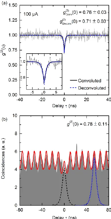
Based on the findings of the previous sections, we now examine the photon statistics of the resonantly coupled QD-cavity system investigated in the last paragraph to explore its potential for the generation of triggered single photons in the framework of our highly integrated device approach. The Purcell-enhanced QD emission (cf. Fig. 4(a)) was coupled into the MM-fiber and guided to the HBT setup for coincidence measurements of the photon autocorrelation function g(2)(). The WGM microlaser excitation source was initially operated in CW mode at an injection current slightly above threshold of 100 µA, chosen for the best signal-to-background ratio of the target micropillar’s emission. The resulting g(2)() histogram is Fig. 4. Micro-photoluminescence (µPL) spectra of a peripheral target
micropillar under lateral continuous wave (CW) excitation via an electrically pumped integrated WGM microlaser. (a) Emission of a single QD exciton (X) is tuned into spectral resonance with the fundamental optical mode (C) of the micropillar at 21 K. The observed enhancement of the X emission is attributed to the Purcell effect in the weak light-matter coupling regime. (b) Contour plot of µPL spectra in a broader temperature range, illustrating the resonance tuning and the corresponding emission enhancement within the target micropillar (left). On the right side of the panel, the lasing mode of the exciting WGM microlaser is shown over the same temperature range. (c) Normalized integrated µPL intensity of the X emission line as a function of spectral detuning between X and C. Modeling of the data (blue curve) yields a Purcell factor FP = 2.0 0.5.
[image:5.612.321.565.49.329.2] [image:5.612.55.298.56.421.2]depicted in Fig. 6(a). At zero time delay ( = 0), a pronounced dip is visible indicating antibunching of the emitted light. This corresponds to the suppression of two-photon emission events, and analysis of the data according to [38] yields a measured value of g(2)Conv(0) = 0.76 0.03. Considering the finite timing resolution of the HBT setup (480 ps), we extract a deconvoluted value of g(2)Deconv(0) = 0.71 0.03 as plotted in the inset of Fig. 6(a). The observed antibunching is a clear demonstration of nonclassical light generation. However,
g(2)(0) still deviates from what is expected of a perfect single-photon emitter (g(2)(0) = 0), which can mainly be explained by the uncorrelated background emission of the fundamental optical mode [22]. For the present case, we estimate a ratio
=S/(S+B) of the single emitter (S) to total spectral contributions (S+B) of 0.49 by examining the on- and off- resonance spectra. According to [38] this leads to an expected value of g(2)B(0) = 0.76 caused by the background B, which is in very good agreement with the experimental value.
Finally, by switching to pulsed operation of the WGM microlaser, we tested our device for triggered generation of nonclassical light at a repetition rate of 96 MHz. The corresponding autocorrelation histogram is displayed in Fig. 6(b). A periodic sequence of coincidence maxima is observed due to the pulsed excitation by the WGM microlaser. The peak area at = 0 is noticeably reduced in comparison with those at finite time delays, reflecting the antibunching characteristic of nonclassical light generation. The considerable background observed in this measurement can be explained by a second longer time constant of the optical pulses, leading to an overlap of neighboring coincidence maxima. The experimental data are modeled as a sequence of coincidence maxima, where each peak is described by the TR decay measurement performed on the QD convoluted with itself. Assuming different peak heights at vanishing and finite time delay , as well as the decay time of the coincidence maxima of 2.5 ns, the data are nicely described by the fit curve (red line). By computing the ratio of the central peak area to the average area of the side peaks, we deduce
g(2)(0) = 0.78 ± 0.11, in good agreement with photon autocorrelation measurement under CW excitation (cf. Fig. 6(a)).
IV. CONCLUSION
This work demonstrates the feasibility of realizing nanophotonic devices utilizing highly integrated microlasers as on-chip coherent light sources for the generation of triggered single photons. The results presented in section III.D are summarized in Table I. Future work will focus on better suppression of multiphoton emission events and improved photon out-coupling efficiencies of the external micropillars, which might lead to highly-integrated bright sources of indistinguishable photons. Firstly, the g(2)(0) value can be improved by reducing the spectral density of QDs close to the fundamental optical mode of the peripheral micropillar. This issue can be tackled by growing samples with a small inhomogeneous broadening of the QD ensemble emission, which ensures both, sufficient optical gain for the WGM laser and a low spectral density of single QD emission lines close to the cavity mode of sufficiently detuned peripheral micropillars. Secondly, technologically more demanding, single site-controlled QDs [39] could be integrated into the Fig. 6. Photon statistics measurements on the resonantly coupled QD-cavity
system of a peripheral target micropillar under lateral on-chip excitation via a WGM microlaser. Shown are the photon autocorrelation g(2)() under (a) CW microlaser excitation and (b) pulsed microlaser operation. Solid/dashed curves represent fits to the data explained in the main text. Both measurements clearly demonstrate, for the first time, the generation of nonclassical light (g(2)(0) < 1) from a QD excited by an on-chip integrated coherent light source.
TABLEI
WGM Microlaser Target Micropillar
Energy 1.4543 eV 1.4077 eV
FWHM < 35 µeV Cavity: 170 µeV Exciton: 75 µeV
Decay (230 30) ps (450 20) ps
FWHM (730 20) ps (980 33) ps
FP = 2.0 0.5 g(2)
CW(0) = 0.71 0.03 g(2)
Pulsed(0) = 0.78 0.11
[image:6.612.320.540.49.186.2] [image:6.612.78.273.53.435.2]peripheral micropillars while QDs with a higher surface density could act as gain medium for the central WGM microlaser. To improve the performance of our concept in terms of the single-photon emission rate, an optimized microcavity design with a lower number of mirror pair in the upper DBR can be implemented, which allows for optimization of the photon extraction efficiency for a given range of the peripheral target micropillar diameter [22]. Moreover, improvements on stray light suppression and efficient guiding of WGM emission to target micropillars are being investigated which can pave the way for fully integrated on-chip resonance fluorescence studies. A promising approach in this respect is the application of Limaçon-shaped geometries of the WGM microlaser, enabling highly directional WGM emission [40]. Further work is also being carried out to eliminate the need for temperature-tuning via the quantum-confined Stark effect, whereby the external micropillar apertures are electrically contacted. Our device layout also naturally lends itself to the very desirable integration of arrays of single-photon sources. Future work investigating the viability of these microlasers for the generation of entangled photon pairs via spontaneous parametric down-conversion within integrated GaAs waveguides [41] seem to be within reach. We believe the results presented here demonstrate that our device has great potential for applications in the field of nanophotonics.
ACKNOWLEDGMENT
The authors gratefully acknowledge expert sample preparation by M. Lermer, M. Emmerling, and A. Wolf.
REFERENCES
[1] D. Englund, A. Faraon, B. Zhang, Y. Yamamoto, and J. Vuckovic, “Generation and transfer of single photons on a photonic crystal chip,” Opt. Express, vol. 15, pp. 5550–5558, Apr. 2007.
[2] J. C. F. Matthews, A. Politi, A. Stefanov, and J. L. O’Brien, “Manipulation of multiphoton entanglement in waveguide quantum circuits,” Nature Photon., vol. 3, pp. 346–350, May 2009.
[3] J. P. Sprengers, A. Gaggero, D. Sahin, S. Jahanmirinejad, G. Frucci, F. Mattioli, R. Leoni, J. Beetz, M. Lermer, M. Kamp, S. Höfling, R. Sanjine, and A. Fiore, “Waveguide superconducting single-photon detectors for integrated quantum photonic circuits,” Appl. Phys. Lett., vol. 99, pp. 181110-1–181110-3, Nov. 2011.
[4] A. Laucht, S. Pütz, T. Günthner, N. Hauke, R. Saive, S. Frédérick, M. Bichler, M.-C. Amann, A. W. Holleitner, M. Kaniber, and J. J. Finley, “A waveguide-coupled on-chip single-photon source,” Phys. Rev. X, vol. 2, pp. 011014-1–011014-7, Mar. 2012.
[5] T. B. Hoang, J. Beetz, M. Lermer, L. Midolo, M. Kamp, S. Höfling, and A. Fiore, “Widely tunable, efficient on-chip single photon sources at telecommunication wavelengths,” Opt. Express, vol. 20, pp. 21758– 21765, Sep. 2012.
[6] A. Faraon, C. Santori, Z. Huang, K.-M. C. Fu, V. M. Acosta, D. Fattal, and R. G. Beausoleil, “Quantum photonic devices in single-crystal diamond,” New J. Phys., vol. 15, pp. 025010-1–025010-9, Feb. 2013. [7] A. W. Schell, J. Kaschke, J. Fischer, R. Henze, J. Wolters, M. Wegener,
and O. Benson, “Three-dimensional quantum photonic elements based on single nitrogen vacancy-centres in laser-written microstructures,” Sci. Rep., vol. 3, pp. 1577-1–1577-5, Apr. 2013.
[8] G. Reithmaier, S. Lichtmannecker, T. Reichert, P. Hasch, K. Muller, M. Bichler, R. Gross, and J. J. Finley, “On-chip time resolved detection of quantum dot emission using integrated superconducting single photon detectors,” Sci. Rep., vol. 3, pp. 1901-1–1901-6, May 2013.
[9] A. Jamil, J. Skiba-Szymanska, S. Kalliakos, A. Schwagmann, M. B. Ward, Y. Brody, D. J. P. Ellis, I. Farrer, J. P. Griffiths, G. A. C. Jones,
D. A. Ritchie, and A. J. Shields, “On-chip generation and guiding of quantum light from a site-controlled quantum dot,” Appl. Phys. Lett., vol. 104, pp. 101108-1–101108-4, Mar. 2014.
[10] M. Makhonin, J. Dixon, R. Coles, B. Royall, I. J. Luxmoore, E. Clarke, M. Hugues, M. Skolnick, and A. M. Fox, “Waveguide coupled resonance fluorescence from on-chip quantum emitter,” Nano Lett., vol. 14, pp. 6997–7002, Nov. 2014.
[11] N. Lütkenhaus, “Security against individual attacks for realistic quantum key distribution,” Phys. Rev. A, vol. 61, pp. 052304-1–052304-10, Apr. 2000.
[12] E. Waks, C. Santori, and Y. Yamamoto, “Security aspects of quantum key distribution with sub-Poisson light,” Phys. Rev. A, vol. 66, pp. 042315-1–042315-7, Oct. 2002.
[13] E. Knill, R. Laflamme, and G. J. Milburn, “A scheme for efficient quantum computation with linear optics,” Nature, vol. 409, pp. 46–52, Jan. 2001.
[14] N. Gisin, G. Ribordy, W. Tittel, and H. Zbinden, “Quantum cryptography,” Rev. Mod. Phys., vol. 74, pp. 145–195, Jan. 2002. [15] N. Sangouard, C. Simon, J. Minář, H. Zbinden, H. de Riedmatten, and
N. Gisin, “Long-distance entanglement distribution with single-photon sources,” Phys. Rev. A, vol. 76, pp. 050301-1–050301-4, Nov. 2007. [16] H. S. Nguyen, G. Sallen, C. Voisin, Ph. Roussignol, C. Diederichs, and
G. Cassabois, “Ultra-coherent single photon source,” Appl. Phys. Lett., vol. 99, pp. 261904-1–261904-3, Dec. 2011.
[17] C. Matthiesen, A. N. Vamivakas, and M. Atatüre, “Subnatural linewidth single photons from a quantum dot,” Phys. Rev. Lett., vol. 108, pp. 093602-1–093602-4, Feb. 2012.
[18] Y.-M. He, Y. He, Y.-J. Wei, D. Wu, M. Atatüre, C. Schneider, S. Höfling, M. Kamp, C.-Y. Lu, and J.-W. Pan, “On-demand semiconductor single-photon source with near-unity indistinguishability,” Nat. Nanotechnol., vol. 8, pp. 213–217, Feb. 2013. [19] P. Gold, A. Thoma, S. Maier, S. Reitzenstein, C. Schneider, S. Höfling,
and M. Kamp, “Two-photon interference from remote quantum dots with inhomogeneously broadened linewidths,” Phys. Rev. B, vol. 89, pp. 035313-1–035313-7, Jan. 2014.
[20] A. V. Kuhlmann, J. Houel, D. Brunner, A. Ludwig, D. Reuter, A. D. Wieck, and R. J. Warburton, “A dark-field microscope for background-free detection of resonance fluorescence from single semiconductor quantum dots operating in a set-and-forget mode,” Rev. Sci. Instrum., vol. 84, pp. 073905-1–073905-7, Jul. 2013.
[21] S. Ates, S. M. Ulrich, S. Reitzenstein, A. Löffler, A. Forchel, and P. Michler, “Post-selected indistinguishable photons from the resonance fluorescence of a single quantum dot in a microcavity,” Phys. Rev. Lett., vol. 103, pp. 167402-1–167402-4, Oct. 2009.
[22] T. Heindel, C. Schneider, M. Lermer, S. H. Kwon, T. Braun, S. Reitzenstein, S. Höfling, M. Kamp, and A. Forchel, “Electrically driven quantum dot-micropillar single photon source with 34% overall efficiency,” Appl. Phys. Lett., vol. 96, pp. 011107-1–011107-3, Jan. 2010.
[23] C. Kistner, T. Heindel, C. Schneider, A. Rahimi-Iman, S. Reitzenstein, S. Höfling, and A. Forchel, “Demonstration of strong coupling via electro-optical tuning in high-quality QD-micropillar systems,” Opt. Express, vol. 16, pp. 15006–15012, Sep. 2008.
[24] J. Claudon, J. Bleuse, N. S. Malik, M. Bazin, P. Jaffrennou, N. Gregersen, C. Sauvan, P. Lalanne, and J.-M. Gérard, “A highly efficient single-photon source based on a quantum dot in a photonic nanowire,” Nature Photon., vol. 4, pp. 174–177, Jan. 2010.
[25] N. Gregersen, T. R. Nielsen, J. Mørk, J. Claudon, and J.-M. Gérard, “Designs for high-efficiency electrically pumped photonic nanowire single-photon sources,” Opt. Express, vol. 18, pp. 21204–21218, Sep. 2010.
[26] J. Heinrich, A. Huggenberger, T. Heindel, S. Reitzenstein, S. Höfling, L. Worschech, and A. Forchel, “Single photon emission from positioned GaAs/AlGaAs photonic nanowires,” Appl. Phys. Lett., vol. 96, pp. 211117-1–211117-3, May 2010.
[27] E. Stock, F. Albert, C. Hopfmann, M. Lermer, C. Schneider, S. Höfling, A. Forchel, M. Kamp, and S. Reitzenstein, “On-chip quantum optics with quantum dot microcavities,” Adv. Mater., vol. 25, pp. 707–710, Feb. 2013.
[29] H. Rigneault, J. Broudic, B. Gayral, and J.-M. Gérard, “Far-field radiation from quantum boxes located in pillar microcavities,” Optics Letter, vol. 26, pp. 1595–1597, Oct. 2001.
[30] H.-G. Park, S.-H. Kim, S.-H. Kwon, Y.-G. Ju, J.-K. Yang, J.-H. Baek, S.-B. Kim, and Y.-H. Lee, “Electrically driven single-cell photonic crystal laser,” Science, vol. 305, pp. 1444–1447, Sep. 2004.
[31] S. Strauf, K. Hennessy, M. T. Rakher, Y.-S. Choi, A. Badolato, L. C. Andreani, E. Hu, P. Petroff, and D. Bouwmeester, “Self-tuned quantum dot gain in photonic crystal lasers,” Phys. Rev. Lett., vol. 96, pp. 127404-1–127404-4, Mar. 2006.
[32] S. Reitzenstein, T. Heindel, C. Kistner, A. Rahimi-Iman, C. Schneider, S. Höfling, and A. Forchel, “Low threshold electrically pumped quantum dot-micropillar lasers,” Appl. Phys. Lett., vol. 93, 061104-1– 061104-3, Aug. 2008.
[33] M. Aßmann, F. Veit, M. Bayer, C. Gies, F. Jahnke, S. Reitzenstein, S. Höfling, L. Worschech, and A. Forchel, “Ultrafast tracking of second-order photon correlations in the emission of quantum-dot microresonator lasers,” Phys. Rev. B, vol. 81, pp. 165314-1–165314-5, Apr. 2010. [34] M. Munsch, A. Mosset, A. Auffèves, S. Seidelin, J. P. Poizat,
J.-M. Gérard, A. Lemaître, I. Sagnes, and P. Senellart, “Continuous-wave versus time-resolved measurements of Purcell factors for quantum dots in semiconductor microcavities,” Phys. Rev. B, vol. 80, pp. 115312-1– 115312-8, Sep. 2009.
[35] J.-M. Gérard, B. Sermage, B. Gayral, B. Legrand, E. Costard, and V. Thierry-Mieg, “Enhanced spontaneous emission by quantum boxes in a monolithic optical microcavity,” Phys. Rev. Lett., vol. 81, pp. 1110– 1113, Aug. 1998.
[36] S. Reitzenstein, C. Hofmann, A. Löffler, A. Kubanek, J.-P. Reithmaier, M. Kamp, V. D. Kulakovskii, L. V. Keldysh, T. L. Reinecke, and A. Forchel, “Strong and weak coupling of single quantum dot excitons in pillar microcavities,” phys. stat. sol. (b), vol. 243, pp. 2224–2228, Jul. 2006.
[37] C. Kistner, S. Reitzenstein, C. Böckler, R. Debusmann, J. Claudon, L. Grenouillet, S. Höfling, J.-M. Gérard, and A. Forchel, “Weak coupling effects in high-Q electrically driven micropillars,” phys. stat. sol. (c), vol. 6, pp. 381–384, Jul. 2008.
[38] P. Michler, A. Imamoğlu, A. Kiraz, C. Becher, M. Masona, P. Carson, G. Strouse, S. Buratto, W. Schoenfeld, and P. Petroff, “Nonclassical radiation from a single quantum dot,” phys. stat. sol. (b), vol. 229, pp. 399–405, Jan. 2002.
[39] C. Schneider, T. Heindel, A. Huggenberger, P. Weinmann, C. Kistner, M. Kamp, S. Reitzenstein, S. Höfling, and A. Forchel, “Single photon emission from a site-controlled quantum dot-micropillar cavity system,” Appl. Phys. Lett., vol. 94, pp. 111111-1–111111-3, Mar. 2009.
[40] F. Albert, C. Hopfmann, A. Eberspächer, F. Arnold, M. Emmerling, C. Schneider, S. Höfling, A. Forchel, M. Kamp, J. Wiersig, and S. Reitzenstein, “Directional whispering gallery mode emission from Limaçon-shaped electrically pumped quantum dot micropillar lasers,” Appl. Phys. Lett., vol. 101, 021116-1–021116-4, Jul. 2012.
[41] R. Horn, P. Abolghasem, B. J. Bijlani, D. Kang, A. S. Helmy, and G. Weihs, “Monolithic source of photon pairs,” Phys. Rev. Lett., vol. 108, pp. 153605-1–153605-5, Apr. 2012.
Pierce Munnelly completed a Master’s degree in
physics at the Free University of Berlin, Berlin, Germany in 2012. Having focused on a theoretical treatment of entanglement in semiconductor quantum dot-based systems in conjunction with the Technical University of Berlin, Berlin, Germany, he is currently working there to obtain his PhD specializing in the field of integrated nanophotonics using semiconductor quantum dot-based technologies.
Mr. Munnelly is a member of the German Physical Society (DPG).
Tobias Heindel received the Diploma degree in
physics in 2009 from the University of Würzburg, Würzburg, Germany, where he also received his PhD degree on the topic “Electrically Pumped Quantum-Dot Single-Photon Sources for Quantum Communication” at the Department Technische Physik in 2014.
He is currently working as a post-doctoral researcher at the Institute of Solid State Physics at the Technical University Berlin, Berlin, Germany. His current research interests include the realization of nonclassical light sources for quantum information and the exploration of long-lived excitonic qubits in deterministic quantum dot microstructures.
Dr. Heindel is a member of the German Physical Society (DPG).
Matthias Karow (M’13) graduated from Göttingen
University, Göttingen, Germany with a Bachelor’s degree in physics in 2011. Upon being awarded a Fulbright Scholarship, he joined Arizona State University, Tempe, AZ, USA and earned a Master’s degree in Electrical Engineering from this institution in 2014.
Currently, he is with the Optoelectronics and Quantum Device research group at Technical University Berlin, Berlin, Germany. His experience includes epitaxial growth, defect creation characterization, and quantum optics in III-V semiconductor nanostructures as well as optoelectronic applications of (AlInGa)N compounds at OSRAM Opto Semiconductors, Regensburg, Germany.
Mr. Karow is a member of the German Physical Society (DPG) and the HKN Engineering Honor Society.
Sven Höfling (M’04-SM’13) was born in 1976. He
received his diploma degree in Applied Physics from the University of Applied Science in Coburg and his PhD degree from University of Würzburg, Würzburg, Germany. He was with the Fraunhofer Institute of Applied Solid-State Physics, Freiburg, Germany from 2001 to 2002 working on blue and white light emitting diodes. In 2003, he joined Würzburg University for his PhD work on single mode emitting GaAs/AlGaAs quantum cascade lasers. From 2006 to 2013, he was head of the Optoelectronic Materials and Devices Group at Technische Physik, Würzburg University.
He is now a professor of physics at the University of Würzburg, Germany, and the University of St Andrews, Scotland. His research interests include the design, fabrication, and characterization of low-dimensional electronic and photonic nanostructures, including quantum wells and quantum dots, organic semiconductors, high-quality factor microcavities, photonic crystal devices, semiconductor lasers, organic optoelectronics, and transition metal oxides.
Dr. Höfling is a member of the IEEE Photonics Society, the German Physical Society (DPG), the European Physical Society (EPS), the Institute of Physics (IOP), and the Optical Society (OSA).
Martin Kamp received his Master’s degree from
Stony Brook University, Stony Brook, NY, USA, in 1995 and joined the Department of Technische Physik in 1996. He obtained his PhD degree from University of Würzburg, Würzburg, Germany in 2003 for his work on laterally coupled distributed feedback lasers. Since then, he is responsible for the nanofabrication and nanophotonic research at the Department Technische Physik and the Gottfried-Landwehr Laboratory for Nanotechnology, University of Würzburg, Würzburg, Germany. From 2010 to 2015, he was an Interims Chair at the department Technische Physik. He has authored or co-authored over 250 papers relating to semiconductor nanostructures, opto- and nano-electronic devices, and semiconductor spectroscopy.
His current research interests include low-dimensional electronic and photonic semiconductor structures and the development of semiconductor based optical quantum information processing and interband cascade lasers.
Christian Schneider is currently head of the spectroscopy and the polariton group at the Department Technische Physik, University of Würzburg, Würzburg, Germany. He received his PhD degree at the University of Würzburg. He spent one year at the University of British Columbia, two months at the Tecnologico de Monterrey, Mexico as undergraduate student/researcher and three months at Stanford University as visiting post-doctoral researcher. He is author or co-author of more than 100 papers, four invited book chapters relating to polaritonic research, semiconductor nanostructures, optoelectronic devices, and semiconductor spectroscopy.
His current research interests include the development of innovative microcavity and polaritonic devices, spectroscopy of bosonic quantum fluids, and novel two dimensional materials.
Dr. Schneider is a member of the German physical society (DPG) and the Mediterranean Institute of Fundamental Physics.
Stephan Reitzenstein received his diploma degree
and his PhD degree (summa cum laude) from the University of Würzburg, Würzburg, Germany, in 2000 and 2005 respectively, both in Physics. In 2010 he habilitated with studies regarding optical properties of low dimensional semiconductor systems (light-matter interaction in single quantum dot micropillar systems, single-photon sources, low threshold micropillar lasers, semiconductor nanowires).
Since September 2011 he is full Professor at the Technical University of Berlin, Berlin, Germany and holds the Chair of Optoelectronics and Quantum Devices. His current research interests are in the area of nanoelectronics and quantum optics in semiconductor nanostructures.