This work looks at the development and investigation of a reinforced composite solder with low melting point. The composite solder was prepared by adding Sn-3.0Ag-0.5Cu nanoparticles into Sn-58Bi solder paste. The Sn-3.0Ag-0.5Cu nanoparticles were manufactured using a self-developed Consumable-electrode Direct Current Arc (CDCA) technique. The test FR-4 Printed Circuit Board (PCB) with Cu pad and Electroless Nickel Immersion Gold (ENIG) surface finish were fabricated, and fifty SR1206 chip resistors were mounted on pads of test PCB with the reinforced composite solder paste by using conventional surface mount technology. The differential scanning calorimetry (DSC) was used to analyze the constituent of the composite solder joint after reflow. A scanning electron microscope (SEM), transmission electron microscope (TEM) and optical microscope (OM) were employed in order to observe the morphology of nanoparticles; the microstructure of reinforced composite solder joint; the crack initiation and propagation in solder joint; and the fracture mode after shear test. The thermal cycling (TC) was carried out with a temperature range of 40C and 125C. The contact resistance of the solder joint was measured during thermal cycling, and the shear test of solder joints was performed before and after 500 thermal cycles. After the shear test, all fracture surfaces were inspected to identify the fracture mode of the composite solder joint. The results of the experiments detailed in this work indicate that the shear strength of the composite solder increased 2 times in comparison to Sn-58Bi. Meanwhile, the thermomechanical fatigue (TMF) resistance of the composite solder with 1 mass% nanoparticles was 16 times stronger than Sn-58Bi and 4 times stronger than Sn-3.0Ag-0.5Cu. However, the tendency of forming micro-cracks between nanoparticles and solder matrix and the fracture within solder was increased for solder joints with more than 3 mass% nanoparticles after thermal cycling. [doi:10.2320/matertrans.MJ201002]
(Received December 7, 2009; Accepted May 19, 2010; Published September 25, 2010)
Keywords: composite solder, nanoparticles, shear strength, thermal cycling, fracture mode
1. Introduction
Lead-free Sn-based solders have been applied in the electronic packaging industry for several years to eliminate the negative effects of lead on human health and the environment. Unfortunately, the higher melting temperature is still a critical issue for lead-free solders. It is well known that a higher melting point results in a higher processing temperature, which in turn results in higher defect rates. Though Sn-52In and Sn-58Bi solder alloys have low melting points and have been used for step soldering and in heat-sensitive devices for a long time, the high price of indium and the brittleness of Sn-58Bi limit their development.
The development of new solders that possess good mechanical and electrical performance as well as a low melting point is essential. Attempts which have proved effective have focused on adding certain nanoparticles into conventional solder paste to form a kind of composite solder. Liu et al.1) added Ag nanoparticles into Sn-Pb solder and
proved that the nanosized Ag particle-reinforced composite solder improved the creep resistance of solder joints. Hsiao et al.2) mechanically mixed Cu
6Sn5 nanopowders into
Sn-3.5Ag solder paste to form a kind of nanosized Cu6Sn5doped
Sn-Ag-Cu solder paste. Their results indicated the ball shear strength of Cu6Sn5-contained joint was higher than that of the
bare Sn-Ag-Cu one due to nanosized Cu6Sn5reinforcement.
Shi et al.3) produced a series of composite solders by blending Sn37Pb and Sn0.7Cu solder microsized powders with different volume percentages of nanosized Cu, Ag, Al2O3 and TiO2 reinforcement particles. According to their
results, the creep resistance of each composite solder was
improved. Gain et al.4)studied the effects of nanosized Ni
addition. The nanosized Ni powder was added to Sn-9Zn and Sn-8Zn-3Bi solders and the shear strength increased. Lee et al.5)found that the shear strength of eutectic Sn-Ag solder
joint could be enhanced with nano-structured polyhedral oligomeric silsesquioxanes (POSS) particles. The studies concluded that adding nanosized particulates into a conven-tional solder alloy to form a kind of composite solder was a successful method of enhancing the mechanical performance of solders joints. Shinet al.6)added SiC nanoparticles, into
Sn-58Bi low melting point solder in an attempt to form a new low melting point composite solder. From their results, the shear strength increased 13% compared to Sn-58Bi. Lin et al.7)added metal-oxide nanoparticles into tin-lead solder, and studied the influence of the addition of titanium dioxide nanopowders on the microstructure and hardness of compo-site solder.
So far, most studies of composite solder used high melting point lead-free solder as the base material, and the process temperature is still high. In addition, the mismatch of nanoparticles and base material is also a potential issue for composite solder. In this study, Sn-based alloy was used for both nanoparticles and base material in order to minimize difference between nanoparticles and base material in terms of mechanical properties, thermal properties, etc. The Sn-based Sn-3.0Ag-0.5Cu nanoparticles were successfully pre-pared by using a self developed CDCA technique. Then, the Sn-3.0Ag-0.5Cu nanoparticles were added into traditional Sn-58Bi low melting point solder paste to form a novel composite solder with low melting point. In this study, the Sn-3.0Ag-0.5Cu nanoparticles would not melt but would
disperse into the composite solder joints in the reflow process. The reliability of this nanoparticle reinforced composite lead-free solder was studied in this work, and a high mechanical and electrical performance and good thermo-mechanical fatigue resistance was observed.
2. Experimental Procedure
Sn-3.0Ag-0.5Cu nanoparticles were successfully prepared
by using a self-developed CDCA technique.8–10) The
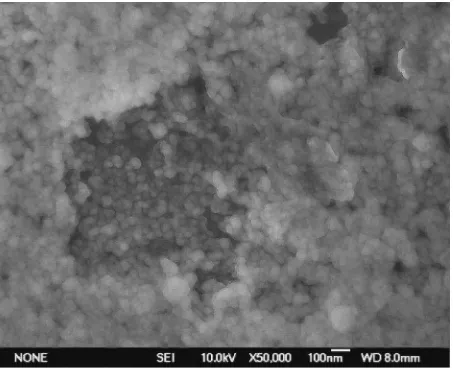
nano-particles exhibited a near spherical morphology with particle size ranging from 20 nm to 80 nm. Figure 1 show the SEM image of Sn-Ag-Cu nanoparticles which were manufactured
by the CDCA method.8)
The composite solder paste was prepared by stirring 58Bi solder paste with different weight percentages of Sn-3.0Ag-0.5Cu nanoparticles (1%, 2%, 3% and 4%) for 30 min to form a homogeneous distribution of the reinforcement particles in the original Sn-58Bi paste.
The test FR-4 PCB with ENIG/Cu pad was designed and fabricated for this study. Following the conventional surface mount technology, the chip resistors were mounted on pads of test PCB with the reinforced composite solder paste. Every PCB includes fifty SR1206 chip resistors, as shown in Fig. 2. The reflow soldering was conducted in a reflow oven with ten different temperature zones. For composite solder, a
temper-ature profile with a peak tempertemper-ature of 180C and a total
duration time of 6 min was used. The dwell time above the melting temperature of Sn-58Bi solder was approximately 60 s. In this study, the Sn-3.0Ag-0.5Cu nanoparticles did not melt but dispersed into the composite solder joints in the
reflow process, as the melting point (217C) of
Sn-3.0Ag-0.5Cu alloy is higher than peak reflow soldering temperature
(180C) of composite solder. Then, the samples were
air-cooled until they reached room temperature. The pure Sn-58Bi and Sn-3.0Ag-0.5Cu solders without nanoparticles were also used for comparing with the composite solder. The process of Sn-58Bi soldering is the same as for composite
solder. For Sn-3.0Ag-0.5Cu, the peak temperature is 245C
and the dwell time above the melting temperature of Sn-3.0Ag-0.5Cu solder is 65 s.
The constituent of the composite solder joint after reflow was analyzed by DSC. 4.66 mg of the composite solder joint of with 3 mass% nanoparticles loading was prepared and put into the DSC cell. Dynamic scanning was carried out with
a heat rate of 5C/min from 50 to 300C at a nitrogen
atmosphere.
For evaluating the effect of thermal cycling on contact resistance, shear strength and fracture mode of the composite solder, the test samples were divided into two groups. For one group, shear test was carried out directly after soldering, whereas another group endured 500 cycles of thermal cycling before the shear test. The contact resistance was measured during thermal cycling. All 12 cases (see Table 1) were studied in the present work.
Thermal cycling was carried out in a single chamber. The
temperature profile was in the range of 40C and 125C and
the dwell time of 19 min was set for the high and low temperature zones. The heating/cooling rate was fixed at
15C/min, and the one thermal cycle duration was about
60 min. The contact resistances of each solder joint on test PCB were measured by four-probe method at room temper-ature before and after 260, 320, 380, 440, 500 cycles. The failure criterion was defined as 10% resistance increase.11)
The shear test of solder joints was performed before and after 500 cycles of thermal cycling. The shear height and the
test speed of the shear test were 20mm and 700mm/s
[image:2.595.57.284.72.256.2]respectively. Fig. 1 SEM image of Sn-3.0Ag-0.5Cu nanoparticles.
Table 1 Design of Experiment.
Solder Matrix Nanoparticles Thermal Cycling
Case 1: SnBi Sn-Bi 0 mass% 0 cycles
Case 2: SnBi(TC) Sn-Bi 0 mass% 500 cycles
Case 3: SAC Sn-Ag-Cu 0 mass% 0 cycles
Case 4: SAC(TC) Sn-Ag-Cu 0 mass% 500 cycles
Case 5: CS1% Sn-Bi 1 mass% 0 cycles
Case 6: CS1%(TC) Sn-Bi 1 mass% 500 cycles
Case 7: CS2% Sn-Bi 2 mass% 0 cycles
Case 8: CS2%(TC) Sn-Bi 2 mass% 500 cycles
Case 9: CS3% Sn-Bi 3 mass% 0 cycles
Case 10: CS3%(TC) Sn-Bi 3 mass% 500 cycles
Case 11: CS4% Sn-Bi 4 mass% 0 cycles
[image:2.595.312.541.74.193.2] [image:2.595.305.549.253.437.2]3. Results and Discussion
3.1 DSC calculation
From Fig. 3, two endothermic peaks were observed on DSC curve. The onset melting point, peak temperature and latent heat of fusion (Delta H) were shown beside each peak. The first peak appeared at 140C, which was a result from the melting of Sn-58Bi. The second peak was present at 217.5C, which was triggered by the melting of Sn-3.0Ag-0.5Cu nanoparticles. The Delta H of Sn-3.0Ag-0.5Cu nanoparticles is 5.25 J/g, corresponding well with our previous work on
Sn-Ag-Cu nanoparticles.9)The Delta H of Sn-Ag-Cu
nano-particles is about 10 times smaller than microsized Sn-Ag-Cu solder alloy because of particle-size-dependent of Delta H. This phenomenon can also be found in Sn-Co-Cu nano-particles,12)Sn nanoparticles13)and Sn-Ag nanoparticles.14)
3.2 Microstructure observation
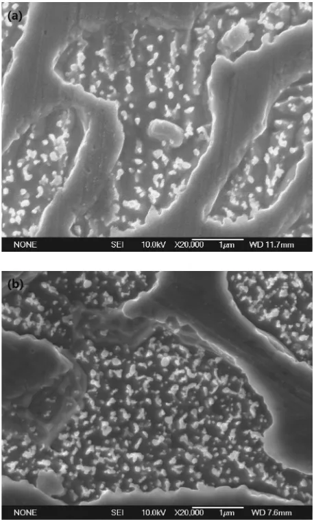
Figure 4 shows the microstructures of the Sn-58Bi solder joint and the composite solder joint. The features observed are quite typical of a eutectic Sn-58Bi solder and consist of fine alternating lamellae of two constituent phases. From Fig. 4(a) and (b), it can be seen that the addition of a small amount of Sn-3.0Ag-0.5Cu nanoparticles to the eutectic Sn-58Bi solder marginally altered the as-solidified micro-structure. Compared with the pure eutectic solder, the addition of nanoparticles is favorable to form a large number of nanosized grain with uniform distribution. It indicates that the dispersed nanoparticles will result in grain refining. One possible explanation is that the Sn-3.0Ag-0.5Cu nanoparti-cles dispersed throughout the composite microstructure, obstructing movement of dislocation and pin grain bounda-ries, and result in dispersion-strengthening.7,15)
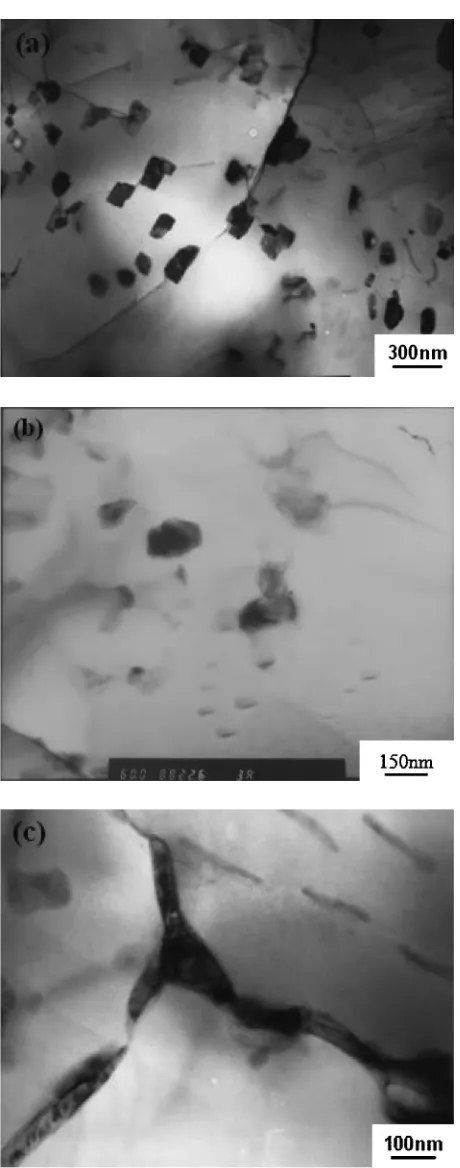
The morphology of composite solder was also observed by TEM as shown in Fig. 5. From Fig. 5(a), it can be seen that the nanoparticles generally distributed uniformly. Mean-while, we can see that there was a little variation in the shape of nanoparticles, which may be due to the possible surface melting of under-melting point (pre-melting) of nanoparticles and re-crystallize during the reflow process. Although a small amount of nanoparticles were agglomerated, the reunited
gobbets contained only several nanoparticles, as shown in Fig. 5(b). From Fig. 5(c) we can see that the nanoparticles were easily located in crystal grain boundaries or near the grain boundaries. Because of these gathered particles, the crystal grain boundaries would be pinned. The TEM observation would be helpful to understand the fact that the crystal grains were refined with nanoparticle addition to the eutectic solder. A more detailed analysis of the micro-structure of composite solder joint can be also found in our
recent work.16) However, the behavior of Sn-3.5Ag-0.5Cu
nanoparticles in the reflow process of composite solder paste will be studied further in detail.
Figure 6 shows the diffraction patterns of nanoparticles in the Fig. 5(a). The diffraction patterns indicated the formation
of Ag3Sn and Cu6Sn5, and further proved that Sn-Ag-Cu
nanoparticles have actually dispersed into the solder matrix and still exist after reflow soldering process.
3.3 Contact resistance
The variation of average contact resistance of the solder joints during thermal cycling is presented in Fig. 7. For all solder joints, the contact resistance exhibited was quite stable in the range of 0, 260, 320, 380, 440 and 500 cycles. The Fig. 3 DSC curve of composite solder joint with 3 mass% Sn-3.0Ag-0.5Cu
nanoparticles at heating rate of 5C/min.
[image:3.595.53.286.71.244.2] [image:3.595.312.541.72.451.2]percentage change of the contact resistance of solder joints is less than 10% after 500 cycles. So, all kinds of sample can pass through 500 thermal cycling without electrical failure.
3.4 Shear strength
Figure 8 shows the average shear strength and standard deviation for composite solder joints with two kinds of pure
eutectic solders. The values of average and standard devia-tion obtained from 40 sheared solder joints for every case of all 12 cases is shown in Table 1. From Fig. 8, before thermal cycling, the average shear strength of all composite solders was above 30 MPa. These values were 2 times higher than the 15 MPa of Sn-58Bi and close to the average shear strength of Sn-3.0Ag-0.5Cu. The enhancement of shear strength of composite solder could be attributed to finer crystal grains from the addition of nanoparticles in solder matrix. The fine Fig. 5 TEM images of composite solder joint: (a) Nanoparticles distributed
in composite solder joint (b) Small amount of agglomerated nanoparticles (c) Nanoparticles and crystal grain boundaries.
Fig. 6 Electron diffraction patterns of nanoparticles: (a) Ag3Sn (b) Cu6Sn5.
[image:4.595.55.285.64.648.2] [image:4.595.312.542.73.431.2] [image:4.595.317.535.475.648.2]grains reduced dislocation movement near the grain bounda-ries, since, with the nanoparticles, much more energy was needed for the dislocation movement to travel across the boundaries.5)
From Fig. 8, we can also see that after 500 cycles of thermal cycling, the average shear strengths of composite solder were lower than those before thermal cycling. The average strength decreased monotonically with the increas-ing of weight percentage of nanoparticles. The decrease in average shear strength after thermal cycling was 1.5% to 3.5% when the weight percentage of nanoparticles was lower than 2 mass%. However, the average shear strength of composite solder after thermal cycling sharply decreased by about 15% when the weight percentage of nano-particles reached 3 mass%. In addition, the shear strength of pure eutectic Sn-58Bi and Sn-3.0Ag-0.5Cu also decreased by 23.5% and 6.5% respectively after thermal cycling Meanwhile, from Fig. 8, all samples showed the standard deviation to remain nearly at a constant level.
It is known that grain boundary sliding is the predominant mode of TMF damage that occurs during the high-temper-ature dwell in a TMF cycle.5)The results of the shear strength tests after thermal cycling indicated clearly that TMF resistance of the composite solder with 1 mass% nano-particles increased 16 times in comparison to Sn-58Bi and 4 times in comparison to Sn-3.0Ag-0.5Cu. In the present test, the grain boundary slide could be constrained effectively during thermal cycling due to the nanoparticles in grain boundaries, as mentioned above. However, adding too much nanoparticles resulted in a degradation of shear strength. This result indicated that on one side the addition of nanoparticles would be helpful to refine the crystal grain, but on the other side the addition of nanoparticles could easy to cause the initiation and propagation of micro-cracks at the interfaces between the unmelted nanoparticles and the solder matrix during thermal cycling.
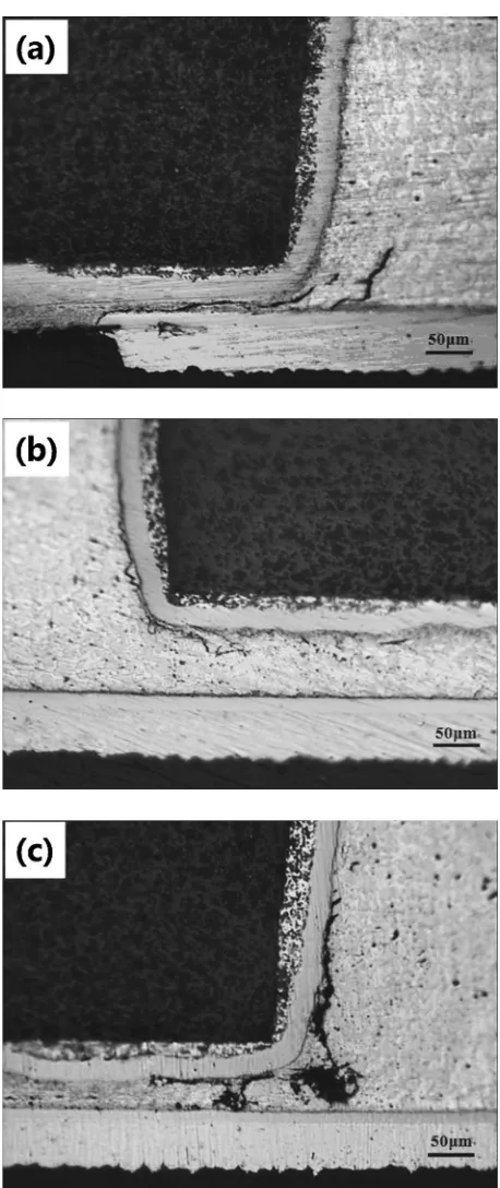
A cross-section inspection was made to detect any crack initiation and propagation in the solder matrix after the thermal cycling. The fatigue cracks in Sn-58Bi and compo-site solders with 3 mass% and 4 mass% nanoparticles are
shown in Fig. 9. In the cases of Sn-3.0Ag-0.5Cu and composite solders with 1 mass% and 2 mass% nanoparticles, no crack was found after 500 cycles of thermal cycling. The results of cross-section corresponded well with the data of shear strength, indicating that the initiation and propagation of cracks in solder joints after thermal cycling resulted in the decrease of shear strength, though these cracks have not developed enough to cause obvious change of contact resistance yet during thermal cycling.
Fig. 8 Average and standard deviation (STDEV) of shear strength of composite solder with two conventional eutectic solders before and after thermal cycling.
[image:5.595.312.541.66.610.2] [image:5.595.60.278.69.248.2]3.5 Fracture mode
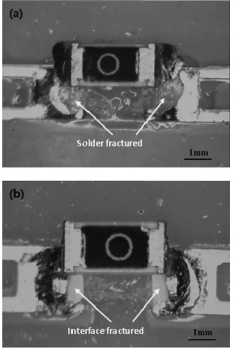
All samples were inspected under OM after the shear test to identify the fracture mode. From inspections, two kinds of fracture modes were found. The first kind was a fracture located within the solder itself, as shown in Fig. 10(a). The second kind was a fracture located at the interface between solder joint and resistor ends, as shown in Fig. 10(b). In order to clearly show the fracture location, the chip resistors are also included in the pictures.
Two fracture modes, fracture within solder and fracture at interface, were counted respectively. Figure 11 shows the percentages of two fracture modes which were calculated from 40 sheared solder joints of every case.
From Fig. 11, before thermal cycling, the fracture within solder was only observed for pure Sn-58Bi case, because the Sn-58Bi solder was often brittle.17)After 500 thermal cycles,
the fracture within solder was observed for pure Sn-58Bi and all reinforced composite solder cases. For pure Sn-58Bi case, the percentage of fractures within the solder increased by 30%. For reinforced composite solder case, the percentage of fractures within solder was less than that for Sn-58Bi case, but increased monotonically with the weight percentage of nanoparticles.
In general, after thermal cycling, the percentage of fractures within solder was just 5% in composite solder with 1 mass% and 2 mass% nanoparticles. Meanwhile, 82.5%
fracture within solder was present for pure Sn-58Bi. It can be concluded that the composite solder is 16 times stronger in terms of TMF resistance when nanoparticles were mixed into the solder matrix up to 2 mass%. However, the fractures within solder were detected largely in composite solders with 3 mass% and 4 mass% nanoparticles after thermal cycling. The percentages of fractures within solder increased by 22% and 45% respectively for composite solder with 3 mass% and 4 mass% content of nanoparticles. This indicated that the tendency for forming micro-cracks between nanoparticles and solder matrix was increased when nanoparticles ex-ceeded 3 mass% in solder joint.
4. Conclusions
In this work, a reinforced composite solder with low melting point was developed and investigated. The compo-site solder was prepared by adding Sn-3.0Ag-0.5Cu nano-particles into a conventional 58Bi solder paste. The Sn-3.0Ag-0.5Cu nanoparticles were manufactured with self-developed CDCA technology.
The melting peaks of Sn-58Bi and Sn-3.0Ag-0.5Cu were both observed from the DSC scanning profile. It shows that Sn-3.0Ag-0.5Cu nanoparticles are present in the composite solder joint after the reflow process.
The results from SEM observations showed the crystal grains were refined with the addition of nanoparticles to the eutectic solder. The TEM observations indicated that distribution of nanoparticles was generally uniform, and nanoparticles were easy to locate in crystal grain boundaries or near grain boundaries. The measurement data of solder joint contact resistance showed that after 500 thermal cycles, the variation of contact resistance was less than 10% without electrical failure.
[image:6.595.53.285.73.421.2]Shear strength of the composite solders with different weight percentages of nanoparticles was studied before and after thermal cycling, and compared to pure eutectic Sn-58Bi and Sn-3.0Ag-0.5Cu solder. Before thermal cycling, the average shear strengths of all composite solders were above 30 MPa, which was far higher than that of Sn-58Bi (15 MPa) and near the average shear strength of Sn-3.0Ag-0.5Cu. After the thermal cycling, the average shear strengths of Fig. 10 Fracture surface observations after shear testing: (a) Fracture in
solder (b) Fracture at interface.
[image:6.595.317.535.73.248.2]of fractures within solder was less than that of Sn-58Bi, but increased monotonically with the weight percentage of nanoparticles. As with the shear test results, when con-tent of nanoparticles increased from 2 to 3 mass%, the percentage of fractures within solder sharply increased from 5 to 22%.
The results detailed in this work indicate that the composite solder became stronger when a certain amount of nanoparticles was added into the solder matrix. However, after thermal cycling, the tendency of forming micro-cracks between nanoparticles and solder matrix and fracture within solder was increased when the nanoparticle content exceeded 3 mass%.
Acknowledgement
We acknowledge the financial support from the Chinese Ministry of Science and Technology (2008AA04Z301), from 863 program on nanosolder paste (2006AA03Z339) and from Shanghai Municipal Education Commission (No. 07ZZ15). This work is also supported by the EU FP7 IP Nanopack program and from the Swedish National Science Foundation under the project ‘‘Nanointerconnect’’ (621-2007-4660).
5) A. Lee and K. N. Subramanian: Electron. Mater.34(2005) 1399–1407. 6) Y. S. Shin, S. H. Lee, C. W. Lee, S. B. Jung and J. H. Kim: Proc. 10th IEEE CPMT Conf. on Electronics Packaging Technology, (2008) pp. 279–284.
7) D. C. Lin, S. Liu, T. M. Guo, G. X. Wang, T. S. Srivatsan and M. Petraoli: Mater. Sci. Eng. A360(2003) 285–292.
8) X. Z. Xia, C. D. Zou, Y. L. Gao, J. Liu and Q. J. Zhai: Proc. IEEE CPMT Int. Symp. on High Density Packaging and Microsystem Integration, (2007) pp. 302–304.
9) W. B. Guan, S. G. Verma, Y. L. Gao, C. Anderson, Q. J. Zhai and J. Liu: Proc. 1st IEEE CPMT Conf. on Electronics System Integration Technology, (2006) pp. 7–12.
10) J. Liu, C. Anderson, Y. L. Gao and Q. J. Zhai: Proc. 10th IEEE CPMT Conf. on Electronics Packaging Technology, (2008) pp. 84–93. 11) F. Stepniak: Microelectron. Reli.44(2004) 805–814.
12) C. D. Zou, Y. L. Gao, B. Yang, Q. J. Zhai, C. Andersson and J. Liu: Solder. Surf. Mount Technol.21(2009) 9–13.
13) H. J. Jiang, K. S. Moon, H. Dong, F. Hua and C. P. Wong: Chem. Phys. Lett.429(2006) 492–496.
14) H. J. Jiang, K. S. Moon, F. Hua and C. P. Wong: Chem. Mater.19
(2007) 4482–4485.
15) D. C. Lin, G. X. Wang, T. S. Srivatsan, M. A. Hajri and M. Petraroli: Mater. Lett.57(2003) 3193–3198.
16) L. L. Zhang, W. K. Tao, J. Liu, Y. Zhang, Z. N. Cheng, C. Anderson, Y. L. Gao and Q. J. Zhai: Proc. IEEE CPMT Int. Conf. on Electronics Packaging Technology and High Density Packaging, (2008) p. 167. 17) S. Kikuchi, M. Nishimura, K. Suetsugu and T. Ikari: Mater. Sci. Eng. A