Modular Multilevel Converter Grid-Interface for
Klystron Modulators: an Augmented Modulation
Scheme for Arm Balancing
Marija Jankovic
∗, Alessandro Costabeber
∗, Alan Watson
∗, Jon Clare
∗and Davide Aguglia
∗∗ ∗University of Nottingham, Nottingham, NG7 2RD, UK
∗∗
CERN-European Organization for Nuclear Research, Geneva, CH-1211, Switzerland
Abstract—This paper discusses the control of a Modular Multilevel Converter (MMC) used as a grid-interface for the klystron modulators in the Compact Linear Collider (CLIC). The converter has a DC side load which takes short-duration power pulses, causing high DC side power fluctuations that are not tolerable if seen by the AC grid. The DC-AC power decoupling capability of the MMC enables mitigation of the power ripple on the AC side, guaranteeing compliance with power quality requirements. However, the pulse repetition rate of the CLIC modulators is synchronised the the 50HzAC grid and this induces permanent power imbalance in the arms of the MMC, causing voltage deviation and over-modulation unless appropriate balancing strategies are implemented. Unlike existing arm balancing methods that control 50Hzcirculating currents to balance the arm powers, the method proposed in this paper introduces an augmented modulation strategy where modulation signals are redistributed among arms based on the demand from a balancing controller. The resulting controller has lower complexity and its simple structure enables an easier design of the balancing loop, which guarantees predictable dynamics in operation. The effectiveness of the method has been demonstrated in simulation for the full scale CLIC converter ratings and experimentally on a 7kW MMC prototype operating with a 3.3kApulsed DC load.
Index Terms—Arm balancing control, Grid-connected con-verter, Pulsed Power, Modular Multilevel Concon-verter, Modulation strategy, Klystron Modulator
I. INTRODUCTION
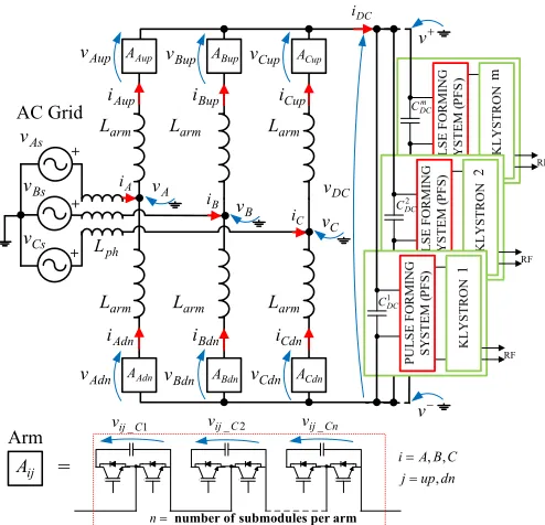
Future high-luminosity colliders, such as the Compact Lin-ear Collider (CLIC), require input power supplied to the accelerating cavities via high voltage, high power pulses. Klystron modulators, in the case of CLIC, draw short duration high current pulses with a repetition frequency of 50Hzfrom a medium voltage DC source, to produce high voltage pulses at the klystrons [1]. The power electronic grid-interface for the klystron modulators has to be highly efficient and reliable, capable of processing high powers and must be able to prevent propagation of the pulsed power effects from the DC side to the AC grid [1], [2]. The Modular Multilevel Converter (MMC) shown in Figure 1 has been selected as a suitable topology [3] due to its modularity, efficiency and high quality AC waveforms [4]. Additionally, the independent control of AC and DC side currents [5] enables cancellation of the DC side power pulsation from the AC grid.
Unlike typical HVDC/MVDC applications, where the MMC operates without a bulk DC capacitor, in the application of interest the MMC operates with a DC link comprising the capacitor banks of the klystron modulators, as shown in Figure 2. These are periodically discharged by the high current
RF
RF
arm
L
arm
L
arm
L
arm
L
arm
L
arm
L
RF
= +
+
+
1 DC C
2 DC C
1
2
m
Aup
v vBup vCup
Cdn
v
Bdn
v
Adn
v
DC
v
ph
L
DC
i
Aup
i
Adn
i iBdn
Bup
i
Cdn
i
Cup
i
As
v
Bs
v
Cs
v
A
v
B
v
C
v
C
i
B
i
A
i
m DC C
1 _C ij
v vij_C2 vij_Cn
dn up j
C B A i
, , ,
arm per submodules of number n Aup
A ABup ACup
Cdn
A
Bdn
A Adn A AC Grid
ij A Arm
v
[image:1.612.314.561.198.436.2]v
Fig. 1.Three phase Modular Multilevel Converter grid-interface for klystron modulators.
DC
i
DC v
pulse i
DC
C
t
ms
20 pulse i
DC v
t
Fig. 2.Lumped equivalent circuit of the klystron modulators.
pulses, with a duration of approximately 140µs, drawn by the modulators. In between pulses, the grid-interface converter draws power from the AC grid to restore the voltage on the capacitor bank. For CLIC, the capacitors are designed to limit the droop to 10% of the nominal DC voltage. The main challenge for the grid-side converter and its control is to ensure an AC power fluctuation below 2% [1], [2]. The nominal converter and klystron modulator ratings, obtained by system optimisation studies [3], are summarised in Table I. The MMC parameter design is based on [6].
[image:1.612.368.509.470.543.2]bandwidth current control is used in each modulator to min-imise the voltage ripple seen by the grid-interface. However, taking advantage of the internal energy storage, an MMC can generate the required AC currents despite large DC power fluctuations, thus minimising the AC power fluctuation with a single converter stage that does not affect cost and complexity of the modulators and does not require time critical controllers [8].
Unfortunately however, the DC current pulse repetition rate in this application matches the AC grid frequency and as a result it introduces a constant source of imbalance between the cell capacitor voltages of the upper and lower MMC arms [9], [10]. This leads to overmodulation and distortion of the AC power [11] unless adequate balancing controllers are implemented. Various different arm balancing methods have been reported so far in the literature, and they can be classified as those acting on the specific cell modulation signal to guarantee correct cell capacitor voltage [12]–[14] and others manipulating the circulating current reference [15], [16]. These methods are aimed at compensating for small converter asymmetries due to non-idealities of the converter and transient imbalances. As a result, the dynamics of the small correction terms are not significant for the overall converter operation, provided that stability is ensured. For this reason, balancing controller design is not typically studied in detail in the literature.
A preliminary arm balancing method for the CLIC grid-interface MMC was proposed by the authors in [10]. The method was based on the addition of a 50Hz component to the circulating current in quadrature with the 50Hzcomponent of the DC voltage ripple. The main drawback of the solution was its sensitivity to the position of each pulse within the AC voltage period, with some critical positions were arm balanc-ing was not possible, resultbalanc-ing in high AC power fluctuation. Therefore, the method would require the klystron modulators to be phase-locked with the grid, to guarantee that the pulses does not occur in the non-controllable regions. The solution in [10] belongs to the arm balancing methods manipulating the circulating current reference, and like other similar methods it requires the generation of an AC circulating current reference and the implementation of suitable controllers, for example Proportional-Integral (PI) or Proportional-Resonant (PR) [17], to track it.
A preliminary analysis of the new method proposed in this paper was first presented in [9]. However, only the basic concept was discussed and validated in steady state operation. No in-depth analysis of the balancing control design and of the interactions with the other controllers of the MMC was provided. The aim of this paper is to fill that gap, providing a comprehensive analysis and design of the proposed balancing controller, validated by a set of experimental results on a 7kW
MMC lab demonstrator with a 3.3kA, 150µs pulsed load emulator.
[image:2.612.342.531.64.190.2]The paper is organised as follows. In Section II, MMC operation is briefly reviewed. Section III provides an analysis of the arm power imbalance caused by the pulsed DC load. Sections IV and V discuss the new arm balancing control algo-rithm based on the augmented modulation scheme, providing a
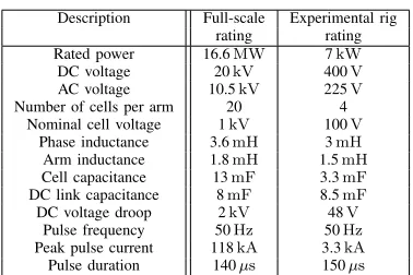
TABLE I.Converter and load parameters.
Description Full-scale Experimental rig rating rating Rated power 16.6MW 7kW
DC voltage 20kV 400V
AC voltage 10.5kV 225V
Number of cells per arm 20 4 Nominal cell voltage 1kV 100V
Phase inductance 3.6mH 3mH
Arm inductance 1.8mH 1.5mH
Cell capacitance 13mF 3.3mF
DC link capacitance 8mF 8.5mF
DC voltage droop 2kV 48V
Pulse frequency 50Hz 50Hz
Peak pulse current 118kA 3.3kA
Pulse duration 140µs 150µs
detailed analysis of the controller design and of its interaction with the existing circulating current controller. Section VI presents results from a simulation study in PLECS to validate the proposed arm balancing method and its performance on the full-scale grid-interface MMC for the CLIC (Table I). Finally, in Section VII the proposed method is experimentally validated on a laboratory-scale prototype (Table I) and Section VIII gives the conclusions of the work.
Remark:throughout the paper, equations are given only for phase A of the converter for brevity.
II. MMCGRID-INTERFACE BASIC OPERATION AND CONTROL ARCHITECTURE
The arrangement of an MMC grid-interface feeding a set ofm klystron modulators is shown in Figure 1. Table I gives the total average powers and the peak pulsed current drawn by the Pulse Forming Systems (PFSs) in the full power CLIC converter and in the laboratory scale demonstrator. From the different possible arrangements for the real application [18], the arrangement and ratings considered here are m = 82
synchronised klystrons per MMC, each rated for 29M W
pulsed power, for a total of 2.37GW. The pulse duration is 140µs, giving an average power of 16.6M W if the pulse repetition frequency is 50Hz. As a result, each power pulse corresponds to a current pulse of118kAdrawn from the total equivalent DC link capacitor CDC. For the purpose of the
analysis in this section and the following one, the lumped circuit in Figure 2 will be assumed where all the klystrons and the PFSs are modelled as a DC link capacitance CDC
in parallel with a current source drawing current pulses. The same lumped representation has been adopted in the design of the experimental rig.
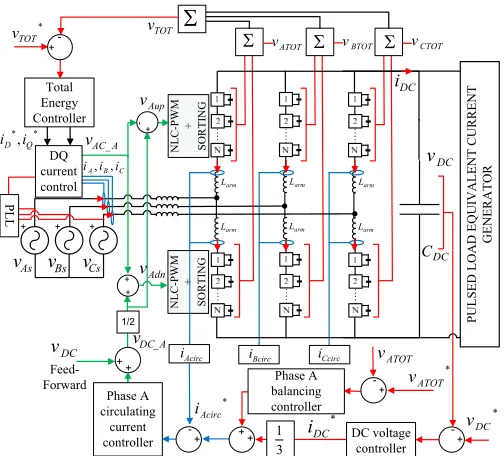
In the following paragraphs, a review of the MMC [4] operating principle and control is briefly presented. As shown in Figure 1, each phase has two sets of controllable chains of half bridge submodules with floating capacitors (upper and lower arm) and two arm inductors. The AC side equation for phase A can be written as:
vAs−Leq
diA
dt +
vAup−vAdn
2 =
v++v−
2 , (1)
where Leq = Lph + Larm2 is the equivalent AC circuit
(vAup) and the lower (vAdn) arms in each phase as shown
in Figure 3. The AC current references are driven by the total energy controller, which guarantees that the sum of all the submodule capacitor voltages vT OT is maintained at the
nominal value by adjusting the power absorbed from the AC grid. The relationship between the AC voltage demand and the upper and lower arm modulation signals can be written for phase A as:
vAC A=−
vAup−vAdn
2 , (2)
where the converter arms are assumed to be ideal controlled voltage sources, imposing the voltage demand of the current controller, i.e. the NLC-PWM and cell sorting blocks [20], [21] in Figure 3 are neglected for simplicity. A second equation can be written for the DC side of the converter:
vAup+vAdn−2Larm
diAcirc
dt =v
+−v−=v
DC, (3)
whereiAcirc is the circulating current of phase A, defined
as:
iAcirc=
iAup+iAdn
2 . (4)
From the DC side equation, it can be seen that the circulat-ing current can be controlled by actcirculat-ing on the control variable:
vDC A=vAup+vAdn. (5)
In the CLIC, the MMC must control the voltage across
CDC, recharging it after each load pulse, as indicated in
the overall control scheme shown in Figure 3. An average DC voltage controller can be implemented by generating a reference for iDC which is then divided into three identical
circulating current references for the three phases. The low frequency circulating currents are controlled by Proportional-Integral (PI) controllers. The circulating current references are then corrected with a small DC component generated by a phase balancing controller, that ensures equal energy redistribution among phases [10]. It should be noted that this simplified analysis is true under the assumption that the arms can be treated as ideal voltage sources, and neglecting the impact of the second harmonic circulating currents [11], [19]. The modulation demands for the upper and lower arms of phase A can be described by equation Eq. (6) by combining the demands from the AC and DC side controllers:
vAup=
vDC A
2 −vAC A, vAdn=
vDC A
2 +vAC A. (6)
III. PULSED LOAD EFFECTS
With a non-pulsed load, the AC and DC controllers dis-cussed in the previous section will enable correct operation of the converter. However, in the application under study the DC voltage has a 50Hzripple due to the klystron pulse repetition frequency. In the controller in Figure 3, the DC voltage ripple will be transferred to the upper and lower arm voltages Eq. (6) by the action of the circulating current controller, and will interact with the 50Hzcomponents of the arm currents:
iAup =iAcirc+
iA
2 , iAdn=iAcirc− iA 2 (7) arm L arm L arm L arm L arm L arm L + + + arm L arm L
Bcirci iCcirc
Acirc i
DC
v
ATOT
v vBTOT vCTOT
* DC v N L C -P W M + S O R T IN G C B A i i i, ,
As v * TOT v * *, Q D i i + -* DC i * Acirc i + - vATOT*
ATOT v + -Phase A balancing controller N L C -P W M + S O R T IN G Bs v P U L S E D L O A D E Q U IV A L E N T C U R R E N T G E N E R A T O R Cs v P L L 1/2 DC i 3
1 DC voltage
[image:3.612.313.565.55.283.2]controller Phase A circulating current controller Total Energy Controller + + DC v Feed-Forward DQ current control A DC v _ A AC v _ Aup v Adn v TOT v N 2 1 N 2 1 arm L arm L + + DC C
Fig. 3. Architecture of the DC side and AC side controls of the MMC grid-interface for klystron modulators - all controllers are Proportional-Integral (PI).
to produce a non-zero average power with opposite signs in the arms of each phase. This causes divergence of the cell capac-itor voltages, even if capaccapac-itor voltages are perfectly balanced within each arm and the converter operates in global power balance. As a consequence, overmodulation will ultimately occur, leading to AC power distortion [10].
If the modulation strategy follows the conventional one given by (6), arm balancing can be achieved by acting on the circulating current reference in each phase through an additional AC component coming from an arm balancing controller. Such an arm balancing controller would generate an AC circulating current reference according to existing balancing techniques [10], [16]. Alternatively, as proposed here, arm balancing can be achieved by redistributing the arm voltage references among the arms, without an explicit generation of a balancing circulating current component, thus simplifying the control structure.
IV. PROPOSED AUGMENTED MODULATION SCHEME
The method proposed in this paper achieves arm balancing by tailoring the distribution of the AC modulation signals between the arms within each phase according to balancing requirements. Based on Eq. (2), the modulation signals can be redistributed among the arms without affecting the AC component of the voltage reference or the AC grid current [9]. The distribution of the DC voltage reference should remain unchanged, to avoid DC components in the converter AC voltages. This can be achieved by using equations Eq. (8) instead of equation Eq. (6) in the repartition of the modulation signals, i.e.:
vAup=vDC A
2 −(1 +xA)vAC A,
and
vAdn=
vDC A
2 + (1−xA)vAC A,
∑
= n kCk Aup v n 1.. _ 1
∑
= n kCk Adn v n 1.. _ 1
н
н н
Ͳ
йy
A
x
AVG 20ms
AVG 20ms
p x
k_
i x
k _ s 1
+ +
[image:4.612.59.289.57.107.2]PI based controller
Fig. 4. ParameterxAgeneration on the basis of the normalised cell capacitor voltages imbalance on the example of phase A.
+
−
+ − + −
+
−
+ − + −
vDC vAC_A
iA
iAup
iAdn Larm
Larm Lph
vAs
xAvAC_A
vDC_A 2
vAC_A xAvAC_A
vDC_A 2
Fig. 5.Simplified schematics of the phase A of an MMC with uneven distribution of AC voltage reference.
where xA controls the distribution of the AC modulation
signal. The basic principle is that the redistribution of the AC modulation signals between the upper and lower arms induces another source of arm imbalance, independent from the pulsed DC load effect. This can be controlled by xi, i = A, B, C,
in each phase to counteract the effect of the pulses and re-establish arm balancing. In steady state, thexi have constant
values defined by the Proportional-Integral (PI) controllers that regulate the arm imbalance to zero in each phase as shown in Figure 4 for phase A.
The simplified converter diagram for phase A is given in Figure 5, where it can be seen that xAvAC A only affects
the DC side equivalent circuit and not the AC side equivalent circuit [22]. This confirms that the proposed method will not cause uneven distribution of the AC current between arms. A non-zero xA generates a 50Hz voltage in the differential
circuit that drives a 50Hzcomponent in the circulating current. The interaction of this current with the AC components of the arm voltages gives a power contribution that can be used to counteract the effect of the pulsed load, as discussed in detail in the following section. The 50Hzcurrent is seen as a disturbance by the circulating current controller whose effect on the arm balancing controller must be carefully taken into account in the analysis and design of the proposed balancing method.
p circ
k _
i circ
k _ s
1
DC v
ref A DC
v _
+
+ ++
+- +-- 2Larms
1 A
AC Av
x _
2
Acirc i ref Acirc
i iAcirc
[image:4.612.51.294.166.273.2]PI based controller plant
Fig. 6.Closed loop circulating current controller with arm balancing control acting as a disturbance.
V. AUGMENTED MODULATION SCHEME AND ARM BALANCING CONTROL DESIGN
Remark:In this section, design of the Proportional-Integral controllers will be based on the Bode design approach [17], where target Phase Margin (PM) and Bandwidth are defined and the proportional and integral gain derived analytically using the model of the control plant. It is important to note that the choice of target Phase Margin and Bandwidth is not unique. Both Bandwidth and Phase Margin are typically maximised within the constraints imposed by the modelling method used to derive the control plant and by the restrictions imposed by nested control structures. Referring to Phase Margin, PM>60◦ is usually desirable to guarantee damped response and robustness to changes in the system parameters. The closed loop circulating current controller diagram is illustrated for phase A in Figure 6. The plant model is based on the DC side equation and the arm balancing controller acts as a disturbance through the component2xAvAC A. Since the
circulating current now has a 50Hzcomponent, the circulating current controller will have non-zero error under steady state conditions, with the mean value following the reference. Thus, the output of the DC side controller including DC voltage feed-forward and the Proportional-Integral (PI) controller output, is a function of the circulating current 50Hzcomponent and can be approximated as:
vDC A=vDC+vDC A0−kcirc p·iAcirc50
−kcirc i Z t
0
iAcirc50(τ)dτ,
(9)
where vDC A0 is a DC offset ensuring that the mean
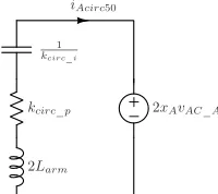
circulating current follows its constant reference. From Eq. (9) and the equivalent circuit in Figure 5, the differential circuit can be represented as a series connection of a resistorkcirc p
and a capacitor 1/kcirc i at 50Hz, as shown in Figure 7.
The relationship between the circulating current 50Hz com-ponent and the converter AC voltage can be written as:
IAcirc50=−
2xAVm
Zarm
φAcirc50=φvA−∆φcirc50, (10)
whereIAcirc50andφAcirc50are the amplitude and phase of the 50Hz component of the circulating current,Vm andφvA are
the amplitude and phase of the phase A AC voltage reference andZarm and ∆φcirc50 are the magnitude and phase of the equivalent RLC impedance in Figure 7 at 50Hz(assumed to be the same in all the three phases).
+ −
iAcirc50
2Larm
kcirc_p 1
kcirc_i
[image:4.612.414.514.636.725.2]2xAvAC_A
[image:4.612.51.295.670.735.2]Combining Eqs. (9) and (10), neglecting all the DC com-ponents and defining vDC50 as the 50Hz fundamental of the DC voltage ripple caused by the pulsed load and vDC A50 as the 50Hzcomponent in Eq. (9), the 50Hzupper arm voltage and current can be derived as:
vAup50= vDC A50
2 −xAvAC A−vAC A
= vDC50
2 +Larm
diAcirc50
dt −vAC A,
(11)
and
iAup50=iAcirc50+iA
2 . (12)
The lower arm voltage and current can be derived in a similar manner. The average power of the upper and lower arms can be derived and their difference ∆PAarm can be written as:
∆PAarm=−VDC50Imcos(4φDC50−φAi)
+xALarmωVmImcos(φvA−∆φcirc50+π2−φiA) Zarm
−2xAVm2cos(∆φcirc50)
Zarm =−N U MA+xADEN,
(13)
where VDC50 and φDC50 are the amplitude and phase of
vDC50andImandφAiare the phase A AC current amplitude
and angle. An analytical estimation of the steady-state value of xA required to balance the arms of an MMC feeding the
pulsed DC load can be derived setting Eq. (13) to zero:
xA= N U MDENA. (14)
The value N U MA depends on the pulsed DC load and on
the AC current while DEN depends on the AC current and voltage and on the circulating current controller parameters through Zarm and ∆φcirc50. Assuming balanced grid
condi-tions,DEN is the same for all the three phases. The relation between the power difference ∆PAarm and the difference of
the sums of cell capacitor voltages ∆vAarm in the upper and
lower arms is given by:
∆PAarm= Ccell
·VDC
n
d∆vAarm(t)
dt . (15)
Therefore, the Proportional-Integral (PI) arm balancing con-troller in Figure 4 can be represented in more detail in Figure 8, where the term1/(2VDC)represents a normalisation by the
sum of all the nominal cell voltages and the measured voltages
∆vAarm are averaged over (20ms) to filter the ripple.
The pulsed DC load, which is the source of imbalance, acts as a disturbance to the arm balancing controller through
N U MA and therefore the balancing control design will be
independent from the specific value of imbalance. This is a
DC V
2
1 PI
S/H 20ms sCcell VDC n
A
x
n k
Ck Adn n
k Ck Aup
Aarm v v
v
.. 1
_ ..
1 _
DEN A NUM
+
-Fig. 8.Closed loop representation of the arm balancing controller for phase A.
1000 3000
5000 20 40
60 −50
0
kcirc p[V/A]
kcirc i[V/As]
D
E
N
[k
W
]
1000 3000
5000 20 40
60 −1.5
−1 −0.5 0 0.5
kcirc p[V/A]
kcirc i[V/As]
∆
φci
r
c
5
0
[r
a
d
[image:5.612.315.560.59.139.2]]
Fig. 9.DENand the phase shift∆φcirc50vs. the circulating current Proportional-Integral (PI) controller gains.
desirable feature since load pulses can occur with different phase with respect to the grid voltages, leading to different imbalances in the different phases as shown in Eq. (13). Referring to the full-scale CLIC converter in Table I, the circu-lating current controller in Figure 6 has been initially designed for a nominal bandwidth of 3750rad/s and phase margin (PM) of 89◦, which corresponds toknom
circ p = 13.3 V/A and
knomcirc i= 532 V/A/s.
To evaluate the impact of the circulating current controller design on the proposed arm balancing method,DEN and the phase shift∆φcirc50Eq. (10) (both functions of the circulating current controller) are computed for different current controller parameters as shown in Figure 9. The proportional gain is in a range of (k
nom circ p
5 ,5kcirc pnom ) and the integral gain is in a range
of (kcirc inom
10 ,10k
nom
circ i). For bothDEN and∆φcirc50, the lines ofknom
circ p andkcirc inom are shown in red and blue, respectively.
The red line corresponds to nearly constant bandwidth while the PM is varied. The blue line corresponds to change of both bandwidth and PM. When the circulating current controllers have high bandwidth and high PM, the proposed balancing scheme produces a circulating current almost aligned with the AC voltage vector, showing the affinity between this method and the methods introduced in [15] and [16]. However, the value of DEN approaches zero, requiring a larger xA
to achieve balancing. Conversely, low bandwidth circulating current controllers lead to a larger phase shift between the AC voltage and circulating current and a larger absolute value of DEN. Therefore, a trade-off between circulating current control bandwidth and balancing is needed.
[image:5.612.57.300.120.213.2]For the CLIC parameters in Table I, the nominal design for the circulating current controller is considered acceptable given the relatively high bandwidth and the value ofDEN in Figure 9. Therefore, the arm balancing controller in Figure 8 assumesknom
circ p andkcirc inom and has been designed to achieve
a bandwidth of 7rad/sand a PM of 65◦, yieldingkx p= 0.3
andkx i= 1 s−1.
VI. SIMULATION RESULTS
The MMC grid-interface for the CLIC with the proposed arm balancing controller has been simulated in PLECS initially according to the full-power ratings in Table I. The sampling frequency and equivalent switching frequency is 10kHz. The control gains used in the simulation are given in Table II and refer to the continuous-time control schemes shown in Figs. 3-8.
[image:5.612.62.281.667.733.2]Controller Proportional Integral Bandwidth Phase Current kdq p 9 kdq i 900 2000 [rad/s]
Circ. Current kcirc p 13.3 kcirc i 532 3750 [rad/s]
Energy ken p 140 ken i 70 10 [rad/s]
DC voltage kdc p 0.083 kdc i 0.83 12.5 [rad/s]
Ph. balancing kpb p 0.014 kdc i 0.007 20 [rad/s]
Arm balancing kx p 0.3 kx i 1 7 [rad/s]
Without loss of generality, results are shown for a pulse position of 0.534rad with respect to the phase A positive zero crossing. Figure 10 presents the converter waveforms in steady state. From top to bottom, the converter phase currents and voltages and the DC current and voltage are presented
(vXs and iX with X = A, B, C, vDC and iDC in Figure
1). The 50Hz component is present in the DC current, as a consequence of the 50Hzcomponents in the three circulating currents, caused by the arm balancing controllers. A variation of the pulse position affects the amount of disturbance in each phase, i.e.N U MA,B,Cis different, leading to differentxA,B,C
values and different amplitudes of the 50Hzcomponent in the circulating current.
Figure 11 shows the converter AC and DC side instanta-neous powers where it can be seen that the AC power ripple is very low, below 0.3%despite the large DC power fluctuation caused by the pulsed load.
Finally, to validate the dependence of the steady state values of xA,B,C and IA,B,Ccirc50 on the design of the circulating current control, simulations have been run for five pairs of cir-culating controller gains: (kcirc p,kcirc i), (kcirc p,10kcirc i),
(kcirc p, kcirc i10 ), (5kcirc p,kcirc i) and (kcirc p10 , kcirc i). The
values obtained for xA,B,C and IA,B,Ccirc50 are shown in Figure 12. In accordance with the analysis in Section V, the circulating current amplitudes are comparable for all the cases except the second, that corresponds to a larger absolute
∆φcirc50value in Figure 9. Moreover,xA,B,C increase when
the bandwidth of the circulating current controller increases causing a smaller absolute value of the DEN in Figure 9.
The full-scale simulation results confirm the feasibility of the arm balancing method and demonstrate the impact of the circulating current control design for the operation of an MMC as a grid-interface for klystron modulators. For the sake of brevity, the validation of the balancing controller design is
−2 0 2
AC currents
[kA]
−10 0 10
AC voltages
[kV]
Phase A Phase B Phase C
0.6 0.8 1
DC current
[kA]
1.8 1.85 1.9 1.95 2
18 20 22
DC voltage
[kV]
[image:6.612.63.286.54.118.2]Time [s]
Fig. 10.Simulation of the 16.6MWconverter in steady state: Phase currents, AC grid voltages, DC current and DC voltage.
16.5 16.6 16.7
AC power [MW]
1.8 1.85 1.9 1.95 2
16 18 20
DC power [MW]
[image:6.612.343.535.59.170.2]Time [s]
Fig. 11.Simulation of the 16.6MWconverter AC and DC side power in steady-state.
0 20 40
Circulating current 50Hz amplitude [A]
nominal 10*kcirc_i kcirc_i/10 5*kcirc_p kcirc_p/5
−0.1 0 0.1
Parameter x
phase A phase B phase C
Fig. 12. Simulation of the 16.6MW converter: phase A, B and
C 50Hz circulating current amplitude and x parameter vs. the
circulating current Proportional-Integral (PI) controller parameters.
presented only in the experimental results section.
VII. EXPERIMENTAL RESULTS
A laboratory scale prototype has been built for the purpose of validating the behaviour of the grid connected MMC under pulsed DC load conditions. The 4 cell per arm, 7kW MMC has been designed by scaling both the converter voltages and currents with the same scaling factor. Scaling to low average power has been necessary to limit the cost of the prototype. However, as shown in Table I, the pulsed load emulator draws about 3.3kA, corresponding to an instantaneous power approximately equal to 900kW. Considering that scalability is one of the main advantages of the MMC and that control is the main focus of the paper, the laboratory scale tests are meant to provide an initial indication of the practical viability of the proposed solution. A photograph of the experimental converter is presented in Figure 13. A resonant thyristor based L-C circuit has been designed to emulate the pulsed DC load as discussed in [9] and [10]. Table I lists the parameters of the experimental prototype.
[image:6.612.316.558.209.321.2]The load parameters are designed to provide the same average current (16.5A) as the scaled flat top pulse in the real
[image:6.612.65.278.564.727.2] [image:6.612.316.560.662.741.2]10V/div
[image:7.612.69.281.56.172.2]500A/div
Fig. 14. Experimental pulsed load emulator characteristics captured by the oscilloscope: DC voltage and load current.
[image:7.612.319.567.57.201.2]application, with the same pulse area and duration. The pulse is in the shape of positive half of a sinusoid, which results in ≈ π2 times higher peak pulse current. Table III presents the controller gains used in the control implementation for the experimental converter, designed according to the models developed in Section V and referred to the continuous-time implementation of the controllers as shown in Figures 3 to 8.
TABLE III. Control gains - Laboratory-scale experimental setup
Controller Proportional Integral Bandwidth Phase Current kdq p 10 kdq i 2000 2670 [rad/s]
Circ. Current kcirc p 10 kcirc i 500 3333 [rad/s]
Energy ken p 2.8 ken i 8.3 8.8 [rad/s]
DC voltage kdc p 0.12 kdc i 0.12 14.2 [rad/s]
Ph. balancing kpb p 0.1 kdc i 0.02 120 [rad/s]
Arm balancing kx p 0.3 kx i 1 7.3 [rad/s]
The control algorithm is implemented in a DSP-FPGA plat-form, including a Texas instruments 225MHzTMS320C6713 DSP and FPGA cards used for data acquisition and PWM signal generation. The DSP board is equipped with a daughter card for online data logging through a Matlab Host Port Interface (HPI). DSP sampling and control frequency and HPI frequency are set to 10kHz. Some of the results are based on the HPI data while other waveforms are captured with a 200MHzoscilloscope.
An initial set of experimental waveforms is shown to con-firm the effectiveness of the balancing controller with nominal design parameters. Figure 14 presents the load waveforms, including the current pulse and the droop of the DC voltage. The current pulse has a repetition of 50Hz with the peak current of nearly 3.3kA. The pulse causes a voltage droop of 48V(12%) and the nominal DC voltage is 400V.
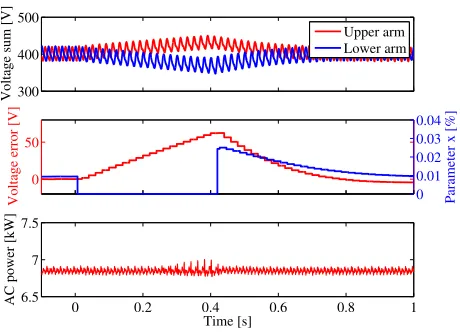
Figs. 15, 16 and 18 are captured for the nominal controller gains (Table III) and a pulse occurring 1.7msafter the phase A grid voltage positive zero crossing. Figure 15 presents the phase A grid voltage and current together with the DC voltage and current (vAs, iA, vDC and iDC in Figure 1)
before and after activation of the pulsed load. Figure 16 presents the grid power and the DC power under steady-state conditions with the pulsed DC load, measured with the HPI. The AC power shows little variation in the presence of the pulsed load while the DC power has a significant droop at the pulse instant. The AC power fluctuation is about 1.65%. The steady-state waveforms obtained correspond to xA,B,C
values of 0.0098, 0.0007 and -0.0156. The peak values of the corresponding 50Hz components in the circulating currents are 0.39A, 0.07A and 0.42A.
A i As DC DC
[image:7.612.58.293.300.372.2]No load Full pulsed load
Fig. 15.Experimental converter waveforms captured by the oscillo-scope: Phase A current, phase A voltage, DC current and DC voltage.
A second set of experimental results is presented in order to validate the dependence of the steady-state values of the balancing controller on the design of the circulating current controller and to confirm the design of the balancing controller and its dynamic performance as discussed in Section V.
6.8 6.9 7
AC power [kW]
0 0.05 0.1 0.15 0.2
5 6 7 8
DC power [kW]
Time [s]
Fig. 16. Experimental converter AC and DC side power captured using the HPI, under steady-state operation with pulsed load.
0 0.2 0.4
Circulating current 50Hz amplitude [A]
−0.6 −0.4 −0.2 0
Circulating current 50Hz ph. shift [rad]
nominal 5*kcirc_i kcirc_i/5 1.8*kcirc_p kcirc_p/2 −0.02
0 0.02
Parameter x
phase A phase B phase C
Fig. 17.The phase A, B and C circulating current 50Hzcomponent
amplitudes and phase shift (computed for the phase A) andx
[image:7.612.327.554.349.491.2] [image:7.612.316.553.550.694.2]300 400 500
Voltage sum [V]
Upper arm Lower arm
0 50
Voltage error [V] 0
0.01 0.02 0.03 0.04
Parameter x [%]
0 0.2 0.4 0.6 0.8 1 6.5
7 7.5
AC power [kW]
[image:8.612.59.289.56.222.2]Time [s]
Fig. 18. Experimental validation of Phase A arm balancing control dynamics (HPI waveforms): sum of the cell capacitor voltages in the upper and lower arm (top plot), difference between the sum of the
upper and lower arm cell capacitor voltages averaged at 20ms and
xparameter (middle plots) and AC power fluctuation (bottom plot).
A. Effect of circulating current control parameters
The circulating current controller gains are varied within the controller stability region, to obtain the dependence of the steady state xA,B,C values and the circulating current 50 Hz
component as presented in Figure 17. The values obtained show trends that are similar to those predicted analytically and found by simulation in Figure 12, having the highest circulating current amplitude for the highest phase shift angle and the highest-parameterxvalues for the highest bandwidth of the circulating current controller.
B. Arm balancing controller dynamics
To complete the validation of the proposed arm balanc-ing controller design, a further experimental test has been performed yielding the results given in the HPI acquisition shown in Figure 18 where the MMC operates under pulsed DC load with nominal control gains from Table III and the arm balancing control is temporarily disabled. The purpose of the test is twofold: first, by disabling the balancing controller the rapid deviation of the upper and lower arm voltages from their nominal value can be appreciated, highlighting the need for balancing to avoid overmodulation; second, once the balancing controller is re-enabled, its transient response can be evaluated and compared with the design target. In Figure 18, the arm balancing is disabled from t = 0 s to t = 0.4 s and then enabled. The convergence of the voltage error, after re-enabling the arm balancing controller, is in agreement with the expected bandwidth of7.3[rad/s]given in Table III, since the fall time of the error can be estimated as tf ≈0.39 s.
VIII. CONCLUSION
This paper presents a new arm balancing method suitable for the operation of an MMC grid-interface for the klystron modulators used in the Compact Liner Collider (CLIC). The modulators represent a pulsed DC load for the converter, with a pulse repetition frequency of 50Hz. The correspondence
between pulse repetition frequency and AC grid frequency necessitates the use of arm balancing controllers in the MMC that have to be incorporated into a suitable control algorithm. A decoupled AC and DC side control has been adapted for the specific conditions and requirements of the application, while the modulation strategy is augmented in order to cope with the imbalances caused by the pulsed load. By employing the presented strategy, low AC power fluctuation can be achieved under pulsed DC load conditions.
The proposed control algorithm is effective and achieves its objectives with very low control complexity, since there is no need for generating and tracking sinusoidal circulating current references. The proposed method has been discussed in detail, including the modelling and design of the balancing controller. Moreover, the effects of the circulating current control design on the steady state operation of the balancing control have been discussed.
The proposed strategy has been initially validated in simu-lation for the full ratings of the CLIC application, achieving capacitor voltage balancing and AC power fluctuation below 0.3%. A 7kW small scale prototype has been developed to experimentally prove the effectiveness of the proposed approach. Experimentally, the measured AC power fluctuation is still below 2%despite the reduced number of voltage levels available in the experimental converter. The dynamic response observed in the experimental converter is in agreement with the theoretical expectation, confirming the analysis and proce-dures used in the design.
REFERENCES
[1] D. Aguglia, C. Martins, M. Bastos, D. Nisbet, D. Siemaszko, E. Sklavounou, and P. Viarouge,Klystron modulator technology challenges for the compact linear collider (clic), in Proc. of IEEEPulsed Power Conference (PPC), Chicago, USA, pp. 1413-1421, 2011.
[2] M. Jankovic, A. Watson, J. Clare, P. Wheeler and D. Aguglia, Grid interface challenges and candidate solutions for the Compact Linear Collider’s (CLIC) klystron modulators, in Proc. of IEEEPulsed Power Conference (PPC), San Francisco, USA, CD-ROM paper, 2013. [3] M. Jankovic, A. Watson, J. Clare, P. Wheeler, and D. Aguglia, Grid
Interface Design for the Compact Linear Collider (CLIC), in Proc. of
Power Electronics and Applications (EPE), Geneva, Switzerland, CD-ROM paper, 2015.
[4] A. Lesnicar, and R. Marquardt,An innovative modular multilevel con-verter topology suitable for a wide power range, inPower Tech Confer-ence Proceedings, Bologna, Italy, CD-ROM paper, 2003.
[5] S. Norrga, L. Angquist, K. Ilves, L. Harnefors, and H.-P. Nee,Decoupled steady-state model of the modular multilevel converter with half-bridge cells, in 6th IET International Conference on Power Electronics, Ma-chines and Drives (PEMD 2012), Glasgow, UK, CD-ROM paper, 2012. [6] M. Zygmanowski, B. Grzesik, and R. Nalepa,Capacitance and induc-tance selection of the modular multilevel converter, in Proc. ofPower Electronics and Applications (EPE), Lille, France, CD-ROM paper, 2013. [7] F. C. Magallanes, D. Aguglia, P. Viarouge, C. de Almeida Martins, and J. Cros, Design of a Solid-State Fast Voltage Compensator for klystron modulators requiring constant AC power consumption, in Proc. ofInternational Power Modulator High Voltage Conference - IPMHVC 2014, Santa Fe, USA, CD-ROM paper, 2014.
[8] M. Hagiwara and H. Akagi, Control and Experiment of Pulsewidth-Modulated Modular Multilevel Converters, in IEEE Trans. on Power Electronics, vol. 24, pp. 1737-1746, 2009.
[10] M. Jankovic, A. Costabeber, A. Watson and J. Clare, Arm Balancing Control and Experimental Validation of a Grid Connected MMC with Pulsed DC Load, in IEEE Trans. onIndustrial Electronics, vol. PP, Issue: 99, 2017.
[11] A. Lachichi and L. Harnefors,Comparative analysis of control strategies for Modular Multilevel Converters, in IEEE9th International Conference on Power Electronics and Drive Systems (PEDS 2011), Singapore, Singapore, pp. 538-542, 2011.
[12] M. Hagiwara, R. Maeda, and H. Akagi, Control and Analysis of the Modular Multilevel Cascade Converter Based on Double-Star Chopper-Cells (MMCC-DSCC), in IEEE Trans. onPower Electronics, vol. 26, pp. 1649-1658, 2011.
[13] A. Hassanpoor, L. Angquist, S. Norrga, K. Ilves, and H. P. Nee,
Tolerance Band Modulation Methods for Modular Multilevel Converters, in IEEETransactions on Power Electronics, vol. 30, pp. 311-326, 2015. [14] M. A. Perez, R. Lizana, and J. Rodrguez, Decoupled current control of modular multilevel converter for HVDC applications, inIEEE Inter-national Symposium on Industrial Electronics (ISIE 2012), Hangzhou, China, pp. 1979-1984, 2012.
[15] J. Pou, S. Ceballos, G. Konstantinou, V. G. Agelidis, R. Picas and J. Zaragoza,Circulating Current Injection Methods Based on Instantaneous Information for the Modular Multilevel Converter, in IEEE Trans. on
Industrial Electronics, vol. 62, pp. 777-788, 2014.
[16] S. Fan, K. Zhang, J. Xiong, and Y. Xue,An improved control system for modular multilevel converters with new modulation strategy and voltage balancing control, in IEEE Transactions onPower Electronics, vol. 30, pp. 358371, Jan 2015.
[17] Gene F. Franklin, David J. Powell, and Abbas Emami-Naeini. 2001.
Feedback Control of Dynamic Systems (4th ed.). Prentice Hall PTR, Upper Saddle River, NJ, USA.
[18] M. Jankovic, A. Watson, J. Clare, P. Wheeler and D. Aguglia, Grid interface design for the Compact Linear Collider (CLIC), 2015 17th European Conference on Power Electronics and Applications (EPE’15 ECCE-Europe), Geneva, 2015, pp. 1-10.
[19] A. Beddard, M. Barnes, and R. Preece,Comparison of Detailed Mod-eling Techniques for MMC Employed on VSC-HVDC Schemes, in IEEE Transactions onPower Delivery, vol. 30, pp. 579-589, April 2015. [20] M. Rejas, L. Mathe, P. D. Burlacu, H. Pereira, A. Sangwongwanich, M.
Bongiorno and R. Teodorescu,Performance comparison of phase shifted PWM and sorting method for modular multilevel converters, in Proc. ofPower Electronics and Applications (EPE’15 ECCE-Europe), Geneva, Switzerland, CD-ROM paper, 2015.
[21] M. A. Perez, S. Bernet, J. Rodriguez, S. Kouro and R. Lizana,Circuit Topologies, Modeling, Control Schemes, and Applications of Modular Multilevel Converters, in IEEE Trans. onPower Electronics, vol. 30, pp. 4-17, 2015.
[22] J. Pou, S. Ceballos, G. Konstantinou, G. J. Capella and V. G. Agelidis,
Control strategy to balance operation of parallel connected legs of modular multilevel converters, in Proc. of International Symposium on
Industrial Electronics - ISIE 2013, Taipei, Taiwan, CD-ROM paper, 2013.
Marija Jankovic(S’10-M’17) was born in Valjevo, Serbia in 1988. She received the B.Sc. and M.Sc. in electrical engineering and computer science at the University of Belgrade, Serbia in 2010 and 2011, respectively; and the Ph.D. degree in electrical and electronic engineering at the University of Notting-ham, UK in 2017.
From 2016 she has been working as a Research Fellow with the Power Electronics, Machines and Control Group, at the University of Nottingham. Her research interests include high power multilevel topologies, converter modelling and control.
Alessandro Costabeber (S’09-M’13) received the Degree with honours in Electronic Engineering from the University of Padova, Italy, in 2008 and the Ph.D. in Information Engineering from the same university in 2012, on energy efficient architectures and control for future residential microgrids.
In 2014 he joined the PEMC group at the University of Nottingham, UK as Lecturer in Power Electronics. His current research interests include modular multilevel converters for HVDC, high power density converters, control and stability analysis of AC and DC microgrids.
Dr. Costabeber received the IEEE Joseph John Suozzi INTELEC Fellowship Award in Power Electronics in 2011.
Alan Watson (S’03-M’08) received his MEng (Hons) degree in Electronic Engineering from the University of Nottingham in 2004 before pursuing a PhD in Power Electronics, also at Nottingham.
In 2008, he became a Research Fellow in the Power Electronics Machines and Control Group, working on the UNIFLEX project (http://www.eee.nott.ac.uk/uniflex/). Since 2008, he has worked on several projects in the area of high power electronics including high power resonant converters, high voltage power supplies, and multilevel converters for grid connected applications such as HVDC and FACTS. In 2012 he was promoted to Senior Research Fellow before becoming a Lecturer in High Power Electronics in 2013. His research interests include the development and control of advanced high power conversion topologies for industrial applications, future energy networks, and VSC-HVDC.
Jon C. Clare (M’90-SM’04) was born in Bristol, U.K., in 1957. He received the B.Sc. and Ph.D. degrees in electrical engineering from the University of Bristol, Bristol.
From 1984 to 1990, he was a Research Assistant and Lecturer with the University of Bristol, where he was involved in teaching and research on power electronic systems. Since 1990, he has been with the Power Electronics, Machines and Control Group, University of Nottingham, Nottingham, U.K., where he is currently a Professor of power electronics. His research interests include power-electronic converters and modulation strategies, variable-speed-drive systems, and electromagnetic compatibility.