NOVEL SOLID-STATE MILLIMETRE-WAVE SOURCES
Malcolm R. Robertson
A Thesis Submitted for the Degree of PhD
at the
University of St Andrews
1993
Full metadata for this item is available in
St Andrews Research Repository
at:
http://research-repository.st-andrews.ac.uk/
Please use this identifier to cite or link to this item:
http://hdl.handle.net/10023/15038
A thesis presented by
Malcolm R. Robertson, BSc.
to the
University of St. Andrews
in application for the degree of
Doctor of Philosophy
July 1992
All rights reserved
INFORMATION TO ALL USERS
The quality of this reproduction is dependent upon the quality of the copy submitted.
In the unlikely event that the author did not send a com plete manuscript and there are missing pages, these will be noted. Also, if material had to be removed,
a note will indicate the deletion.
uest
ProQuest 10166561
Published by ProQuest LLO (2017). Copyright of the Dissertation is held by the Author.
All rights reserved.
This work is protected against unauthorized copying under Title 17, United States C ode Microform Edition © ProQuest LLO.
ProQuest LLO.
789 East Eisenhower Parkway P.Q. Box 1346
I hereby certify that this thesis has been composed by myself, that it is a record of my own work, and that it has not been presented for partial or complete fulfilment of any other higher degree.
This research was carried out in the Department of Physics and Astronomy at the University of St.Andrews under the supervision of Dr J.C.G.Lesurf.
M.R.ROBERTSON JULY 1992
I hereby certify that Malcolm Robert Robertson has fulfilled the conditions of the Resolution and Regulations appropriate to the degree of Doctor of Philosophy.
A Study of some principal solid-state millimetre-wave sources was carried out, using mainly quasi-optical techniques developed at St.Andrews. A review of the theory of operation of Gunn oscillators was undertaken, and a number of wideband tunable Gunn oscillators were buüt, incorporating Gunn diodes from several different manufacturers. Characterisation of their frequency range, power output, bias tuning, and frequency stability were measured. Effects such as bias oscillations and frequency jumps were also noted, and the iterative techniques required to build an oscillator to a
certain specification were presented.
Frequency multipliers are widely used to extend the frequency range of solid-state oscillators, and the techniques used to design frequency multipliers were studied. The use of non-linear capacitors (varactor diodes), and non-linear resistors (varistors and resonant-tunneling diodes) was considered in some detail. An experimental doubler block was designed and built, and doubling using both varactors and varistors was measured and evaluated.
A number of resonant-tunneling double-barrier diodes, or quantum-well devices, was made available through collaboration with Nottingham University. The tunneling process in these devices is inherently fast, making these devices suitable for high-frequency operation as detectors, oscillators, multipliers and mixers. The theory of operation of double-barrier diodes was studied, and methods of evaluating their maximum oscillation frequency were compared. Several different devices were mounted in a whisker-contacted waveguide circuit, and oscillations at W-band were measured. A whisker-contacted multiplier block was designed and buüt, and zero-bias tripling to 254GHz was observed. Resonant-tunneling diodes were also shown to be capable of acting as self-oscillating mixers at W-band. Effects such as injection locking and chaotic oscillations were measured.
Page
1. Millimetre Wave Applications
1.1. Introduction 1
1.2. Some Principal Millimetre Wave Applications 1
1.2.1. Radar 1
1.22. Remote Sensing 2
1.2.3. Communications 2
1.2.4. Plasma Diagnostics 3
7.2.5. Materials Measurement 4
1.2.6. Radio Astronomy 4
1.3. Sources of Radiation 4
1.3.1. Far Infra-Red Lasers 5
1.3.2. Vacuum Tube Devices 5 1.3.3. Solid-State Devices 6
Chapter 1 References 8
2. Gunn Oscillators
2.1. The Gunn Diode 11
2.1.1. The Gunn Effect 11
2.1.2. Modes of operation 13
2.1.3. Cathode Structures 13
2.1.4. Harmonic Operation 15
2.1.5. Device Design and Thermal Considerations 15
2.2. Gunn Oscillators 17
2.2.1. Impedance Matching 17
2.2.2. Oscillator Circuits 19
Chapter 2 References 23
3. Gunn Diode Characterisation
3.1. The Oscillator Block 24
3.1.1. General Description 24
3.1.2. The Choke Structure 25
3.2. Measurement of GEC Prototype Gunn Diodes 27
3.2.1. Device Description 27
3.2.5. Bias Oscillations 3.2.6. Bias Tuning
3.3. Measurement of Thomson and Varian Gunn Diodes
3.3.1. Wide-BandInP High-power Oscillator 3.3.2. Narrow-BandInP High-Power Oscillator
3.3.3. Narrow-Band High-Power High-Frequency Oscillator
Chapter 3 References
37 38 42 42 44 45 47
4. Theory of Quantum Well Devices
4.1. Low Dimensional Structures
4.2. Vertical Transport - Electron Tunneling 4.3. The Double Barrier Diode
4.4. Negative Resistance
4.5. Tlie mechanism of tunneling, and theoretical frequency limits 4.6. Novel Tunneling Structures
Chapter 4 References
48 49 51 54 55 69 72
5. Frequency Multiplication
5.1. Introduction 5.2. The Varactor Diode
5.3. General Multiplier Equations 5.4. Varactor Figures of Merit 5.5. Circuit Design
5.6 Multiplication in Non-Linear Resistances 5.7. Quantum-Well Multipliers
Chapter 5 References
75 75 80 81 83 88 89 93
6. Waveguide Frequency Doublers
6.1. Introduction
6.2. Pump Oscillator Design 6.3. Doubler Design
6.4. The Varactor Bias Supply 6.5. Pump Oscillator Characteristics 6.6. Varactor Doubler Measurements 6.7. Varistor Doubler Measurements
7. QW Devices as Detectors
7.1. Introduction 118
7.2. Layer Structure 118
7.3. Asymmetric IV Characteristics 120
7.4. Large Diameter Devices 123
7.5. Smaller Diameter Devices 125
7.6. Sensitivity 130
7.7. Conclusion 130
Chapter 7 References 132
8. QW Oscillators
8.1. Introduction 133
8.2. Device Layer Structure 133
8.3. Diode Circuit 134
8.4. W-band Oscillation 136
8.5. Conclusion 141
Chapter 8 References 143
9. QW Multipliers
9.1. Introduction 144
9.2. Device Layer Structure 144
9.3. Multiplier Circuit Design 147
9.4. Frequency Multiplication 149
9.5. Conclusion 153
Chapter 9 References 154
10.
Self-Oscillating Mixing and Chaotic Oscillations ii
Quantum Well Double Barrier Diodes
10,1. Introduction 155
10.2 Device Layer Structure 155
10.3. Diode Circuit 157
10.4. Test Circuit 158
10.5. Self-Oscillating Mixing 159
10.9. Upper and Sub-Harmonics and Quasi-Chaotic Behaviour 163
10.10. Conclusion 175
Chapter 10 References 176
11. Chaotic Systems and Noise Sources
11.1. Introduction 177
11.2. Chaotic and Semi-Chaotic Processes 177
11.3. Possible Applications 180
113.1. Radar Applications 181
11.3.2. Communications 181
11.3.3. Noise Sources 181
11.4. Modelling Non-Linear Processes 182
11.5. Gunn Diodes as Noise Sources 183
11.6. Double-Barrier Diodes as Noise Sources 185
11.7. Conclusion 185
Chapter 11 References 186
BWO Backward Wave Oscillator
CW Continuous Wave
DBD Double Barrier Diode
DFTS Dispersive Fourier Transform Spectroscopy
EGA Electron Cyclotron Absorption
ECE Electron Cyclotron Emission
ECRH Electron Cyclotron Resonance Heating
EEL Free Electron Laser
FIR Far Infra Red
FM Frequency Modulation
FWHM FuU Width Half Maximum
IF Intermediate Frequency
IHS Integral Heat Sink
IMPATT Impact Avalanche Transit Time
JCMT James Clerk Maxwell Telescope
LDS Low Dimensional Structure
MBE Molecular Beam Epitaxy
MOCVD Metal-Organic Chemical Vapour Deposition
MPI Martin-Puplett Interferometer
NDC Negative Differential Conductance
NDR Negative Differential Resistance
NPL National Physical Laboratory
PSD Phase Sensitive Detection
QW Quantum Well
Qwrrr
Quantum Well Injection Transit TimeRF Radio Frequency
SIS Semiconductor-Insulator-Semiconductor
lED Tranferred Electron Device
VSWR Voltage Standing Wave Ratio
7.7. Introduction.
The millimetre and submillimetre wave parts of the electromagnetic spectrum lie between the microwave region and the far infra-red. MÜHmetre waves cover the range from 30GHz to 300GHz while submillimetre waves extend upwards to frequencies approaching ITHz. In some respects the millimetre wave region is a transitional one where techniques are borrowed both from microwave technology - for example, the use of waveguide structures - and from optics, which has contributed to areas such as quasi-optics and resonator design. Yet millimetre wave techniques are not totally similar to either the microwave or the FIR regions; they have their own unique characteristics. The full exploitation of the millimetre and submillimetre band has lagged behind neighbouring frequency bands mainly because of a lack of sources. The purpose of this introductory section is to outline major areas of interest within this frequency band, and to describe briefly the type, frequency coverage and relative merits of millimetre and submillimetre wave sources.
7.2. Some Principal Millimetre Wave Applications.
1.2.1. Radar.
Millimetre wave radar has its origins in the microwave radars developed during World War II which operated up to X-band (lOGHz). The trend towards ever higher operating frequencies was stimulated largely by the military who recognised the particular advantages which millimetre wave radar can offer; namely small size, high bandwidth, low beamwidth, better resolution, increased immunity from interference or interception, and penetration of adverse atmospheric conditions, especially smoke and dust. The choice of radar operating frequency is influenced by the atmospheric attenuation characteristics in the millimetre wave region. Absorption by atmospheric gases such as water (H2O), carbon dioxide (CO2), oxygen (O2) and ozone (O3)
220GHz, and most research and development effort has been concentrated at these frequencies as a result [1,2].
While military applications for millimetre wave radar technology such as missile guidance systems continue to expand, there are also some important applications in the civilian sector. One specific area which could attract much commercial interest is that of anti-collision radar for automobiles which has already been demonstrated at 50-60GHZ in Japan [3].
1.2.2. Remote Sensing.
Examples of remote sensing in the millimetre wave region include measurements of the propagation characteristics of the atmosphere in the presence of water vapour at 96GHz [4] and at frequencies up to 246GHz [5]. Measurements have also been carried out to determine the backscatter characteristics of snow surfaces at 215GHz [6] and to measure raindrop sizes [7]. Other forms of environmental monitoring in the millimetre and submillimetre wave regions include sea surface temperature distributions, land surface temperature, crop and soil distribution, measurement of the ozone distribution in the atmosphere, and of the 'greenhouse gases' responsible for the deterioration of the ozone layer [8].
1.2.3. Communications.
The very large bandwidths offered by moving to higher carrier frequencies makes the use of millimetre waves for communications an attractive prospect, bearing in mind the limitations imposed by atmospheric attenuation [9]. Long distance communication links at millimetre wave frequencies perform better in the upper atmosphere where the effects of attenuation are less, which together with the small component size makes such a hnk between two satellites feasible.
The absorption bands, where attenuation is very high, may also be exploited to provide secure short range communications. The strong O2 resonance at 60GHz is a
aircraft-to-aircraft communications, artillery battery communications and local area information distribution [10].
Civilian applications of millimetre wave communication systems have been examined in the context of local area television distribution. British Telecom has investigated both street-level distribution and small town community coverage at frequencies of 30 and 60GHz [11].
1.2.4. Plasma Diagnostics.
For typical tokamak plasmas the electron cyclotron frequency and its harmonics lie in the millimetre and submillimetre region. Measurement of the electron cyclotron emission (ECE) is a valuable diagnostic technique which yields the electron temperature from the intensity of the detected radiation, and the magnetic field strength from the frequency of the radiation [12]. Given a knowledge of the topology of the plasma, it is possible to determine the electron temperature and pressure as a function of position in the plasma.
Another important measurement commonly made is of the electron density in the plasma. High density plasmas are transparent if the plasma frequency cOp is less than the frequency CO of the probing wave [13]. The plasma frequency is proportional to the square root of the plasma density; hence the probing radiation will propagate through areas of low density and will reflect off areas of high density [14]. Using interferometric techniques to determine the time of flight of the incident radiation enables a density 'map' of the plasma to be built up. Alternatively, the same technique may be used to observe density fluctuations at a particular point.
The optical constants of materials at millimetre and submillimetre wavelengths may be measured accurately in a number of different ways, the most important of which is Dispersive Fourier Transform Spectrometry [16,17]. This technique, in which the sample is placed in one arm of a two-beam interferometer, yields both phase and amplitude information, and is applicable to gases, liquids and solids. The sample may be measured either in transmission or reflection. Quantities measured by DFTS include the refractive indices of gases and liquids and the complex permittivities of solids.
1.2.6. Radio Astronomy.
Typically, astronomical observations in the millimetre and submillimetre wavelength region are of gas and dust clouds, and the rotational spectra of molecules therein. Telescopes operating in this region, such as the James Clerk Maxwell Telescope (JCMT) on Mauna Kea, normally have a range of receivers to cover the frequency bands of interest. Between September 1990 and February 1991, for example, the JCMT had receivers available to cover the 220-280GHz, 320-370GHz and 460-490GHz bands; the 690GHz and 800GHz windows; and a bolometer system for continuum observations over a range of wavelengths from 2mm to 0.35mm [18]. Heterodyne receiver systems require a stable, low-noise local oscillator source at the frequency of interest, and extremely sensitive mixers/detectors such as Schottky-barrier or SIS devices operating at liquid helium temperatures [eg. 19,20].
1,3. Sources of Radiation.
Lasers operating in the far infra-red tend to fall into two main categories: optically pumped molecular lasers, and free electron lasers. Optically pumped molecular lasers use a pump source such as a CO2 laser to achieve inversion to the excited level. The
laser lines themselves correspond to a changes between rotational states of the molecules in the lasing medium which can result, in some cases, in the production of many discrete spectral lines. Optically pumped FIR lasers range in frequency from about 4,5THz (D2O) to 250GHz (C^^HjF), (although they are normally in use above
about 600GHz) and can produce very high powers, especially in pulsed operation where power output can be IMW or more [21]. In CW operation, the output powers are considerably less.
Free electron lasers are lasers in which the active medium is a stream of electrons. Radiation is produced from the stimulated backscattering of a low frequency pump (eg. a spatially periodic magnetic field, or a propagating electromagnetic field) from a relativistic electron beam [22]. The output frequency can be tuned by varying either the energy of the electron beam or the frequency of the pump. Power output from free electron lasers can be in the region of megawatts - for example, Columbia University achieved 8MW peak power at 200GHz. FEL's are normally operated at much higher frequencies however, and it is theoretically possible to construct a visible light free electron laser.
1.3.2. Vacuum Tube Devices.
Vacuum tube microwave and millimetre wave devices vary widely in frequency and power output. Klystrons are available up to about 200GHz at tens or hundreds of milliwatts of power, and magnetrons operate at lower frequencies up to about lOOGHz at powers up to IkW. Gyrotrons operate throughout the millimetre wave region at very high peak powers around a megawatt, and are used in high power applications such as plasma heating [23].
electromagnetic energy [24], The BWO is tuned in frequency by varying the beam voltage. Very large tuning ranges are common for BWO’s, sometimes as much as a whole waveguide band. In addition, BWO's operate over the whole of the millimetre and submillimetre band at power levels of a few milliwatts to a few hundred milliwatts. However, BWO's require power supplies of a few kV, tend to have large amounts of FM noise, and have a hmited lifetime.
1.3.3. Solid State Devices.
The two principal types of solid state device used as millimetre wave sources are IMPATT diodes and Gunn diodes. IMPATT is an acronym which stands for IMPact Avalanche Transit Time. IMPATT devices act as oscillators and amplifiers because of a frequency dependent negative resistance arising from the phase delay between the current and voltage waveforms, due to the avalanche breakdown and transit time effect [25]. IMPATT's can operate up to about 200GHz at powers of a few milliwatts. At lower frequencies, their power output can be much higher, especially when operated in pulsed mode.
Gunn diodes take their name from J.B.Gunn, who first reported current oscillations in a slice of GaAs in 1963 [26]. A more descriptive but less common name is the Transferred Electron Device or TED. Its operation depends on the transfer of conduction band electrons from a low-energy, high-mobility state to a high-energy, low-mobüity state, resulting in a bulk negative resistance and the conversion of DC to RF energy. Gunn oscillators are available up to about 150GHz at power levels of a few milliwatts. A typical 94GHz diode will give a few tens of milliwatts of power, and can have very low FM noise [27].
Solid state devices offer certain advantages over FIR lasers and vacuum tube devices, the most obvious being size, cost, robustness, power consumption and longevity. Their disadvantages are mainly that power levels are generally much lower than those available from tube devices, and as yet the maximum oscillation frequencies are lower, Gunn oscillators have proved themselves to be reliable, low noise, widely tunable devices capable of producing adequate amounts of power for a range of apphcations. Their frequency range is very often extended by a factor of two or three with solid state multipliers based on varactor or varistor diodes. IMPATT diodes are capable of higher power output but are prone to suffer from noise originating from the avalanche process itself, and tend to be unreliable. Quantum well devices are still in their infancy, but the tunneling process has been demonstrated to be very fast, with future applications as high frequency oscillators, detectors, mixers and multipliers.
[1] S.L.Johnston, ed., Millimett'e Wave Radar. Dedham, MA: Artech House, Inc, 1980.
[2] R.W.McMillan, C.W.Trussell,Jr., R.A.Bohlander, J.C.Butterworth, and R.E.Forsythe, "An Experimental 225GHz Pulsed Coherent Radar", IEEE Trans. Microwave Theory Tech., vol. 39, no.3, pp. 555-562, 1991.
[3] S.Kitazume and H.Kondo, "Advances in Millimeter-Wave Subsystems in Japan",
IEEE Trans. Microwave Theory Tech., vol.39, no.5, pp. 775-781, 1991.
[4] T.Manabe, R.O.Debolt, and H.J.Liebe, "Moist-Air Attenuation at 96GHz Over a 21-km Line-of-Sight Path", IEEE Trans. Antenna Propagat., vol. 37, no.2, pp. 262-266, 1989.
[5] H.J.Liebe, T.Manabe, and G.A.Hufford, "Millimeter-Wave Attenuation and Delay rates Due to Fog/Cloud Conditions", IEEE Trans. Antenna Propagat., vol. 37, no. 12, pp. 1617-1623, 1989.
[6] R.M.Narayanan and R.E.McIntosh, "Millimeter-Wave Characteristics of Multilayered Snow Surfaces", IEEE Trans. Antenna Propagat., vol. 38, no. 5, pp. 693-703, 1990.
[7] J.Y.Huang, C.Wang, and Y.P.Wang, "Measurements of Raindrop Sizes and Canting Angles", Int. J. Infrared and Millimeter Waves, vol. 10, no.9, pp.1121-1130, 1989.
[8] N.Keen, "Infrared and Millimeter-Wave Measurements of the Environment: Status and Prospects", Int. J. Infrared and Millimeter Waves, vol. 11, no. 3, pp. 323-353, 1990.
[11] R.G.Blake, "The Use of Millimetre-Waves for Broadband Local Distribution",
I7th European Microwave Conference, Rome, Italy, 1987.
[12] N.C.Luhmann,Jr., "Instrumentation and Techniques for Plasma Diagnostics: An Overview", Infrared and Millimeter Waves, vol.2, K.Button, ed.. New York: Academic Press, 1979.
[13] D.Véron, "Submillimeter Interferometry of High-Density Plasmas", Infi'ared and Millimeter Waves, vol.2, K.Button, ed.. New York: Academic Press, 1979.
[14] A.E.Costley, "Electron Density and Temperature Measurements on Large Tokamaks", 5th National Topical Meeting on High Temperature Plasma Diagnostics, Minsk, 1990.
[15] A.R.Harvey, Private Communication.
[16] J.R.Birch and T.J.Parker, "Dispersive Fourier Transform Spectrometry",
Infrared and Millimeter Waves, vol.2, K.Button, ed.. New York: Academic Press, 1979.
[17] F.I.Shimabukuro, S.Lazar, M.R.Cheminck, and H.B.Dyson, "A Quasi-Optical Method for Measuring the Complex Permittivity of Materials", IEEE Trans. Microwave Theory Tech., vol. MTT-32, no.7, pp.659-665, 1984.
[18] "Protostar", Newsletter of the James Clerk Maxwell Telescope, N o.9,1990.
[19] J.W.Archer, "Multiple mixer, cryogenic receiver for 200-350 GHz", Rev. Sci. Instrum., vol.54, no. 10, pp.1371-1376, 1983.
[21] T.A.DeTemple, "Pulsed Optically Pumped Far Infrared Lasers", Infrared and Millimeter Waves, vol.l, K.Button, ed., New York: Academic Press, 1979.
[22] P.Sprangle, R.A.Smith, and V.L.Granatstein, "Free Electron Lasers and Stimulated Scattering from Relativistic Electron Beams", Infrared and Millimeter Waves, vol.l, K.Button, ed.. New York: Academic Press, 1979.
[23] W.M.Manheimer, "Electron Cyclotron Heating of Tokamaks", Infrared and Millimeter Waves, vol.2, K.Button, ed.. New York: Academic Press, 1979.
[24] G.Kantorowicz and P.Palluel, "Backward Wave Oscillators", Infrared and Millimeter Waves, vol.l, K.Button, ed.. New York: Academic Press, 1979.
[25] H.J.Kuno, "IMPATT Devices for Generation of Millimeter Waves", Infrared and Millimeter Waves, vol.l, K.Button, ed.. New York: Academic Press, 1979.
[26] J.B.Gunn, "Microwave Oscillations of Current in III-V Semiconductors", Solid State Communications, vol.l, no.4, pp.88-91, 1963.
[27] G.M.Smith, "Transferred Electron Oscillators at MM Wave Frequencies And Their Characterisation Using Quasi-Optical Techniques", PhD Thesis, St.Andrews University, 1990.
[28] E.R.Brown, J.R.Sôderstrôm, C.D.Parker, L.J.Mahoney, K.M.Molvar, and T.C.McGill, "Oscillations up to 7 12GHz in InAs/AlSb resonant-tunneling diodes",
2. Gunn Oscillators
2.1. The Gunn diode.
2.1.1. The Gunn Effect.
The Gunn effect relies on the bulk transport properties of a semiconductor. In theory a Gunn diode could be constructed from a uniform length of an appropriate semiconductor between two ohmic contacts, and would show the same properties regardless of the direction of current flow. The name diode, therefore, can be misleading. An alternative name is the Transferred Electron Device, or TED, which more accurately describes the way in which these devices operate.
A number of semiconductors exhibit transferred electron effects, but commercial Gunn diodes are grown from n-type GaAs or InP. The two materials differ in a number of respects [1], but the basic principle of operation remains the same. In both materials there is a transfer of conduction band electrons from the central T valley which is a high mobility, low energy state, into the satellite L valley, a low mobility, high energy state. The current density J arising from an applied field E can be expressed as a sum of the contributions from the two conduction bands
J = oE = (n^ep.^ + n^ep^)E (2.1)
where n^ and |ij are the electron density and mobility of the lower valley, and n^ and |Xj^ are the electron density and mobility of the upper valley. At low applied fields, most of the electrons are in the lower valley, and n^» n,^. As the applied field reaches a certain critical value known as the threshold field, the electrons gain sufficient energy to scatter into the upper valley in which their mobility is lower (and their effective mass is greater), and their drift velocity is lower. Thus the current density will tend to fall
0.53eV
GaAs
0.35eV
Figure 2.1. Schematic of band structure in GaAs and InP.
E
u
L.
3
InP
2
GaAs
0 10 20 30 40
E(kV /cm )
Figure 2.2. Electron drift velocity versus electric field.
2.1.2. Modes of Operation.
As the electric field is increased beyond threshold, accumulations of charge tend to form within the active layer of the Gunn diode. The dynamics of these space charge regions are governed by two principal modes of operation: the classical domain mode, and the accumulation mode [2],
The classical domain mode is normally associated with low frequency Gunn diodes with long active layer lengths. Under a sufficiently high applied field (i.e. above threshold) electrons wdl leave the cathode and accelerate in the direction of the anode. These electrons will start to slow down as they are increasingly scattered into the low mobility satellite valley, and electrons arriving from behind catch up with the slower electrons, creating an accumulation zone. Electrons in front of the accumulation zone tend to move away towards the anode, creating a depletion region. In this way a high field dipole domain forms, which lowers the field below threshold in the rest of the sample thus preventing further domains from forming. The domain travels towards the anode at roughly the saturated satellite drift velocity (about lO^cms"^) until the domain runs into the anode, giving a pulse of current. The fields now are no longer high enough for the domain to exist, the domain disappears, the field rises once more toward threshold, and the process repeats.
Most Gunn diodes working at high frequencies (>20GHz) are believed to operate in some form of accumulation mode. The active layer length of these diodes is small, only a few microns or so long. The accumulation layer is formed at the cathode as before, but, mainly as a consequence of the short length of the device, the high field
now persists as far as the anode - there is no depletion region. Thus a much greater | proportion of electrons in the sample are in the satellite valley, resulting in greater j efficiency compared with the domain mode. In addition, the effective transit velocity rj of small accumulation instabilities have been found to be up to three times greater than f domain velocities [3].
2.1.3. Cathode Structures.
has an ohmic cathode, electrons are injected into the active layer with low energy and high mobility, and have to gain energy before being scattered into the satellite valley. This process takes both space and time, and has an adverse effect on the device efficiency since not aU the active layer exhibits negative resistance, just the latter part nearest the anode. The rest of the active layer thus acts as a series positive resistance (Figure 2.3).
End of cycle
S ta rt of cycle
^
0.8Active Layer
E threshold
y 0.4
0.5 1.
Distance iim (a)
Active Layer
00
1
o> ■§ OIn order to reduce the dead space region and maximise the proportion of the active layer available for rf generation, alternative cathode structures are required. The principal aim is to inject hot electrons directly into the active layer with an energy close to the satellite valley energy, and this is usually achieved by creating a high field current-limiting cathode. This may be realised in a number of ways, for example using a metal contact (similar to a Schottky barrier), a highly-doped spike of varying geometries, graded active layer doping, or a combination of these techniques.
2.1.4. Harmonic Operation.
While the use of current-limiting cathodes leads to improvements in power, efficiency and operating frequency, it is generally accepted that GaAs diodes have an upper fundamental frequency limit of around 75GHz, and InP diodes have a limit of about 140GHz. This frequency limit is determined largely by the rate at which electrons gain or lose energy in the central T valley, as opposed to the inter-valley scattering rate which is much faster. GaAs diodes oscillating at frequencies above 75GHz, therefore, are usually operating in a second harmonic mode, with the diode’s non-linear effects responsible for harmonic generation.
2.1.5. Device Design and Thermal Considerations.
Since the dc-rf conversion efficiency of Gunn diodes is low - about 2% for InP, less than 1% for GaAs - most of the device input power has to be removed as waste heat. Keeping the device length short reduces problems of heat sinking, since long devices must remove heat by thermal conduction through the length of the device. By constructing the device as an integral heat sink (IHS) structure, the active layer may be placed only a few microns from the heat sink (Figure 2.4).
Sputtered Gold
NiGeAu n+3Ubatr»te
n**"buffer— k xT’g^vvvvvvvvvv.vvgg^ n active
ni^confect'—s^inm111nnm11ml -NiGeAu contect
Plated Gold Heatsink
Package Stud
Figure 2.4, Schematic diagram of integral heat sink structure.
Gold lid"
Contact tapes
Annul us
Device structure
Package stud
Screw thread
Figure 2,5. Commercial Gunn diode package.
The diode package must in turn be properly heat sunk to ensure that the active layer temperature does not exceed the maximum rating. Varian, for example, quote active layer temperatures of 260*'C for GaAs diodes and 175“C for InP, If the diode is allowed to operate at temperatures in excess of the maximum ratings, then degradation will occur and the diode will almost certainly fail.
dissipation density because the shunt capacitance of the device will become significant, especially when the active length is short. Parasitic losses such as contact resistance, resistive losses in the semiconductor itself, and skin effect losses all become increasingly significant as the device dimensions become smaller. In general, for a given material (GaAs or InP) the bias voltage and power ouput will fall as the operating frequency rises. This is illustrated in Table 2.1. The values given are for Varian Gunn diodes, both GaAs and InP [4].
InP
Frequencv CGHzl Power fmWl Bias (Max') CV) Current fmAl
35 250-350 12.0 300
56 150-250 10.0 250
94 30-60 7.5-11.0 350
26-40 50-350 7.0 600-1100
58-60 50-100 6.0 1000
92-95 20-35 5.0 800-1000
Table 2.1. Comparison of Electrical Characteristics of Varian Gunn diodes.
The high frequency diodes listed above, i.e. those which oscillate at 94GHz, are operating in the second harmonic mode. Fundamental InP diodes for W-band are also available, both from Varian and other manufacturers. However, 94GHz GaAs diodes are only available as second harmonic devices.
2.2. Gmn Oscillators.
2.2.1. Impedance Matching.
of millimetre wave oscillators the problem to be overcome is one of matching the device to a transmission line whose characteristic impedance differs considerably from the device impedance. Gunn diodes typically have a negative resistance of just a few ohms which needs to be matched to a waveguide which has a characteristic impedance of a few hundred ohms. To achieve this impedance transformation, the diode is embedded in a resonant circuit of some sort. The simplest example of a resonant circuit may be illustrated by the circuit shown in Figure 2.6.
L
R
Figure 2.6. A simple resonant transformer.
From the working of Smith [2], it can be shown that at resonance (i.e. when is real),
- ■
q-'
r*“ (Q +
(2.2)
which indicates the order of Q required to bring about the necessary impedance transformation.
Here, the line will be matched to the load only if X.j.=0. Clearly, this is rarely the case. If a backshort is now placed across the transmission line at a distance 1 behind the load (Figure 2.7) the condition for matching becomes:
Rj. = Zq sm (PL) = (Zq/2) sin (2PL) (2.3)
X
Figure 2.7. Matching of a load to a transmission line with a backshort.
From equation 2.3 we can see that, provided Rj<Zq, the load can be critically
coupled to the transmission line if X j is the appropriate value. In general, it is normally possible to match the reactive part of the impedance across the transmission line with a backshort: however, matching the resistive part can prove to be less straightforward.
2.2.2. Oscillator Circuits.
Device^ Backshort
Figure 2.8. Schematic of inductive post circuit.
The resonant cap circuit is the circuit most commonly found in high frequency Gunn oscillators where the diode and disc form a resonator and impedance transformer. If, in addition, the length of the post above the cap can be altered through the incorporation of a coaxial cavity, the resulting circuit provides the basis for wideband tuneable Gunn oscillators (Figure 2.9).
Resonant
Variable Length Coaxial Cavity
Backshort
Figure 2.9. Schematic of resonant cap circuit with coaxial cavity.
If the waveguide cut-off frequency is arranged to be above the fundamental frequency of the diode, then the fundamental is entirely contained within the coaxial cavity and only harmonics can propagate down the waveguide - usually the second harmonic, although the third harmonic can sometimes be detected. Since the fundamental is fully contained within the cavity, very high Q's (at the fundamental) may be achieved, with the loading principally due to resistive losses in the cavity. The presence of the resonant cap, the dimensions of which have a critical effect on the second harmonic in terms of both power and frequency, will of course mean that the simple coaxial resonance mentioned above is now perturbed by the discontinuity of the cap. The backshort provides a reactive termination for the second harmonic and affects the output frequency to a much lesser extent than in a fundamental oscillator, since the output frequency is determined by the fundamental.
It is important to point out that the second harmonic also operates in a quasi-coaxial mode, so that both the fundamental and the second harmonic are coupled into modes in the coaxial cavity, although the second harmonic is coupled more weakly. Furthermore, since the condition for resonance at the second harmonic is likely to differ from that of the fundamental at a given frequency, with the result that neither of the two modes are truly coaxial. The situation is further complicated by the presence of the cap and its associated capacitance. The impedance transformation at any particular frequency, therefore, is a function of the impedance seen by the quasi-coaxial mode at the second harmonic, as well as a function of the impedance transforming effects of the radial disc [2]. Changing disc parameters such as radius, thickness and height, all affect the impedance transformation in a complex manner. Carlstrom et al [6 ] performed a comprehensive series of measurements in which the
power. Lastly, increasing the thickness of the disc mimics both the effects of increased diameter due to increased fringing capacitance, and of increased height.
Chapter 2 References.
[1] I.G.Eddison, "Indium Phosphide and Gallium Arsenide Transferred-Electron Devices", Infrared and Millimeter Waves, vol. 11, K.Button, ed.. New York: Academic Press 1984.
[2] G.M.Smith, "Transferred Electron Oscillators at MM Wave Frequencies And Their Characterisation Using Quasi-Optical Techniques", PhD Thesis, St.Andrews University, 1990.
[3] D.Jones and H.D.Rees, "Accumulation Transit Mode in Transferred-Electron Oscillators", Electron. Lett, vol.8 , no.23, pp.566-567, 1972.
[4] Varian, Solid State Microwave Division, 3251 Olcott Street, Santa Clara, CA 95054.
[5] W.M.Haydl, "Fundamental and Harmonic Operation of Millimeter-Wave Gunn Diodes", IEEE Trans. Microwave Theory Tech., vol.MTT-31, n o .ll, pp.879-889,
1983.
[6 ] J.E.Carlstrom, R.L.Plambeck, and D.D.Thomton, "A Continuously Tunable
3. Gunn Diode Characterisation
3.1. The Oscillator Block.
3.1.1. General Description.
As mentioned in the previous section, the Gunn oscillator circuits which have been developed at St.Andrews are based on a second harmonic resonant cap design with a variable height coaxial cavity [1-3]. A vertical section through a typical oscillator block is shown schematically in Figure 3.1.
Bias Cormector
PTFE Plug
Micrometer
Glass Bead
Spring
Choke
Coaxial Cavity Output Waveguide
Backshort Gunn Diode
Figure 3.1. Schematic of Gunn Oscillator.
and the next section provides space for the SMA bias connector, over-voltage Zener diode and anti-spike RC network. The centre section contains the coaxial cavity and the output waveguide, and the bottom section houses the diode. A spring-loaded, sliding, contacting backshort is situated behind the diode in the waveguide. The four sections of the block are assembled accurately using precision machined dowels and are held together by stainless steel bolts.
3.1.2. The Choke Structure.
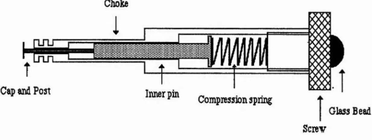
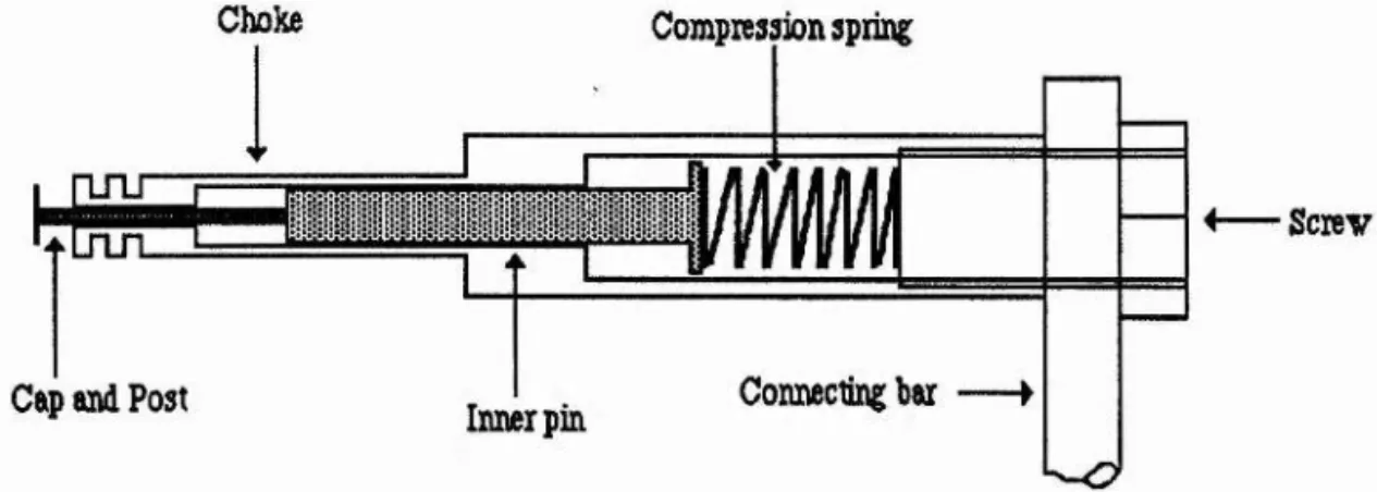
Essentially, the choke structure performs two functions: it slides up and down in the coaxial cavity to tune the frequency of the oscillator, and it carries the bias current to the diode. In order to maintain electrical contact to the diode whatever the position of the choke, the cap and post is spring-loaded as shown in Figure 3.2.
C
hoke
i
i.ECi '(zz
Î
Cep end Post
Inner pin
- fcompression spring
Glass Bead
Screv
Figure 3.2. Detail of spring-loaded cap and post within the choke.
The filter structure at the lower (diode) end of the choke is a low-pass, five section low/high impedance design which has been used successfully by Smith [1]. The cut-off frequency is 15GHz, well below the passband edge. The lengths of the various sections had been calculated both for a maximally flat Butterworth filter and a IdB ripple Chebyshev filter. In practice, it was found that the exact dimensions were not critical, provided that the section lengths were made between ^ / 8 and 3X/8 and
avoided half-wave resonance. Similarly, the difference in radius between the low and high impedance sections should be large so that the reflection coefficient is also large, but should again avoid half-wave resonance. The dimensions of the choke filter are shown in Figure 3.3.
2.93
0.65
1.00 or 0.80
I
I
All dimensions in mm
Figure 3.3. Choke filter dimensions.
The cap and post are machined as a single unit from brass or aluminium. The diameter of the post is either 0 .8mm or 1.0 mm (depending on the particular choke) to
3.2. Measurement of GEC Prototype Gmn Diodes.
3.2.1. Device Description.
This section details the results obtained from measurements perfonned on prototype Gunn diodes supplied by GEC in late 1987. The devices originated from three wafers labelled DB420, DB429 and DB421, all with transit lengths of 1.5|xm. Wafers DB420 and DB429 should be nominally identical since DB429 was a regrowth of DB420. Wafer DB421 has the same injector and transit region as DB420, but the substrate is on the opposite side. This was done as there was a question as to whether the efficiency could be improved by heat sinking the anode. Diodes from DB421 therefore required a negative dc bias supply (Figure 3.4).
Measurements were made on six samples each of DB429 and DB421, and on one sample of DB420. Unfortunately, six of these diodes failed within a few minutes of switch-on - two open-circuit (DB429) and four short-circuit (one DB429, three DB421). This high failure rate was probably due solely to the prototype nature of the diodes.
n+ n+ Transit n+ n+
GaAs Graded Gap Spike n- GaAs Buffer Substrate
DB429 DB420
n+ n+ n+ Transit n*f
Substrate Buffer Graded Gap Spike n- GaAs GaAs DB421
Figure 3.4. Gunn diode layer profile.
3.2.2. Frequencv and Power Measurement.
Two oscillator blocks were used in the characterisation of the diodes. Designated EEV5 and EEV8, the waveguide sizes were WG27 (2.54 x 1.27mm) and WG28 (2.00
cavities. The cap and post dimensions used in all the measurements were a 2.00mm diameter cap, 0 .2 mm thick, on a 0 .8mm post.
Frequencies were measured with a Martin-Puplett polarising interferometer [4] and Golay detector. Power was measured using an Anritsu power meter with a WG27 detector head and WG27/WG28 taper where appropriate. The position of the backshort and the bias voltage were optimised for maximum power at each frequency. In addition, the diodes were raised slightly in the cavity in order to optimise power by improving the impedance matching between the diode and the waveguide. Power-frequency curves are shown in Figures 3.5 to 3.13.
DB420/l/4#linEEV8 3
2
1
0
!
I
Cavity length mm Power mW
70 80 90 100 110 120 130
Frequency GHz
I
I
o
I
I
è
DB429/l/3#2 in EEV8 3
-10
2 -8
1
0
70 80 90 100 110
Frequency GHz
Figure 3.6.
DB429/l/3#4inEEV8 3
- 10
2
1
0
80 90 100 110 120 130 140
Î
I
Î
I
Cavity length mm Power mW
Cavity length mm Power mW
Frequency GHz
I
I
u
DB429/l/3#6inEEV8
3
2
-10
1
0
90 100 110 120
70 80
Frequency GHz
Figure 3.8.
DB421/1/4#! in EHV8 Tuning Down
I
I
!
3
2
1
0
70 80 90 100 110 120 130
I
I
I
I
Cavity length mm Power mW
Cavity length mm Power mW
Frequency (down) GHz
DB421/1/4#1 in EEV8 Tuning Up
I
I
I
I
II
32
0
70 80 90 100 110 120 130
Frequency (up) GHz
Figure 3.10.
DB421/l/4#linEEV5
i
I
3
2 - 10
1
0
70 80 90 100 110 120 130
i
I
Cavity length mm Power mW
Cavity length mm Power mW
Frequency GHz
I
I
uDB421/l/4#3 inEEV5 4
3
-10
2
0
80 110
70 90 100
Ï
I
Frequency GHz
Figure 3.12.
DB421/l/4#5inEEV5 3
2
1
- 2
0
70 80 90 100 110 120
Î
I
Cavity length mm Power mW
Cavity length mm Power mW
Frequency GHz
As a general observation we may say that for a given diode, for example DB421/1/4# 1, we should get most power using the largest possible size of waveguide for the particular frequency of interest. Although it was not possible to measure each diode in both sizes of waveguide, experience has shown that for our particular design of oscillator block, better coupling between the coaxial cavity and the waveguide is achieved with WG27 waveguide rather than WG28, but this will depend to some extent on the individual diode.
3.2.3. Frequencv Jumps and Power Dips.
Most diodes exhibited frequency jumps during tuning, often associated with a significant dip in power. Frequency jumps and dips in power have been reported previously [1-3], a result of the admittance of the diode at the fundamental frequency changing significantly, in particular where the sign of the reactive termination of the second harmonic changes.
In the analysis performed by Smith [1] the resonant condition met when one tunes through a second harmonic resonance is given by
IbJco)I - z ( ^ ) Ib^(2 o))I = B^ = 0 (3.1)
where B^(co) and B^(2(o) are the circuit susceptances at the fundamental and second harmonic frequencies respectively, Vj and V2 are the terminal voltages across
the diode at co and 2 co, and By is the total reactance of the circuit and diode at the
frequency (O,
Normally the second term in Eq.3.1 is small, and the resonant condition will be dominated by the fundamental frequency term. If the second term should become significantly large, either through V2 becoming large (resonance of the second
harmonic in the cavity), or B^(2co) tending towards plus or minus infinity ('anti-resonance'), frequency jumps will occur.
'anti-resonance’ are very small since the second harmonic voltage tends towards zero m this region.
A dip in power in the close vicinity of a frequency jump is to be expected since at a resonance or anti-resonance, the cavity and the waveguide are either significantly over-coupled or under-coupled. However, one should not assume from this that when not in the close vicinity of a frequency jump, the critical coupling condition is satisfied - there is usually a certain amount of under or over-coupling. A peak in the power frequency curve will indicate that critical coupling is either satisfied or very close to being satisfied.
When one compares the experimental results with the curves predicted by theory [1], we see that there is a reasonable amount of agreement, given the inevitable
differences between individual diodes.
Let us now consider the large frequency jump shown by most of the diodes at the high frequency end of the tuning range. Two or three high frequencies (around 120 Ghz, typically) could usually be detected, at very low powers. At this point, the coaxial cavity is extremely short and the diode, the resonant cap and the bottom of the choke are very close to each other - in some cases, the choke may be touching the upper surface of the cap. One may suggest that in this situation some sort of radial mode is set up in place of the normal coaxial mode, causing a frequency jump. In one case, DB429/l/#2 in EEV8 , there was a drop in frequency at the shortest cavity
length. This may either have been due to mechanical stress on the top cap of the diode package, causing slight deformation of the package, or to an increase in the capacitance seen by the diode.
Frequency jumps can also be observed at very long cavity lengths. Diode DB421/1/4#1 in block EEV8 could be made to produce oscillations of 142 GHz at a
frequencies. These are usually obvious, but can sometimes cause modulation of the diode itself.
3.2.4. Current-Voltage Characteristics
I-V curves for four diodes were measured at 94 GHz (Figures 3.14 -3.17). The d.c. resistance of the oscillator block is typically 2 Q, so the actual voltages across the
diode will be slightly less than those shown. The current was read from a 15 V bench supply feeding the diode bias supply, and the quiescent current consumed by the bias supply was subtracted from each current reading. Threshold currents varied between about 700mA and 1000mA, and threshold voltages varied between about 2.5 V and 3.5V. These figures are fairly typical for GaAs devices, although the currents passed by the diodes are a little high, indicating that these diodes are large-area devices with relatively high capacitance.
The sharp upturn of each curve shows where the Zener diode, situated in the top section of the block, starts to conduct.
DB420/l/4#linEEV8 1200
1000
800
t
I
600u 400
200
2 4
0 6 8
Voltage V
<
e
I
DB429/l/3#2inEEV8 1200
1000
800
600
400
200
0
4
Voltage V
Figure 3.15.
DB429/I/3#4inEEV8
Voltage V
1200
1000
800
t
"S 600
u 400
200
2 4 6
0 8
DB429/l/3#6inEEV8 1200
1000
800
e
I
600u 400
200
4
2 6 8
0
Voltage V
Figure 3.17.
3.2.5. Bias Oscillations
Monitoring the bias supply with an oscilloscope showed that every diode suffered from bias oscillations over some part of the negative resistance region. The frequency and amplitude of the bias oscillations varied, but typically were in the region of tens of megahertz, and between 2mV and 20mV peak-to-peak. Usually there were several frequencies present. As the bias voltage was increased to beyond about (±)4.5V, the bias oscillations disappeared.
but due to the current design of our chokes this has not been possible. Attention was therefore focussed on the protection circuit situated in the top section of the oscillator block (Figure 3.18).
+
0
R
Bias Tag
(3 mm.
Diodt
Figure 3.18. Diode protection circuit.
R is typically 22Q and C ranges from 0.1 p.F to O.OljiF. These values were changed over a fairly wide range but had little or no effect. The Zener diode (usually around 6.5V) was removed and then replaced, again with no noticeable effect. Threading several ferrite beads onto the bias tag reduced the amplitude of oscillation for some, but not all, of the diodes.
All diodes operated well once they were biased above a certain level, with no further evidence of bias oscillations. In most applications, therefore, these diodes would not cause any problems. An important exception, however, is bias tuning.
3.2.6. Bias Tuning
Varying a Gunn diode’s bias voltage causes the output frequency to vary as the device capacitance changes. Bias tuning is a widely-used technique in applications such as phase-locking and frequency modulation. It is convenient when measuring the variation of frequency with bias to mix the signal down to a much lower frequency, so that the frequency variations are more easily observed (Figure 3.19).
to produce an intermediate ( IF ) signal of a few hundred megahertz. Both oscillators were set separately to 94 GHz and then connected via two lOdB couplers and an isolator to prevent any modulation of one oscillator by the other. The two signals were mixed by a Flann diode mixer and the d.c. component filtered off to be used as a measure of signal strength. The diode mixer's backshort was adjusted to match impedances, and the IF signal was displayed on a Hewlett-Packard HP8558B spectrum analyzer.
Test Oscillator Feedhorn to interferom eter
J
V ) dc level
Mixer 10db coupler
Reference Oscillator --- ^ IF signal
High Pass Filter
Spectrum Analyser
Figure 3.19. Bias Tuning
The oscillators were switched on and allowed to stabilise thermally. Bias tuning curves were obtained for the three negative top-cap devices (Figures 3.20-3.22). Unfortunately, the presence of bias oscillations made it impossible to tune at voltages below about -4.5V.
Thermally induced frequency shifts were easily seen. Turning one oscillator off to let it cool down and then turning it back on again showed frequency shifts of tens of megahertz as the cavity warmed up. Also noted was the effect the backshort had on frequency, shifting up to 25MHz each way.
DB421/l/4#lin EEV5. Bias Tuning 600
500
400
s
300200
100
8 7 6 -5 4
Bias V
DB421/l/4#3 in EEV5. Bias Tuning
800
800
-400
-200
-8 -7 6 -5 4
BiasV
Figure 3.21.
DB421/l/4#5 in EEV5. Bias Tuning 1000
800
-600
-s
I
400 -200-8 7 6 -5 4
BiasV
Bias tuning is a relatively straightforward way of providing fine control over frequency, but should be treated with caution especially if one is attempting to sweep over a large (more than a few hundred MHz) frequency range. Potential problems include bias oscillations, overheating of the diode leading to premature failure, fluctuations in output power and worsened thermal stability. If fine bias control is required, for example when phase-locking the oscillator, the main requirement is that the bias supply must be stable at the millivolt level, i.e. it must have a very low noise floor.
3.3. Measurement of Thomson and Varian Gunn Diodes.
In the previous section, all of the prototype Gunn diodes were placed in nominally identical circuits in order to compare their performance. However, the more usual procedure when setting up a Gunn oscillator with a particular diode is to employ an iterative process to determine the (critical) cap and post dimensions which give the desired power/frequency characteristics. The graphs provided by Carlstrom et al [2] are a useful guide in the determination of the correct cap dimensions, A summary of their results are set out in Chapter 2.
The majority of the commercially available Gunn diodes used at St.Andrews are bought from Varian [5], with a few acquired from other sources such as Thomson [6 ].
While many of the oscillators built in St. Andrews are for use in our own laboratories, a number have been sold on a commercial basis to Government institutions, research laboratories of large companies, and other Universities. In such cases, the oscillator must be set up to satisfy a certain minimum specification regarding frequency range and the minimum power output over that range. This section details the cap/post dimensions, the type of diode used and other circuit parameters of some of these oscillators. The resulting power/frequency characteristics may be regarded as state of the art.
3.3.1. Wide-Band InP High-Power Oscillator.
harmonie device, and the high-power requirement led to the choice of a Varian 94GHz InP diode, type VSB9122S13. With the diode mounted in a full-height WG27 block with 3mm cavity, the optimum cap diameter was determined to be 2.32mm on a 1.0mm post. As with most oscillators, the diode was raised slightly in the cavity to help optimise the power. The power/frequency characteristics are shown in Figure 3.23.
Kent University Oscillator. 4.0
3.5"
-40
3.0
--20
2.5
-2.0
70 80 90 100
Frequency GHz
I
I
Micrometer mm Power mW Figure 3.23The graph shows that the actual frequency range achieved was about 76GHz to 91 GHz, slightly less than specified. However, the application of the oscillator demanded that useful power at 73.5GHz be available. Consequently, a number of larger diameter caps were manufactured in an attempt to shift the frequency band downwards. This was achieved, but at the expense of the upper end of the frequency band, where 89.5GHz was also a critical frequency. In such cases, the usual course of action is to replace the diode with another nominally identical diode from the same batch. This approach exploits the small differences which always exist between diodes from the same wafer. Using the original 2.32mm diameter cap, the new diode covered a slightly wider frequency range, including 73.5GHz and 89.5GHz, but at the expense of creating a large resonance at around 77GHz and a smaller resonance at around 8 6 GHz (Figure 3.24). Despite these (unavoidable) resonances, the oscillator
i
Recal. Kent University OscUlator
40 5
-30 4
-20
3
2
70 80 90 100
Freq. GHz
Figure 3.24.
3.3.2. Narrow-Band InP High-Power Oscillator.
i
I
Micrometer mm Power mW
I
1
BAe Oscillator
-30
1.2
--20
72 73 74 75 76 77 78
Frequency GHz
Figure 3.25.
Î
I
Micrometer mm Power mW
3.3.3. Narrow-Band High-Power High-Frequencv Oscillator.
Unusually, the Centre National de la Recherche Scientifique in Toulouse did not actually specify the performance they required from this oscillator. Instead, they supplied a 94GHz fundamental InP diode made by Thomson for incorporation into an oscillator. Using an identical circuit to that used for the BAe oscillator yielded the characteristics shown in Figure 3.26. In common with other fundamental oscillators, this oscillator tunes over a rather narrow frequency range (compared with second harmonic devices).
C.N.R.S. Oscillator
5.0 40
4.5 -30
4.0- -20
3.5
86 88 90 92 94 96 98
Frequency GHz
Figure 3.26
Ï
I
Chapter 3 References.
£11 G.M.Smith, "Transferred Electron Oscillators at MM Wave Frequencies And Their Characterisation Using Quasi-Optical Techniques", PhD Thesis, St.Andrews University, 1990.
[2] J.E.Carlstrom, R.L.Plambeck and D.D.Thomton, "A Continuously Tunable 65-115 GHz Gunn Oscillator", IEEE Trans. Microwave Theoiy Tech.., vol. MTT-33, no.7, pp. 610-619, 1985.
[3] W.H.Haydl, "Fundamental and Harmonic Operation of Millimeter-Wave Gunn Diodes", IEEE Trans. Microwave Theory Tech., vol. MTT-31, no.11, pp.879-889, 1983.
[4] D.H.Martin, "Martin-Puplett Interferometric Spectrometers", Infrared and Millimeter Waves, vol.6 , K.Button, ed.. New York: Academic Press 1982.
[5] Varian, Solid State Microwave Division, 3251 Olcott Street, Santa Clara, CA 95054.
[6 ] Thomson-CSF Division Composants Hybrides et Microondes, 29, Avenue