Article
Plasmonic Colour Printing by Light Trapping in
Two-Metal Nanostructures
Keith Wilson, Cristian A. Marocico, Esteban Pedrueza-Villalmanzo, Christopher Smith, Calin Hrelescu and A. Louise Bradley *
School of Physics and CRANN, Trinity College Dublin, Dublin D2, Ireland * Correspondence: [email protected]
Received: 29 May 2019; Accepted: 27 June 2019; Published: 1 July 2019
Abstract: Structural colour generation by nanoscale plasmonic structures is of major interest for non-bleaching colour printing, anti-counterfeit measures and decoration applications. We explore the physics of a two-metal plasmonic nanostructure consisting of metallic nanodiscs separated from a metallic back-reflector by a uniform thin polymer film and investigate the potential for vibrant structural colour in reflection. We demonstrate that light trapping within the nanostructures is the primary mechanism for colour generation. The use of planar back-reflector and polymer layers allows for less complex fabrication requirements and robust structures, but most significantly allows for the easy incorporation of two different metals for the back-reflector and the nanodiscs. The simplicity of the structure is also suitable for scalability. Combinations of gold, silver, aluminium and copper are considered, with wide colour gamuts observed as a function of the polymer layer thickness. The structural colours are also shown to be insensitive to the viewing angle. Structures of copper nanodiscs with an aluminium back-reflector produce the widest colour gamut.
Keywords: plasmonic colour printing; light trapping; two-metal nanostructures
1. Introduction
Unlike traditional color generation methods based on dyes and pigments, the generation of color with nanostructures has become the focus of intense research interest since nanostructures are resistant to photo-bleaching and exhibit superior robustness to chemical, physical and thermal stresses in contrast to dyes and pigments. Moreover, the structural color can be controlled at sub-diffraction-limited dimensions [1], rendering nanostructures as crucial constituents for color generation [2–5] in a broad range of applications, ranging from color printing [1], color filtering [6–9], and anti-counterfeit measures [10] to passive reflective display technologies [11] and imaging sensors [12,13]. Thin film stack structures can generate structural color based on constructive or destructive interference, so that only specific spectral regions of the visible light are reflected back to the observer. Other structures based on very thin layers of highly absorbing materials [14] can absorb certain spectral ranges in the visible generating color based on a subtractive color model. However, for these thin film structures achievable colors palettes are often limited. Noble metal nanostructures exhibiting plasmonic modes, i.e., collective electron oscillations at a dielectric-metal interface which can be resonantly excited with visible, near infrared and infrared light [15–17], can generate all colors across the visible spectrum through the selective scattering and absorption of light [2,5,18]. Plasmonic modes can be localized or can propagate along the dielectric-metal interface [15,16]. The plasmonic modes are strongly dependent on the noble metal selected, the refractive indices of the surrounding media, the dimensions and shape, as well as on arrangement and distribution, of the nanostructures on a substrate [15,19–21]. Structural reflected color generation with structures based on one metallic material has been demonstrated with simple thin film structures [8,14] and periodically nanostructured
Nanomaterials2019,9, 963 2 of 15
metallic films [22,23], with all-metal nanostructures [24,25], with nanohole arrays [26], nanoantenna arrays [1,27–30] or randomly distributed nanoparticles [18,31,32] on top of a back-reflector or on transparent substrates. Plasmonic structural color is attractive for many applications since polarisation dependent [33–36] or independent [23,27] color generation can be achieved depending on the application requirements, such as stereoscopic printing [35]. Likewise viewing angle sensitive or insensitive [31,37] color generation have been demonstrated. Plasmonic printing technology is becoming more attractive commercially as extreme ultraviolet lithographic processes become more widely available, cheaper and scalable [38,39]. Designs compatible with nanoimprint technology can also offer low cost solutions [40]. Plasmonic color generation based on extraordinary optical transmission [6,41,42], Fano-type resonances [43,44], Wood–Rayleigh anomalies or excitation of propagating surface plasmons viagrating coupling is highly depended on the viewing angle as well as on the polarisation of the excitation source, which for some application fields, such as displays, is not desirable. Nanohole and pillar-type nanostructures based on gold, aluminium or silver as sole the plasmonic material have been extensively examined to control generated colors and to extend the achievable color palettes [1,28,35]. Additionally, randomly distributed nanoparticles, exhibiting localised surface plasmon modes, have been demonstrated as strong color filters [31]. However, the random distribution of nanoparticles leads to spectrally broad features in the optical response, and consequently to low color clarity. In contrast, patterned nanostructure arrays can exhibit spectrally narrower features due to the uniform shape and spacing of the nanoparticles in an array configuration. Nanostructures exhibiting spectrally narrow modes are of particular interest in structural color generation. Metal-insulator-metal (MIM) nanoparticle array configurations based on a single plasmonic material have been extensively studied for sensing applications in the IR [45,46] and in the visible spectral range [47–49] as well as for color generation applications [1,27,29,36,43]. However, the achievable color palette with nanostructures using a sole plasmonic material, for both the nanoparticles and as a back-reflector, is often limited. Extension of the achievable color palette is an important consideration to progress plasmonic color generation as an emerging and viable technology for future devices, such as color filters, displays and anti-counterfeit measures. The color palette might be extended with nanostructures comprising two or more plasmonic materials. Surprisingly, to our knowledge, there have been very few studies on plasmonic color generation with nanostructures comprising two different plasmonic materials [32,50–53]. Xiong et al. considered random nanoholes in a Cu film separated from an Al layer [50]. Choi et al. reported on a Au coated anodic aluminium oxide template, producing plasmonic nanopores, on top of an Al film [51], while Stewart et al. recently considered two different plasmonic materials, one used for randomly distributed Ag nanocubes and the other as a Au back-reflector [32].
narrow window (35 nm). Although thinner films can generate red and purple colors, the spectrally narrow feature at around 585 nm for hybrid nanostructures with certain polymer thicknesses is responsible for the green color generation. Green colors can be only achieved for polymer films thicknesses staring from ca. 80 nm onwards, also typical thicknesses for organic optoelectronic devices. Combinations of gold, silver and copper nanodiscs on gold, silver and aluminium back-reflectors are also considered. Structures of copper nanodiscs with an aluminium back-reflector produce the widest color gamut, occupying 66% of the sRGB triangle.
2. Materials and Methods
2.1. Simulations
Simulations were carried out using the commercially available FDTD solver from Lumerical Solutions Inc. (Vancouver, Canada). A broadband plane wave as used for the excitation. The excitation was from the air half-space of the simulation volume, (+z direction in the simulation coordinate system) and p-polarized (parallel to the x-axis). FDTD multi-coefficient fits to experimental data from reference [61] were used for the permittivity of Ag and Si, and to the data from reference [62] for the permittivity of Au. The complex refractive index for the propylene based transparent polymer used in the simulation, was determined by multiple-angle ellipsometry measurements before and after the EBL exposure and chemical lift-offprocess. The spectral dependences ofnandkare shown in Figure S1a,b, respectively, in the Supplementary Materials. With low absorption,k, and a relatively constantnvalue across the visible, it is suitable for thin film interference structures and for maximising the light interaction between the nanodisc array and Ag back-reflector. The boundary conditions in the ±z directions were set to perfect matching layers (PML) optimised for step angles. In the±x and±y
directions the boundary conditions were set to periodic.
2.2. Experimental
Nanomaterials2019,9, 963 4 of 15
thick Au layer was deposited by EB-PVD, at a deposition rate of 0.5 Å/s. Lift-offwas carried out by submersion of the samples for 10 min in Acetone solution heated to approximately 40◦C on a hot plate. This removed the remaining PMMA and unwanted Au from the samples. Before the spectral characterization, the arrays were first examined in reflection with an optical microscope equipped with a 100×objective under bright-field illumination to determine the colour uniformity and eventual surface imperfections. Reflectance spectra were measured using an in-house system. The samples were excited with a xenon lamp under normal incidence using a spot size of approximately 50µm diameter. Multiple angle scan microspot ellipsometry was carried out on an unpatterned area near the arrays to determine the polymer thickness in the fabricated structures, with a lateral spot size diameter of 300µm. The fabricated structures were characterized with a Carl Zeiss Ultra FE-SEM Electron microscope (Carl Zeiss, Oberkochen, Germany). An accelerating voltage of 5 kV was used, at a working distance of 4.9 mm and aperture of 10µm.
3. Results and Discussion
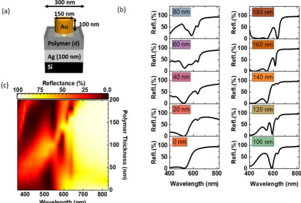
Firstly, a hybrid metallic nanostructure comprising of Au nanodiscs separated by a uniform dielectric layer from a Ag back-reflector is considered. Figure1a shows the schematic of the hybrid structure for color generation. The 100 nm high gold nanodiscs with 150 nm diameter are arranged in square arrays with 300 nm pitch on top of a back-reflector consisting of a polymer thin film and a 100 nm thin silver film on a silicon substrate.
Nanomaterials 2019, 9, x FOR PEER REVIEW 4 of 15
by drying with nitrogen. Subsequently, a 100 nm thick Au layer was deposited by EB-PVD, at a deposition rate of 0.5 Å/s. Lift-off was carried out by submersion of the samples for 10 min in Acetone solution heated to approximately 40 °C on a hot plate. This removed the remaining PMMA and unwanted Au from the samples. Before the spectral characterization, the arrays were first examined in reflection with an optical microscope equipped with a 100 × objective under bright-field illumination to determine the colour uniformity and eventual surface imperfections. Reflectance spectra were measured using an in-house system. The samples were excited with a xenon lamp under normal incidence using a spot size of approximately 50 μm diameter. Multiple angle scan microspot ellipsometry was carried out on an unpatterned area near the arrays to determine the polymer thickness in the fabricated structures, with a lateral spot size diameter of 300 μm. The fabricated structures were characterized with a Carl Zeiss Ultra FE-SEM Electron microscope (Carl Zeiss, Oberkochen, Germany). An accelerating voltage of 5 kV was used, at a working distance of 4.9 mm and aperture of 10 μm
3. Results and Discussion
[image:4.595.142.451.359.567.2]Firstly, a hybrid metallic nanostructure comprising of Au nanodiscs separated by a uniform dielectric layer from a Ag back-reflector is considered. Figure 1a shows the schematic of the hybrid structure for color generation. The 100 nm high gold nanodiscs with 150 nm diameter are arranged in square arrays with 300 nm pitch on top of a back-reflector consisting of a polymer thin film and a 100 nm thin silver film on a silicon substrate.
Figure 1. (a) Schematic of the hybrid nanostructure unit cell: Square arrays (300 nm pitch) of gold
nanodiscs (100 nm high and 150 nm in diameter) on a back-reflector substrate consisting of a polymer thin film on top of a 100 nm thick silver (Ag) layer on silicon. (b) Simulated reflectance spectra of the hybrid structures for increasing polymer spacer thicknesses. The individual generated colours (sRGB) are displayed as insets. (c) Simulated reflectance as function of polymer thickness.
In contrast to pillar-type structures with a small diameter to height ratio, our design is more versatile, easily facilitating the use of different metallic components, and more robust, both during and after fabrication. Moreover, the uniform polymer film protects the back-reflector thin film from degradation. Providing high reflectance, the back-reflector allows for color generation in reflection mode. The dimensions of the gold arrays were chosen according to typical nanofabrication values in order to enable easy fabrication. Besides the easy fabrication aspect, the array period of 300 nm offers two more benefits for color generation. Firstly, since there is a sufficient separation between the nanodiscs, the near field coupling between adjacent nanodiscs is minimal. Secondly, the period is just smaller than the diffraction limit, so our nanostructure does not exhibit diffractive modes and no
Figure 1. (a) Schematic of the hybrid nanostructure unit cell: Square arrays (300 nm pitch) of gold nanodiscs (100 nm high and 150 nm in diameter) on a back-reflector substrate consisting of a polymer thin film on top of a 100 nm thick silver (Ag) layer on silicon. (b) Simulated reflectance spectra of the hybrid structures for increasing polymer spacer thicknesses. The individual generated colours (sRGB) are displayed as insets. (c) Simulated reflectance as function of polymer thickness.
no mode hybridisation [63] is observed for larger periods. Consequently, the spectral response of the hybrid nanostructure should be largely independent of illumination or viewing angle and only weakly dependent on the excitation polarisation, both important considerations for integration in display technologies.
Nanomaterials2019,9, 963 6 of 15
Nanomaterials 2019, 9, x FOR PEER REVIEW 6 of 15
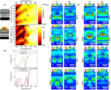
[image:6.595.108.490.90.400.2]vertical cross section (x–z plane) through one unit cell of hybrid structures with polymer thicknesses of 100 nm, 280 nm, 180 nm and 380 nm. Comparing the electric and magnetic field distributions for the hybrid nanostructures with 100 nm and 280 nm polymer thickness in Figure 2c, one notices that the local field distributions are extremely similar, although the polymer thicknesses is increased substantially. The electric fields (at 585 nm/575 nm and at 625 nm) for the nanostructure with 100 nm and 280 nm polymer thickness are stronger at the nanodisc polymer interface than at the nanodisc air interface. The electric fields exhibit multipolar character so that the coupling to the far field is extremely weak. Moreover, the magnetic fields at 585 nm/575 nm are confined within the polymer layers, so that the light can be nearly completely trapped within the hybrid nanostructure. Consequently, the reflectance at 585 nm is minimal.
Figure 2. (a) Comparison of the reflectance of the back-reflector alone with the reflectance from the
Au nanodisc-Ag back-reflectorhybrid structure. The occurrence as well as absence of the spectrally narrow features at 585 nm and 625 nm are governed by the interaction of localized plasmonic modes of the nanodiscs with the thin film modes of the back-reflector. (b) Simulated reflectance spectra of the hybrid structures for polymer spacer thicknesses of 100 nm (1*), 280 nm (1#), 180 nm (2*) of 380
nm (2#). The spectra are displayed in the individual generated colours (sRGB). (c) Electric and
magnetic field distributions at 585 nm/575 nm and at 625 nm along the vertical cross section (x–z plane) through one unit cell of hybrid structures with polymer thicknesses of 100 nm and 280 nm. In our coordinate system, the plane wave excitation is normally incident from the airside of the nanostructure, i.e., k vector parallel to the z-axis, and p–polarized, polarization parallel to the x–axis. The black lines in the field maps indicate the gold nanodiscs, the air-polymer and the polymer silver interfaces. (d) Electric and magnetic field distributions at 625 nm and 585 nm along the vertical cross section through one unit cell of hybrid structures with polymer thicknesses of 180 nm and 380 nm.
In contrast, the reflectance is substantially higher at 625 nm, since the electric and magnetic fields couple now to the far field. At this wavelength, the reflectance seems dominated by the back-reflector mode, which at 625 nm exhibits a local maximum. Additionally, the electric and magnetic field amplitudes at 625 nm are smaller than at 585 nm, therefore the light trapping within the
Figure 2.(a) Comparison of the reflectance of the back-reflector alone with the reflectance from the Au nanodisc-Ag back-reflector hybrid structure. The occurrence as well as absence of the spectrally narrow features at 585 nm and 625 nm are governed by the interaction of localized plasmonic modes of the nanodiscs with the thin film modes of the back-reflector. (b) Simulated reflectance spectra of the hybrid structures for polymer spacer thicknesses of 100 nm (1*), 280 nm (1#), 180 nm (2*) of 380 nm (2#). The spectra are displayed in the individual generated colours (sRGB). (c) Electric and magnetic field distributions at 585 nm/575 nm and at 625 nm along the vertical cross section (x–z plane) through one unit cell of hybrid structures with polymer thicknesses of 100 nm and 280 nm. In our coordinate system, the plane wave excitation is normally incident from the airside of the nanostructure, i.e., k vector parallel to the z-axis, and p–polarized, polarization parallel to the x–axis. The black lines in the field maps indicate the gold nanodiscs, the air-polymer and the polymer silver interfaces. (d) Electric and magnetic field distributions at 625 nm and 585 nm along the vertical cross section through one unit cell of hybrid structures with polymer thicknesses of 180 nm and 380 nm.
In contrast, the reflectance is substantially higher at 625 nm, since the electric and magnetic fields couple now to the far field. At this wavelength, the reflectance seems dominated by the back-reflector mode, which at 625 nm exhibits a local maximum. Additionally, the electric and magnetic field amplitudes at 625 nm are smaller than at 585 nm, therefore the light trapping within the nanostructure is weaker. The hybrid nanostructures with 180 nm and 380 nm polymer thickness exhibit also very similar near-field distributions at the nanodisc air and air polymer interfaces (Figure2d). At 625 nm, the light is completely trapped within the hybrid nanostructure, since the electric fields exhibit multipolar character and the magnetic fields are mostly confined within the polymer layers. However, additional electromagnetic modes can be seen in both; the electric and the magnetic field distributions of the hybrid structure with a polymer thickness of 380 nm. We attribute these modes to the back reflector modes. The near field distributions Figure2c indicate that the re-occurrence of the spectrally sharp features also depends on the spatial separation of the localized nanosdisc modes with the local maxima and minima of the back reflector modes. The electric and magnetic field distribution at 585 nm reveal another aspect of the interactions between the back-reflector modes and the localized plasmon modes of the Au nanodiscs. As discussed previously, the back reflector modes exhibits a local maximum at around 585 nm for a 180 nm thick polymer film. Due to the interaction between the back reflector modes and the localized modes at 585 nm, the electric field distributions exhibit a dipolar character. Coupling to the far field is now facilitated, which results in a higher reflectance than at 625 nm.
The spectrally narrow feature at 585 nm is crucial for the generation of green colours, since the spectrally narrow feature overlaps with the maximum of the red CIE XYZ 2◦standard observer function z(λ) at 585 nm. The extremely low reflectivity compensates the maximum of z(λ). Moreover, for the generation of bright green colors, a high reflectance between 500 and 550 nm is desirable. At 545 nm, the back reflector modes are the main mechanism responsible for the relative high reflectivity. (c.f. Supplementary Materials for a detailed description of the main mechanisms responsible for the color generation). The spectral narrow feature at 585 nm does not occur, if the polymer thickness is below 80 nm or the Ag film is not present in the hybrid structure (c.f. Supplementary Materials). Green colours can be only generated with hybrid nanostructures with certain polymer thicknesses (above 80 nm), since the spectral narrow feature arises from both, the spectral and spatial overlap of the localized plasmonic modes of the nanodiscs and the local minima of the back reflector modes.
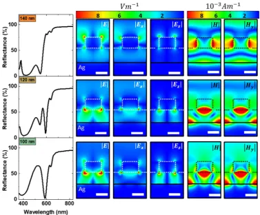
In order to get more insight into the origin of spectrally narrow feature at 585 nm, we now examine the electric and magnetic field distributions along the vertical cross section (x–z plane) through one unit cell of hybrid structures with polymer thicknesses of 140 nm, 120 nm and 100 nm (Figure3). The plane wave excitation is polarized along the x-axis and the k vector is parallel to the z direction, i.e., normal incidence. The white scale bars are 100 nm. The black line represents the polymer silver interface. For a polymer thickness of 140 nm, the hybrid nanostructures do not exhibit a spectrally narrow near–zero reflectance dip at 585 nm (Figure3left column, upper row). The electric field distributions for the nanostructure with 140 nm polymer thickness exhibit dipolar character, so that a coupling to the far-field is facilitated. Additionally, the total electric field as well as the Exand Ezfield components are stronger
Nanomaterials2019,9, 963 8 of 15
further reduced to 100 nm. In this case, the electric and magnetic fields are even more confined within the polymer layer, indicating efficient light trapping.
Nanomaterials 2019, 9, x FOR PEER REVIEW 7 of 15
[image:8.595.109.487.125.437.2]nanostructure is weaker. The hybrid nanostructures with 180 nm and 380 nm polymer thickness exhibit also very similar near-field distributions at the nanodisc air and air polymer interfaces (Figure 2d). At 625 nm, the light is completely trapped within the hybrid nanostructure, since the electric fields exhibit multipolar character and the magnetic fields are mostly confined within the polymer layers. However, additional electromagnetic modes can be seen in both; the electric and the magnetic field distributions of the hybrid structure with a polymer thickness of 380 nm. We attribute these modes to the back reflector modes. The near field distributions Figure 2c indicate that the re-occurrence of the spectrally sharp features also depends on the spatial separation of the localized nanosdisc modes with the local maxima and minima of the back reflector modes. The electric and magnetic field distribution at 585 nm reveal another aspect of the interactions between the back-reflector modes and the localized plasmon modes of the Au nanodiscs. As discussed previously, the back reflector modes exhibits a local maximum at around 585 nm for a 180 nm thick polymer film. Due to the interaction between the back reflector modes and the localized modes at 585 nm, the electric field distributions exhibit a dipolar character. Coupling to the far field is now facilitated, which results in a higher reflectance than at 625 nm.
Figure 3. Electric and magnetic field distributions at 585 nm along the vertical cross section (x-z plane)
through one unit cell of hybrid structures with polymer thicknesses of 140 nm, 120 nm and 100 nm. In our coordinate system, the plane wave excitation is normally incident from the air side of the nanostructure, i.e., k vector parallel to the z–axis, and p–polarized, polarization parallel to the x-axis. The black line in the field maps indicates the polymer silver interface. The white scale bar is 100 nm.
The spectrally narrow feature at 585 nm is crucial for the generation of green colours, since the spectrally narrow feature overlaps with the maximum of the red CIE XYZ 2° standard observer function z(λ) at 585 nm. The extremely low reflectivity compensates the maximum of z(λ). Moreover, for the generation of bright green colors, a high reflectance between 500 and 550 nm is desirable. At 545 nm, the back reflector modes are the main mechanism responsible for the relative high reflectivity. (c.f. Supplementary Materials for a detailed description of the main mechanisms
Figure 3. Electric and magnetic field distributions at 585 nm along the vertical cross section (x–z plane) through one unit cell of hybrid structures with polymer thicknesses of 140 nm, 120 nm and 100 nm. In our coordinate system, the plane wave excitation is normally incident from the air side of the nanostructure, i.e., k vector parallel to the z–axis, and p–polarized, polarization parallel to the x-axis. The black line in the field maps indicates the polymer silver interface. The white scale bar is 100 nm.
Nanomaterials2019,9, 963 9 of 15
responsible for the color generation). The spectral narrow feature at 585 nm does not occur, if the polymer thickness is below 80 nm or the Ag film is not present in the hybrid structure (c.f. Supplementary Materials). Green colours can be only generated with hybrid nanostructures with certain polymer thicknesses (above 80 nm), since the spectral narrow feature arises from both, the spectral and spatial overlap of the localized plasmonic modes of the nanodiscs and the local minima of the back reflector modes.
In order to get more insight into the origin of spectrally narrow feature at 585 nm, we now examine the electric and magnetic field distributions along the vertical cross section (x–z plane) through one unit cell of hybrid structures with polymer thicknesses of 140 nm, 120 nm and 100 nm (Figure 3). The plane wave excitation is polarized along the x-axis and the k vector is parallel to the z direction, i.e., normal incidence. The white scale bars are 100 nm. The black line represents the polymer silver interface. For a polymer thickness of 140 nm, the hybrid nanostructures do not exhibit a spectrally narrow near–zero reflectance dip at 585 nm (Figure 3 left column, upper row). The electric field distributions for the nanostructure with 140 nm polymer thickness exhibit dipolar character, so that a coupling to the far-field is facilitated. Additionally, the total electric field as well as the Ex and
Ez field components are stronger at the nanodisc air interface than at the nanodisc polymer interface.
[image:9.595.96.503.87.242.2]The magnetic field distribution reveals that although there is a strong field localisation between the nanodiscs, the magnetic field couples to the far-field as well. Consequently, the nanostructure exhibits a high reflectance at 585 nm in contrast to the nanostructures with 120 and 100 nm polymer thickness, respectively. Decreasing the polymer thickness to 120 nm leads to light trapping within the hybrid structure. Both, the electric and magnetic fields are now confined within the polymer layer. The field distributions in Figure 3 middle row show very strong localization of light under the nanodiscs. The electric field distribution does not show a dipolar character anymore. We attribute this together with the strong confinement of the magnetic field within the polymer as the major mechanisms responsible for the spectrally narrow near-zero reflectance dip at 585 nm which becomes more pronounced when the polymer thickness is further reduced to 100 nm. In this case, the electric and magnetic fields are even more confined within the polymer layer, indicating efficient light trapping.
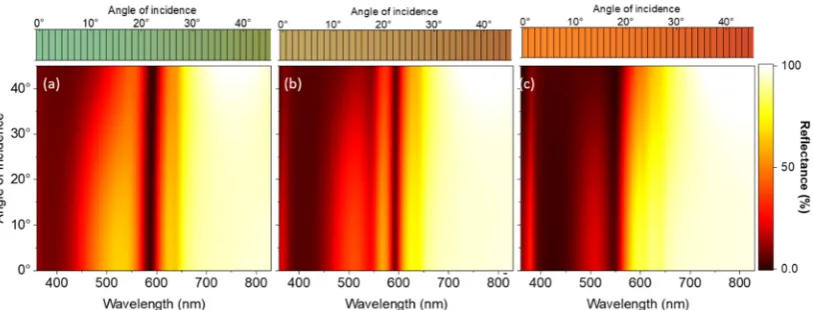
Figure 4. Simulated reflectance spectra as function of the illumination angle for hybrid structures with
polymer thicknesses of (a) 100 nm, (b) 120 nm and (c) 140 nm. The excitation was p-polarized. The calculated generated colours (sRGB) corresponding to the individual illumination angles are displayed above the simulated reflectance.
Since viewing angle insensitivity is highly desirable for structural color generation, we studied the angle-resolved optical response of our hybrid structure. This allows us to investigate in detail if the major mechanisms for structural color generation are due to localized modes or due to angular dispersive modes, such as propagating or diffractive modes. Viewing angle insensitivity implies that the color generation is mainly due to localized modes and that propagating and diffractive modes play only marginal roles. Figure 4 shows the calculated reflectance spectra and the generated colors as function of the angle of incidence for p-polarized excitation. Figure 4a shows the angular resolved
Figure 4. Simulated reflectance spectra as function of the illumination angle for hybrid structures with polymer thicknesses of (a) 100 nm, (b) 120 nm and (c) 140 nm. The excitation was p-polarized. The calculated generated colours (sRGB) corresponding to the individual illumination angles are displayed above the simulated reflectance.
Increasing the polymer thickness to 120 nm (Figure4b) leads to the near disappearance of the dispersive guided mode. The localized mode becomes spectrally sharper. For 140 nm polymer thickness the localized mode at 585 nm, and the guided mode observed in case of the 100 nm polymer thickness, do not exist. Instead, a spectrally blue shifted localized mode is observed at 550 nm. The color generation is mainly insensitive to the viewing angle.
Nanomaterials2019,9, 963 10 of 15
Nanomaterials 2019, 9, x FOR PEER REVIEW 9 of 15
reflectance of the hybrid structures with 100 nm polymer spacer thickness. Although such spectrally sharp features were previously observed in transmission due to hybridization of grating modes to propagating modes [68,69], here it is clear that the spectrally narrow mode at 585 nm is a localized mode and does not exhibit any angular dispersion. An angle dependent mode is observed in the blue spectral region (400–500 nm). We attribute this mode to the so-called guided mode [63]. The generated colors are barely influenced by the angle of incidence of the excitation, and hence the generated colors are not sensitive to the viewing angle. Figure S9 in the Supplementary Materials shows the reflectance spectra for different angles of incidence as well as optical band structure of a hybrid structure with 100 nm polymer thickness, i.e., the calculated reflectance as a function of the in–plane wavevector and energy for p-polarized excitation.
[image:10.595.182.417.88.328.2]Increasing the polymer thickness to 120 nm (Figure 4b) leads to the near disappearance of the dispersive guided mode. The localized mode becomes spectrally sharper. For 140 nm polymer thickness the localized mode at 585 nm, and the guided mode observed in case of the 100 nm polymer thickness, do not exist. Instead, a spectrally blue shifted localized mode is observed at 550 nm. The color generation is mainly insensitive to the viewing angle.
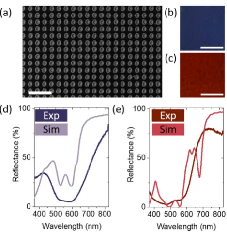
Figure 5. Experimental realisation: (a) SEM image of a representative nanodisc array (with 175 nm
diameter discs and 300 nm pitch). Scale bar is 1 μm. (b) and (c) Optical microscope images (at 100 × magnification) for the samples with polymer thicknesses of 70 nm and 196 nm, respectively. The white scale bars are 20 μm(d) and (e) Experimental and calculated reflectance spectra for polymer thicknesses of 70 nm and 196 nm, respectively. The spectra are presented in the corresponding sRGB colour.
We turn now our attention to the experimental realization of hybrid nanostructures to demonstrate the feasibility of facile fabrication of the versatile and robust two-metal component hybrid structures. In brief, a 100 nm thick silver film was deposited by evaporation on a silicon substrate. Subsequently, thin films of a propylene based polymer were spin coated on the silver film to form the back-reflector. 1 wt% and 2 wt% Tafmer in toluene stock solutions were used for the 70 nm and 196 nm thin polymer layer, respectively. In order to pattern the nanodisc arrays by electron beam lithography (EBL), a layer of ~250 nm positive tone resist (PMMA) was spin coated onto the polymer layer. After e-beam exposure, the array patterns were developed and a 100 nm thin gold layer was deposited by evaporation. Residual PMMA and gold was removed from the sample via lift-off leaving a 100 μm × 100 μm square array of nanodiscs with 175 nm diameter and 300 nm pitch.
Figure 5. Experimental realisation: (a) SEM image of a representative nanodisc array (with 175 nm diameter discs and 300 nm pitch). Scale bar is 1µm. (b,c) Optical microscope images (at 100× magnification) for the samples with polymer thicknesses of 70 nm and 196 nm, respectively. The white scale bars are 20µm (d,e) Experimental and calculated reflectance spectra for polymer thicknesses of 70 nm and 196 nm, respectively. The spectra are presented in the corresponding sRGB colour.
The experimental reflectance spectra, presented in Figure5d,e, were measured using a xenon lamp under normal incidence with a spot size of approximately 50µm in diameter. The spectra are presented in the corresponding sRGB color calculated from the experimental spectra, in excellent agreement with the observed color in the optical microscope images. For comparison, the calculated spectra for polymer thicknesses of 70 nm and 196 nm are shown in Figure5d,e, respectively. The simulated spectra are presented in the corresponding sRGB color. Overall, the simulations and experimental findings are in good agreement. The calculated colors are close to the experimental observations. However, the experimental spectra exhibit spectrally broader and less well defined features. This can be attributed mainly to variation in the thickness and surface roughness of the polymer layer, as well as to shape and size variation of the fabricated nanodiscs across the arrays. As discussed previously, the interaction of localized plasmonic modes of the nanodiscs with the thin film modes determines the occurrence of spectrally narrow features, i.e., the spectral and spatial overlap with the minima in reflectance of the back-reflector. The spectrally narrow feature observed at around 680 nm in Figure5e is strongly sensitive to changes in the spectral positions of the localized nanosdisc resonances, i.e., the red shifts of the resonances, as the disc diameter is increased (c.f. section 8 in the Supplementary Materials). Additionally, the area underneath the discs could have been overexposed during the e-Beam lithography, due to the close spacing of the nanoparticles. As a consequence, the nanodiscs could be embedded in the polymer. A possible optimization of the fabrication procedure involves minimizing the mentioned variations in the thickness of the polymer layer as well as variations in shape and in size of the fabricated nanodiscs across the arrays, i.e., using different polymers or polymer combinations for the polymer thin films.
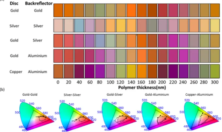
has limitations due to the d band absorption of gold below 520 nm, resulting in low reflectance at shorter wavelengths in the visible spectrum. Consequently, predominantly orange and red tones are generated. The CIE plot shows a concentration of chromaticity values in close proximity to the red trimulus value, occupying 13.56% of the sRGB triangle in the CIE chromaticity diagram. The red, green and blue primaries (corners of the sRGB triangle) represent the positions on the CIE colour-map that have the highest colour clarity. In order for a generated colour to be positioned in close proximity to one of these positions, the nanostructures must exhibit a substantial reflectance intensity in only one of the three colour cone regions of the visible spectrum, while having significantly smaller reflectance in the other two. The comparison of the occupied area on the CIE plot is a measure of distinction between colours in the colour palette, i.e., smaller area, means the colours are clustered, for example in the center of the CIE plot and hence, the color seem all a bit washed out.Nanomaterials 2019, 9, x FOR PEER REVIEW 11 of 15
Figure 6. (a) Generated colour as a function of polymer layer thickness for different metal disc and
back-reflector combinations. (b) CIE colour-space maps for each combination as a function of polymer thickness.
For a Ag-Ag system, the generated color palette consists entirely of pastel colors. The generated colors occupy 11.29% of the sRGB triangle in the CIE chromaticity diagram. Furthermore, this combination is less robust, since the Ag nanodiscs could easily tarnish, though the silver back-reflector is protected from the environment by the polymer layer. The Au-Ag hybrid metallic structure, discussed in detail above, produces a color palette which occupies 44.41% of the sRGB triangle in the CIE chromaticity diagram. To explore a cheaper alternative to the Au-Ag hybrid system, we propose to combine materials of lower cost. Aluminium exhibits high reflectance, comparable to Ag. The formation of a self-terminating 2 nm oxide layer protects the material from tarnishing [70], facilitating the fabrication. Replacing the Ag back-reflector with aluminum, produces a color palette with very similar properties to the Au-Ag hybrid metallic structure. However, the achievable color palette is slightly reduced, occupying 38.56% of the sRGB triangle. For the nanodisc material, Cu is an alternative to Au, since Cu nanodiscs exhibit resonances in the visible, at around 600 nm. The reflectance of Cu-Al hybrid structures show similarities to the reflectance of the Au-Ag structures, i.e., well-defined spectral features and high reflected intensity, corresponding to sRGB values with high color clarity (see Figure S15 in the Supplementary Materials). However, the observed modes in reflection are less spectrally sharp, since the plasmon resonances of both aluminium and copper are more damped compared to the plasmons of the more expensive Ag and Au materials. While the Al back–reflector–Cu nanodisc combination generates the largest color range, occupying 65.90% of the sRGB triangle, it must be kept in mind that copper oxidizes in ambient condition and encapsulation/protection of the copper nanodiscs would be necessary.
4. Conclusions
We have presented a hybrid metallic nanodisc back–reflector structure capable of producing vibrant color in reflection under white light illumination. The nanodiscs are separated from the continuous film back-reflector by a uniform polymer layer. This type of structure allows for the easy use of different metals for the nanodiscs and back–reflector. In the first instance Au nanodiscs separated from a Ag back-reflector were considered. FDTD simulations showed a large color gamut could be achieved as a function of the polymer film thickness with viewing angle insensitivity. Characterization of fabricated samples showed good agreement of the experimental reflectance spectra with the simulation data. A range of material combinations was investigated. The color
Figure 6. (a) Generated colour as a function of polymer layer thickness for different metal disc and back-reflector combinations. (b) CIE colour-space maps for each combination as a function of polymer thickness.
Nanomaterials2019,9, 963 12 of 15
be kept in mind that copper oxidizes in ambient condition and encapsulation/protection of the copper nanodiscs would be necessary.
4. Conclusions
We have presented a hybrid metallic nanodisc back–reflector structure capable of producing vibrant color in reflection under white light illumination. The nanodiscs are separated from the continuous film back-reflector by a uniform polymer layer. This type of structure allows for the easy use of different metals for the nanodiscs and back–reflector. In the first instance Au nanodiscs separated from a Ag back-reflector were considered. FDTD simulations showed a large color gamut could be achieved as a function of the polymer film thickness with viewing angle insensitivity. Characterization of fabricated samples showed good agreement of the experimental reflectance spectra with the simulation data. A range of material combinations was investigated. The color palette could be extended with nanostructures comprising two plasmonic materials. The colors generated by structures combining two different plasmonic materials occupy in-between∼40% and∼66% of the sRGB triangle in the CIE chromaticity diagram, with the Al back-reflector-Cu nanodisc combination showing the largest color range, while the colors generated by nanostructures consisting of a sole plasmonic material cover less the 14% of the sRGB triangle.
Supplementary Materials: The following are available online athttp://www.mdpi.com/2079-4991/9/7/963/s1, Figure S1: Complex refractive index of the propylene-based polymer. Table S1: Calculated sRGB values of the generated colors for different polymer thicknesses. Figure S2: Calculated colour generation (sRGB) as a function of polymer thickness. Figure S3: Comparison of the reflectance of the back-reflector alone with the reflectance from the Au nanodisc-Ag back-reflector hybrid structure and the simulated reflectance spectra of the individual components for a polymer thickness of 100 nm. Figure S4: Comparison of the reflectance of the back-reflector alone with the reflectance from the Au nanodisc-Ag back-reflector hybrid structure and the simulated reflectance spectra of the individual components for a polymer thickness of 180 nm. Figure S5: Main mechanisms for the generation of red and orange colours. Figure S6: Main mechanisms for the generation of green colours. Figure S7: Main mechanisms for the generation of blue and violet colours. Figure S8: Left: The calculated reflectance spectra of the back reflector alone of the hybrid nanostructure and of a hybrid nanostructure with the Ag thin film as a back reflector. The generated colour are displayed as inset. Right: The electric and magnetic field distributions at 450 nm, 545 nm, 585 nm and 625nm. Figure S9: Reflectance spectra for different angles of incidence and optical band structure of the Au nanodisc-Ag back-reflector hybrid structure with 100 nm polymer thickness. Figure S10: Calculated colour generation (sRGB) for different nanodisc heights. Figure S11: Calculated reflectance spectra of nanodisc arrays for discs with 125 nm, 150 nm and 150 nm diameter. Figure S12: Comparison of the experimental (stars) and calculated colours (squares) in CIE Plot. Figure S13: Calculated reflectance spectra of nanodisc arrays for discs with diameters of 175 nm and 100 nm in height. The nanodiscs could be embedded in the polymer to some extent, due to overexposure. Figure S14 (a) Polymer thickness dependence and (b) Au nanodisc diameter dependence. Figure S15: Calculated colour generation (sRGB) by a Cu nanodisc-Al back-reflector hybrid nanostructure as a function of polymer thickness.
Author Contributions: K.W.: Investigation, Formal Analysis, Visualization and Writing—original draft. C.A.M.: Investigation, methodology and Formal Analysis. E.P.-V. and C.S.: Investigation and Formal Analysis. C.H.: Methodology, Formal Analysis, Visualization and Writing—review and editing. A.L.B.: Conceptualization, Supervision, Project Administration, Funding Acquisition and Writing—review and editing. All authors discussed the results and commented on the manuscript.
Funding:This work was supported by Science Foundation Ireland (SFI) under grant numbers 13/TIDA/12717 and 10/IN.1/12975. K.W. acknowledges a postgraduate research scholarship from the Irish Research Council (GOIPG/2013/851).
Acknowledgments:Mitsui Chemicals Group for supplying the propylene polymer material used.
Conflicts of Interest:The authors declare no conflict of interest.
References
1. Kumar, K.; Duan, H.; Hegde, R.S.; Koh, S.C.W.; Wei, J.N.; Yang, J.K.W. Printing colour at the optical diffraction limit.Nat. Nanotechnol.2012,7, 557–561. [CrossRef] [PubMed]
3. Kristensen, A.; Yang, J.K.W.; Bozhevolnyi, S.I.; Link, S.; Nordlander, P.; Halas, N.J.; Mortensen, N.A. Plasmonic colour generation.Nat. Rev. Mater.2016,2, 16088. [CrossRef]
4. Lee, S.Y.; Forestiere, C.; Pasquale, A.J.; Trevino, J.; Walsh, G.; Galli, P.; Romagnoli, M.; Negro, L.D. Plasmon-enhanced structural coloration of metal films with isotropic Pinwheel nanoparticle arrays.
Opt. Express2011,19, 23818–23830. [CrossRef] [PubMed]
5. Lee, T.; Jang, J.; Jeong, H.; Rho, J. Plasmonic- and dielectric-based structural coloring: From fundamentals to practical applications.Nano Converg.2018,5, 1. [CrossRef] [PubMed]
6. Lee, H.-S.; Yoon, Y.-T.; Lee, S.-S.; Kim, S.-H.; Lee, K.-D. Color filter based on a subwavelength patterned metal grating.Opt. Express2007,15, 15457–15463. [CrossRef]
7. Diest, K.; Dionne, J.A.; Spain, M. Tunable color filters based on metal–insulator–metal resonators.Nano Lett.
2009,9, 2579–2583. [CrossRef]
8. Yoon, Y.-T.; Lee, S.-S. Transmission type color filter incorporating a silver film based etalon.Opt. Express
2010,18, 5344–5349. [CrossRef]
9. Si, G.; Zhao, Y.; Lv, J.; Lu, M.; Wang, F.; Liu, H.; Xiang, N.; Huang, J.; Danner, A.; Teng, J.; et al. Reflective plasmonic color filters based on lithographically patterned silver nanorod arrays.Nanoscale2013,5, 6243–6248. [CrossRef]
10. Smith, A.F.; Skrabalak, S.E. Metal nanomaterials for optical anti-counterfeit labels.J. Mater. Chem. C2017,5, 3207–3215. [CrossRef]
11. Fan, J.R.; Wu, W.G. Metal-dielectric-metal plasmonic nanohelms as broad-color-gamut tunable pixels for vivid display. In Proceedings of the 29th International Conference on Micro Electro Mechanical Systems (MEMS), Shanghai, China, 24–28 January 2016.
12. Yokogawa, S.; Burgos, S.P.; Atwater, H.A. Plasmonic Color Filters for CMOS Image Sensor Applications.
Nano Lett.2012,12, 4349–4354. [CrossRef] [PubMed]
13. Chen, Q.; Chitnis, D.; Walls, K.; Drysdale, T.D.; Collins, S.; Cumming, D.R.S. CMOS Photodetectors Integrated with Plasmonic Color Filters.IEEE Photonics Technol. Lett.2012,24, 197–199. [CrossRef]
14. Kats, M.A.; Blanchard, R.; Genevet, P.; Capasso, F. Nanometre optical coatings based on strong interference effects in highly absorbing media.Nat. Mater.2012,12, 20–24. [CrossRef] [PubMed]
15. Kreibig, U.; Vollmer, M. Optical Properties of Metal Clusters; Springer: Berlin, German, 1995; ISBN 978-3-64-2081-910.
16. Maier, S.A. Plasmonics: Fundamentals and Applications; Springer: Berlin, Germany, 2007; ISBN 978-0-38-7378-251.
17. Maniyara, R.A.; Rodrigo, D.; Yu, R.; Canet-Ferrer, J.; Ghosh, D.S.; Yongsunthon, R.; Baker, D.E.; Rezikyan, A.; García de Abajo, F.J.; Pruneri, V. Tunable plasmons in ultrathin metal films.Nat. Photonics2019,13, 328–333. [CrossRef]
18. Yu, R.; Mazumder, P.; Borrelli, N.F.; Carrilero, A.; Ghosh, D.S.; Maniyara, R.A.; Baker, D.; García de Abajo, F.J.; Pruneri, V. Structural Coloring of Glass Using Dewetted Nanoparticles and Ultrathin Films of Metals.ACS Photonics2016,3, 1194–1201. [CrossRef]
19. Kelly, K.L.; Coronado, E.; Zhao, L.L.; Schatz, G.C. The optical properties of metal nanoparticles: The influence of size, shape, and dielectric environment.J. Phys. Chem. B2003,107, 668–677. [CrossRef]
20. Jain, P.K.; Lee, K.S.; El-Sayed, I.H.; El-Sayed, M.A. Calculated absorption and scattering properties of gold nanoparticles of different size, shape, and composition: Applications in biological imaging and biomedicine.
J. Phys. Chem. B2006,110, 7238–7248. [CrossRef] [PubMed]
21. Khlebtsov, B.N.; Khlebtsov, N.G. Multipole plasmons in metal nanorods: Scaling properties and dependence on particle size, shape, orientation, and dielectric environment. J. Phys. Chem. C2007,111, 11516–11527. [CrossRef]
22. Zeng, B.; Gao, Y.; Bartoli, F.J. Ultrathin Nanostructured Metals for Highly Transmissive Plasmonic Subtractive Color Filters.Sci. Rep.2013,3, 2840. [CrossRef]
23. Franklin, D.; Chen, Y.; Vazquez-Guardado, A.; Modak, S.; Boroumand, J.; Xu, D.; Wu, S.-T.; Chanda, D. Polarization-independent actively tunable colour generation on imprinted plasmonic surfaces.Nat. Commun.
2015,6, 7337. [CrossRef]
Nanomaterials2019,9, 963 14 of 15
25. Goh, X.M.; Ng, R.J.H.; Wang, S.; Tan, S.J.; Yang, J.K.W. Comparative Study of Plasmonic Colors from All-Metal Structures of Posts and Pits.ACS Photonics2016,3, 1000–1009. [CrossRef]
26. Cheng, F.; Gao, J.; Luk, T.S.; Yang, X. Structural color printing based on plasmonic metasurfaces of perfect light absorption.Sci. Rep.2015,5, 11045. [CrossRef] [PubMed]
27. Miyata, M.; Hatada, H.; Takahara, J. Full-color subwavelength printing with gap-plasmonic optical antennas.
Nano Lett.2016,16, 3166–3172. [CrossRef] [PubMed]
28. Tan, S.J.; Zhang, L.; Zhu, D.; Goh, X.M.; Wang, Y.M.; Kumar, K.; Qiu, C.-W.; Yang, J.K.W. Plasmonic Color Palettes for Photorealistic Printing with Aluminum Nanostructures.Nano Lett.2014,14, 4023–4029. [CrossRef] [PubMed]
29. Roberts, A.S.; Pors, A.; Albrektsen, O.; Bozhevolnyi, S.I. Subwavelength Plasmonic Color Printing Protected for Ambient Use.Nano Lett.2014,14, 783–787. [CrossRef] [PubMed]
30. Wang, H.; Wang, X.; Yan, C.; Zhao, H.; Zhang, J.; Santschi, C.; Martin, O.J.F. Full Color Generation Using Silver Tandem Nanodisks.ACS Nano2017,11, 4419–4427. [CrossRef] [PubMed]
31. Ye, M.; Sun, L.; Hu, X.; Shi, B.; Zeng, B.; Wang, L.; Zhao, J.; Yang, S.; Tai, R.; Fecht, H.-J.; et al. Angle-insensitive plasmonic color filters with randomly distributed silver nanodisks.Opt. Lett.2015,40, 4979–4982. [CrossRef] [PubMed]
32. Stewart, J.W.; Akselrod, G.M.; Smith, D.R.; Mikkelsen, M.H. Toward Multispectral Imaging with Colloidal Metasurface Pixels.Adv. Mater.2018,29, 1602971. [CrossRef]
33. Ellenbogen, T.; Seo, K.; Crozier, K.B. Chromatic Plasmonic Polarizers for Active Visible Color Filtering and Polarimetry.Nano Lett.2012,12, 1026–1031. [CrossRef]
34. Fang, B.; Yang, C.; Shen, W.; Zhang, X.; Zhang, Y.; Liu, X. Highly efficient omnidirectional structural color tuning method based on dielectric–metal–dielectric structure.Appl. Opt.2017,56, C175–C180. [CrossRef] [PubMed]
35. Goh, X.M.; Zheng, Y.; Tan, S.J.; Zhang, L.; Kumar, K.; Qiu, C.-W.; Yang, J.K.W. Three-dimensional plasmonic stereoscopic prints in full colour.Nat. Commun.2014,5, 5361. [CrossRef] [PubMed]
36. Olson, J.; Manjavacas, A.; Liu, L.; Chang, W.-S.; Foerster, B.; King, N.S.; Knight, M.W.; Nordlander, P.; Halas, N.J.; Link, S. Vivid, full-color aluminum plasmonic pixels. Proc. Natl. Acad. Sci. USA2014,111, 14348–14353. [CrossRef] [PubMed]
37. Wu, Y.-K.R.; Hollowell, A.E.; Zhang, C.; Guo, L.J. Angle-Insensitive Structural Colours based on Metallic Nanocavities and Coloured Pixels beyond the Diffraction Limit.Sci. Rep.2013,3, 1194. [CrossRef] [PubMed] 38. Gwyn, C.W.; Stulen, R.; Sweeney, D.; Attwood, D. Extreme ultraviolet lithography.J. Vac. Sci. Technol. B
Microelectron. Nanom. Struct.1998,16, 3142–3149. [CrossRef]
39. Xia, D.; Ku, Z.; Lee, S.C.; Brueck, S.R.J. Nanostructures and Functional Materials Fabricated by Interferometric Lithography.Adv. Mater.2011,23, 147–179. [CrossRef]
40. Zhang, J.; Ou, J.-Y.; Papasimakis, N.; Chen, Y.; MacDonald, K.F.; Zheludev, N.I. Continuous metal plasmonic frequency selective surfaces.Opt. Express2011,19, 23279–23285. [CrossRef]
41. Ebbesen, T.W.; Lezec, H.J.; Ghaemi, H.F.; Thio, T.; Wolff, P.A. Extraordinary optical transmission through sub-wavelength hole arrays.Nature1998,391, 667–669. [CrossRef]
42. Chen, Q.; Cumming, D.R.S. High transmission and low color cross-talk plasmonic color filters using triangular-lattice hole arrays in aluminum films.Opt. Express2010,18, 14056–14062. [CrossRef]
43. Miroshnichenko, A.E.; Flach, S.; Kivshar, Y.S. Fano resonances in nanoscale structures.Rev. Mod. Phys.2010,
82, 2257–2298. [CrossRef]
44. Shen, Y.; Rinnerbauer, V.; Wang, I.; Stelmakh, V.; Joannopoulos, J.D.; Soljaˇci´c, M. Structural Colors from Fano Resonances.ACS Photonics2015,2, 27–32. [CrossRef]
45. Chu, Y.; Crozier, K.B. Experimental study of the interaction between localized and propagating surface plasmons.Opt. Lett.2009,34, 244–246. [CrossRef] [PubMed]
46. Liu, N.; Mesch, M.; Weiss, T.; Hentschel, M.; Giessen, H. Infrared perfect absorber and its application as plasmonic sensor.Nano Lett.2010,10, 2342–2348. [CrossRef] [PubMed]
47. Zhou, F.; Liu, Y.; Cai, W. Huge local electric field enhancement in hybrid plasmonic arrays.Opt. Lett.2014,
39, 1302–1305. [CrossRef] [PubMed]
49. Nicolas, R.; Lévêque, G.; Marae-Djouda, J.; Montay, G.; Madi, Y.; Plain, J.; Herro, Z.; Kazan, M.; Adam, P.-M.; Maurer, T. Plasmonic mode interferences and Fano resonances in metal-insulator-metal nanostructured interface.Sci. Rep.2015,5, 14419. [CrossRef]
50. Xiong, K.; Tordera, D.; Emilsson, G.; Olsson, O.; Linderhed, U.; Jonsson, M.P.; Dahlin, A.B. Switchable Plasmonic Metasurfaces with High Chromaticity Containing Only Abundant Metals.Nano Lett.2017,17, 7033–7039. [CrossRef]
51. Choi, D.; Shin, C.K.; Yoon, D.; Chung, D.S.; Jin, Y.W.; Lee, L.P. Plasmonic Optical Interference.Nano Lett.
2014,14, 3374–3381. [CrossRef]
52. Chen, Y.; Duan, X.; Matuschek, M.; Zhou, Y.; Neubrech, F.; Duan, H.; Liu, N. Dynamic Color Displays Using Stepwise Cavity Resonators.Nano Lett.2017,17, 5555–5560. [CrossRef]
53. Xiong, K.; Emilsson, G.; Maziz, A.; Yang, X.; Shao, L.; Jager, E.W.H.H.; Dahlin, A.B. Plasmonic Metasurfaces with Conjugated Polymers for Flexible Electronic Paper in Color.Adv. Mater.2016,28, 9956–9960. [CrossRef] 54. Cai, W.; Chettiar, U.K.; Yuan, H.-K.; de Silva, V.C.; Kildishev, A.V.; Drachev, V.P.; Shalaev, V.M. Metamagnetics
with rainbow colors.Opt. Express2007,15, 3333–3341. [CrossRef] [PubMed]
55. Fang, Z.; Zhen, Y.-R.; Fan, L.; Zhu, X.; Nordlander, P. Tunable wide-angle plasmonic perfect absorber at visible frequencies.Phys. Rev. B2012,85, 245401. [CrossRef]
56. Kim, W.; Simpkins, B.S.; Long, J.P.; Zhang, B.; Hendrickson, J.; Guo, J. Localized and nonlocalized plasmon resonance enhanced light absorption in metal-insulator-metal nanostructures.JOSA B2015,32, 1686–1692. [CrossRef]
57. Pinton, N.; Grant, J.; Collins, S.; Cumming, D.R.S. Exploitation of Magnetic Dipole Resonances in Metal-Insulator-Metal Plasmonic Nanostructures to Selectively Filter Visible Light.ACS Photonics2018,5, 1250–1261. [CrossRef]
58. Zhang, B.; Zhao, Y.; Hao, Q.; Kiraly, B.; Khoo, I.-C.; Chen, S.; Huang, T.J. Polarization-independent dual-band infrared perfect absorber based on a metal-dielectric-metal elliptical nanodisk array.Opt. Express2011,19, 15221–15228. [CrossRef] [PubMed]
59. Zhang, B.; Hendrickson, J.; Guo, J. Multispectral near-perfect metamaterial absorbers using spatially multiplexed plasmon resonance metal square structures.J. Opt. Soc. Am. B2013,30, 656–662. [CrossRef] 60. Liu, B.; Tang, C.; Chen, J.; Yan, Z.; Zhu, M.; Sui, Y.; Tang, H. The coupling effects of surface plasmon polaritons
and magnetic dipole resonances in metamaterials.Nanoscale Res. Lett. 2017,12, 586. [CrossRef] [PubMed] 61. Palik, E.D.Handbook of Optical Constants of Solids; Academic Press: New York, NY, USA, 2012.
62. Babar, S.; Weaver, J.H. Optical constants of Cu, Ag, and Au revisited.Appl. Opt.2015,54, 477–481. [CrossRef] 63. Zhou, W.; Suh, J.Y.; Hua, Y.; Odom, T.W. Hybridization of Localized and Guided Modes in 2D
Metal–Insulator–Metal Nanocavity Arrays.J. Phys. Chem. C2013,117, 2541–2546. [CrossRef]
64. International Commission on Illumination. Colorimetry: Understanding the CIE System; Schanda, J., Ed.; International Commission on Illumination: Vienna, Austria, 2007; ISBN 978-0-47-0175-620.
65. Choudhury, R.; Kumar, A.Principles of Colour and Appearance Measurements; Woodhead Publishing: Cambridge, UK, 2014.
66. Reinhard, E.; Khan, E.; Akyüz, A.; Johnson, G.Color Imaging: Fundamentals and Applications; Peters, A.K., Ed.; CRC PRESS: Boca Raton, FL, USA, 2008; ISBN 978-1-56-8813-448.
67. Oleari, C. (Ed.)Standard Colorimetry; John Wiley & Sons, Ltd.: Chichester, UK, 2015; ISBN 978-1-11-8894-477. 68. Kaplan, A.F.; Xu, T.; Jay Guo, L. High efficiency resonance-based spectrum filters with tunable transmission
bandwidth fabricated using nanoimprint lithography.Appl. Phys. Lett.2011,99, 143111. [CrossRef] 69. Fleischman, D.; Sweatlock, L.A.; Murakami, H.; Atwater, H. Hyper-selective plasmonic color filters.
Opt. Express2017,25, 27386–27395. [CrossRef] [PubMed]
70. Langhammer, C.; Schwind, M.; Kasemo, B.; Zori´c, I. Localized surface plasmon resonances in aluminum nanodisks.Nano Lett.2008,8, 1461–1471. [CrossRef] [PubMed]