Highly efficient coupling between a monolithically integrated Photonic
Crystal Cavity and a Bus Waveguide
Kapil Debnath*
a, Karl Welna
a, Marcello Ferrera
a, Kieran Deasy
b, David Lidzey
b, Thomas F.
Krauss
a, Liam O’Faolain
aa
School of Physics and Astronomy, University of St Andrews, North Haugh, St Andrews, Fife,
KY16 9SS, Scotland, UK;
b
School of Physics and Astronomy, University of Sheffield, Sheffield, S3 7RH, UK
ABSTRACT
We experimentally demonstrate a new optical filter design comprising of a photonic crystal cavity and a low index bus waveguide which are monolithically integrated on a silicon-on-insulator (SOI) platform. We have fabricated oxide clad PhC cavities with a silicon nitride waveguide positioned directly above, such that there is an overlap between the evanescent tails of the two modes. We have realised an extinction ratio of 7.5dB for cavities with total Q of 50,000.
Keywords: Photonic crystal, cavity-waveguide coupling, WDM
1.
INTRODUCTION
Two-dimensional photonic crystals have attracted a lot of attention because of their ability to strongly confine light in both space and time by means of the photonic band gap effect1. The two dimensional geometry is compatible with standard semiconductor processes allowing 2D photonic crystal based devices such as waveguides2, light sources3,4,5and resonant cavities6,7,8,9 to be realized in a range of different platforms. Photonic crystal based resonant nanocavities are of particular interest for Wavelength Division Multiplexing, quantum electro dynamics and light sources because of their ultra-small mode volume and ultra-high quality factor6,7.
Wavelength division multiplexing has become an essential part of modern optical communication systems, maximizing the available bandwidth by transmitting multiple channels simultaneously through the same optical fiber using multiple wavelengths. In a WDM system, high Q nanocavity based filters can be used to multiplex and demultiplex closely spaced channels10. The low mode volume maximizes the integration density and allows very low power operation. There are two main coupling approaches used to achieve an efficient optical filter by means of a waveguide/photonic crystal cavity system; one is planar coupling8,9,11,12,13, such as in-line coupling and side coupling, where both the cavity and the waveguides are created from the same photonic crystal; and the other is fiber taper based coupling, where light is coupled from a vertically placed fiber taper to the cavity14,15,16 .
The planar coupling scheme offers the possibility of monolithic integration. However, the presence of waveguides in close proximity to a high Q cavity introduces additional k-vector components within the light cone of the cavity increasing the out-of-plane loss and reducing the overall quality factor8. As the coupling strength depends on the separation between the cavity and the waveguide, the planar coupling scheme has limited design flexibility because of the discrete separation between the waveguide and the cavity-decided by the period of the photonic crystal lattice. Additionally due to the use of a bus waveguide composed of a high refractive index material, there can be huge insertion losses due to a large index mismatch mode mismatch with an optical fiber. Inverse tapers17 and grating couplers18 have been used to reduce this loss; however this adds design and fabrication complexity or bandwidth limitations.
Vertical coupling using tapered fiber can alleviate some of these problems. This is a relatively simple technique in which the mode of the tapered fiber overlaps with that of the cavity allowing a wavelength power transfer15. However, there is still a strong refractive index mismatch the tapered fiber and the cavity limits the filtering/drop efficiency to less than 3dB14. There are several designs proposed to improve the coupling efficiency15,16, the drop efficiency remains insufficient for use in WDM systems for telecommunication. In addition, the mechanical stability of the fiber coupling approach is poor, limiting the potential applications.
In this paper we propose a novel design of an optical filter based on cavity-waveguide coupling system where a bus waveguide of low index material is vertically coupled to a photonic crystal cavity in the Silicon on insulator platform. A thin oxide layer separates the two layers, providing some control over the coupling strength and mechanical stability. This technique offers a high degree of design flexibility and can achieve large coupling efficiency in a monolithic system.
2.
DESIGN
The proposed vertical coupling scheme is shown in Figure 1. Here we consider that both the waveguide and the cavity are single mode in the wavelength range of interest. Hence under week-coupling approximation, the power transmission and reflection coefficient of the coupled waveguide-cavity system can be expressed as12
T =
2 cavity
2 2
o coupling cavity
(
)
(ω-ω )
(
)
(1)and
R =
2 coupling
2 2
o coupling cavity
(
)
(ω-ω )
(
)
. (2)Where, Γcavity (=ωo/2Qcavity) represents the intrinsic decay rate of the unloaded cavity and Γcoupling represents the cavity
decay rate in the presence of the waveguide. From the above equations it is obvious that at resonance (ω=ωo), T~0 and
[image:2.595.59.539.446.539.2]R~1, when Γcavity<< Γcoupling.
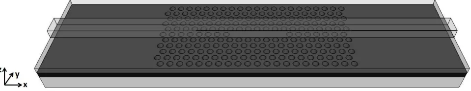
Figure 1. Schematic diagram of the proposed vertically coupled cavity waveguide system. A photonic crystal cavity on Silicon layer is coupled to a low index waveguide and separated by a thin layer of oxide.
In this vertical coupling approach it is possible to control Γcavity and Γcavity separately. To achieve a large unloaded quality
factor (i.e. small Γcavity) of the cavity we use a dispersion adapted (DA) Photonic-Crystal (PhC) Cavity that is designed to
confine the Gaussian mode profile in a gentle way. A W1 PhC waveguide is the basis of the cavity where we overlay an additional mode confinement in form of a potential well. The potential well is adapted to the dispersion curve of the PhC waveguide where its shape is recreated by laterally shifted holes. To do so, we use a dual-method, consisting of a (1) numerical plane-wave expansion method to simulate the dispersion curve and the cut-off frequencies for individual hole-shifts, and (2) an analytical formalism that allows to recreate the potential well by specifically shifted holes. The details of the cavity design will be presented elsewhere.
Γcoupling dependsmainly on two factors, a) spatial overlap of the evanescent modes of the cavity and the waveguide and b)
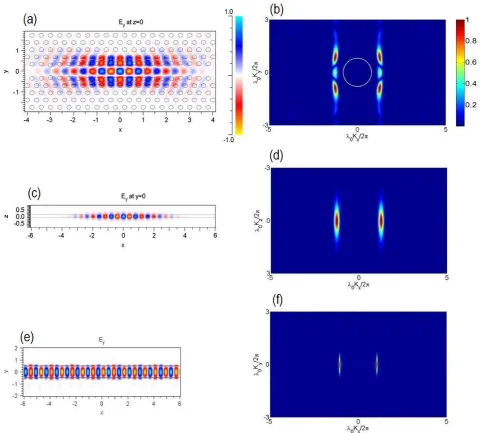
the barrier layer. As a result, the thickness of the barrier layer controls the degree of overlap between the evanescent tails of the two modes. And phase matching depends on the k-space overlap between the two modes. Figure 2a and 2b shows the real space field distribution and its Fourier transform of the dominant electric field Ey in the transverse (x-y) plane
respectively. Figure 2c and 2d shows the same in x-z plane. And Figure 2e and 2f shows the real space and Fourier transform of the Ey field in transverse plane for the waveguide. Since the Fourier components of the dominant field of
the cavity is centered about Kz = 0, phase matching will primarily depend on the overlap between the transverse Fourier
components of the waveguide and the cavity. Unlike in-plane coupling, vertically coupled waveguide does not alter the mode profile of the cavity significantly thus maintaining its high Q. Hence it is possible to position the waveguide very close to the cavity in order to achieve high extinction ratio.
[image:3.595.53.534.197.630.2]3.
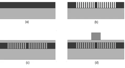
FABRICATION
The complete fabrication process19 is illustrated in Figure 3. A SOITEC silicon on insulator wafer with 220nm silicon with 2000nm buried oxide was spun with 400nm thick layer of an ebeam resist ZEP 520A. Using a hybrid ZEISS GEMINI 1530/RAITH ELPHY electron beam writer photonic crystal cavities were patterned into the resist at an acceleration voltage of 30KeV. The sample was then developed using Xylene and the pattern was transferred to the silicon layer via Reactive Ion Etching with SF6 and CHF3 gases at low power (20W) and low DC bias (-210V) to ensure
smooth side walls. Eventually the resist was cleaned using resist stripper 1165 and Piranha (3:1 H2SO4:H2O2). The
sample was then spun with a flowable oxide (FOx) containing hydrogen silsesquioxane (commercially available FOx-14 from Dow Corning). The sample was then baked at 100oC to remove the solvent and then hard baked at 400oC for four hours. The resulting oxide cladding had a thickness of 500nm. The oxide layer thickness was then reduced to 200nm by RIE with CHF3 gas, which was found to be the optimum thickness for efficient coupling while maintaining high Q. A
layer of silicon nitride was then deposited on the surface using plasma-enhanced chemical vapour deposition (PECVD). This was done using a Plasma-Therm 790 Series system, depositing the layer over a period of 45 minutes. After the deposition, the deposited layer was examined to verify the thickness and refractive index using an ellipsometer, where they were found to be 505nm and 1.88 respectively. The sample is then spun with ZEP 520A resist and waveguides with different width are patterned into the resist. The waveguide patterns were then transferred to the silicon nitride layer using reactive ion etching with CHF3 and O2 gases.
Figure 3. Fabrication process of the vertically coupled cavity-waveguide system, a) starting SOI wafer, b) Photonic crystal cavity patterns written into top silicon layer, c) Sample is cladded with FOx, c) Silicon nitride waveguide fabticated on top of the FOx layer.
4.
EXPERIMENTAL RESULTS
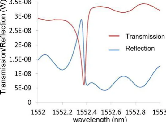
[image:4.595.63.540.301.561.2]shows a typical transmission and reflection spectra of the coupled cavity-waveguide system. At resonance, almost 80% of the light is reflected back and the overall quality factor is still maintained at 50000. From this results we can infer that Qcoupling ≈ 60000, and Qcavity ≈ 110000, where 1/ Qcavity = 1/ Qdesign + 1/ Qfabrication. And also due to the use of low index
[image:5.595.164.433.129.326.2]waveguides, the insertion loss is as low as 3dB, though it has been stated that loss can be as low as 0.05dB20.
Figure 4. Transmission and reflection spectra of the vertically coupled cavity waveguide system
5.
CONCLUSION
In this work an optical filter comprising of a vertically coupled cavity-waveguide system is proposed. Use of high-Q photonic crystal cavity offers an ultra-compact filter. This vertical coupling technique allows complete flexibility in choosing the cavity and waveguide design separately in order to achieve required Q and drop efficiency. We have experimentally found that an extinction ratio of 7.5dB can be achieved with a total Q of 50000 for a silicon nitride bus waveguide separated by a 200nm of oxide layer from the photonic crystal cavity.
REFERENCES
[1] Notomi, M., “Manipulating light with strongly modulated photonic crystals,” Rep. Prog. Phys. 73,(096501) (2010).
[2] Johnson, S. G., Villeneuve, P. R., Fan, S. and Joannopoulos, J. D., “linear waveguides in photonic-crystal slabs,” Phy. Rev. B 62, 8212-8222 (2000).
[3] Painter, O., Lee, R. K., Yariv, A., Scherer, A., O’Brien, J. D., Dapkus, P.D. and Kim, I., ‘‘Two-dimensional photonic band-gap defect mode laser,’’ Science 284, 1819–1824 (1999).
[4] Noda, S., Fujita, M. and Asano, T., “Spontaneous-emission control by photonic crystals and nanocavities,” Nature Photonics 1, 449 - 458 (2007)
[5] Altug, H., Englund, D. and Vu kovi , J., “Ultrafast photonic crystal nanocavity laser,” Nature Phys. 2, 484– 488 (2006).
[6] Song, B.-S., Noda, S., Asano, T. and Akahane, Y., “Ultra-high-Q photonic double-heterostructure nanocavity,” Nature Mater. 4, 207–210 (2005).
[7] Kuramochi, E., Notomi, M., Mitsugi, S., Shinya, A., Tanabe, T. and Watanabe, T., “Ultrahigh-Q photonic crystal nanocavities realized by the local width modulation of a line defect,” Appl. Phys. Lett. 88, 041112 (2006).
[9] Fan, S., Villeneuve, P., Joannopoulos, J. D. and Haus, H., “Channel drop filters in photonic crystals,” Optics Express 3, 4-11 (1998)
[10]Chen, L., Preston, K., Manipatruni, S., and Lipson, M., “Integrated GHz silicon photonic interconnect with micrometer-scale modulators and detectors,” Optics Express 17, 15248-15256 (2009)
[11]Joannopoulos, J. D., Johnson, S. G., Winn, J. N. and Meade, R. D., [Photonic crystals: molding the flow of light], 2nd Ed. Princeton University Press, Princeton, NJ (2008).
[12]Xu, Y., Li, Y., Lee, R. K., and Yariv, A., “Scattering-theory analysis of waveguide-resonator coupling,” Physical Review E 62, 7389-7404 (2000)
[13]Manolatou, C., Khan, M.J., Fan, S., Villeneuve, P.R., Haus, H.A., Joannopoulos, J. D., “Coupling of modes analysis of resonant channel add-drop filters,” IEEE J. Quantum Elect. 35, 1322 – 1331 (1999).
[14]Srinivasan, K., Barclay, P. E., Borselli, M. and Painter, O., “Optical-fiber-based measurement of an ultrasmall volume high-Q photonic crystal microcavity,” Phys. Rev. B 70, 081-306 (2004)
[15]Hwang, I. K., Kim, G.-H. and Lee, Y.-H., “Optimization of Coupling Between Photonic Crystal Resonator and Curved Microfiber,” IEEE J. Quatnum Electc. 42, 131-135 (2006)
[16]Hwang, I. K., “Modified linear photonic crystal resonator for efficient evanescent coupling to a tapered optical fiber,” J. Kor. Phys. Soc. 47, 434–438, 2005.
[17]Notomi, M., Shinya, A., Mitsugi, S., Kuramochi, E. and Ryu, H., “Waveguides, resonators and their coupled elements in photonic crystal slabs,” Optics Express 12, 1551-1561 (2004)
[18]Vermeulen, D., Selvaraja, S., Verheyen, P., Lepage, G., Bogaerts, W., Absil, P., Van Thourhout, D. and Roelkens, G., “High-efficiency fiber-to-chip grating couplers realized using an advanced CMOS-compatible Silicon-On-Insulator platform,” Optics Express 18, 18278-18283 (2010)
[19]White, T. P., O'Faolain, L., Li, J., Andreani, L. C. and Krauss, T. F., “Silica-embedded silicon photonic crystal waveguides,” Optics Express 16, 17076-17081 (2008)