Verification of band offsets and electron effective masses in GaAsN/GaAs quantum
wells: Spectroscopic experiment versus 10-band k·p modeling
K. Ryczko, G. Sk, P. Sitarek, A. Mika, J. Misiewicz, F. Langer, S. Höfling, A. Forchel, and M. Kamp
Citation: Journal of Applied Physics 113, 233508 (2013); doi: 10.1063/1.4810920
View online: http://dx.doi.org/10.1063/1.4810920
View Table of Contents: http://scitation.aip.org/content/aip/journal/jap/113/23?ver=pdfcov
Verification of band offsets and electron effective masses in GaAsN/GaAs
quantum wells: Spectroscopic experiment versus 10-band k
p modeling
K. Ryczko,1G. SeRk,1P. Sitarek,1A. Mika,1J. Misiewicz,1F. Langer,2S. Hofling,€ 2
A. Forchel,2and M. Kamp2
1
Institute of Physics, Wroclaw University of Technology, Wybrzeze Wyspia_ nskiego 27, 50-370 Wroclaw,
Poland
2
Technische Physik, Physikalisches Institut and Wilhelm-Conrad-R€ontgen-Research Center for Complex Material Systems, University of W€urzburg, Am Hubland, D-97074 Wurzburg, Germany€
(Received 1 March 2013; accepted 29 May 2013; published online 19 June 2013)
Optical transitions in GaAs1xNx/GaAs quantum wells (QWs) have been probed by two
complementary techniques, modulation spectroscopy in a form of photoreflectance and surface photovoltage spectroscopy. Transition energies in QWs of various widths and N contents have been compared with the results of band structure calculations based on the 10-band kp
Hamiltonian. Due to the observation of higher order transitions in the measured spectra, the band gap discontinuities at the GaAsN/GaAs interface and the electron effective masses could be determined, both treated as semi-free parameters to get the best matching between the theoretical and experimental energies. We have obtained the chemical conduction band offset values of 86% for x¼1.2% and 83% for x¼2.2%, respectively. For these determined band offsets, the electron effective masses equal to about 0.09 moin QWs with 1.2% N and 0.15 mofor the case of larger N
content of 2.2%.VC 2013 AIP Publishing LLC. [http://dx.doi.org/10.1063/1.4810920]
I. INTRODUCTION
Dilute nitride alloys such as GaAsN have attracted a great deal of experimental and theoretical attention in the last decade due to their unusual physical properties. One example is a drastically reduced bandgap with the incorpora-tion of a small amount of nitrogen into GaAs.1,2 This fact made these materials technologically attractive for opto-electronic devices,3–5 e.g., GaAsN was used in structures designed for fast saturable absorber devices.6 Moreover, GaAsN is very often used in more complex step-like quan-tum well (QW) structures as InGaAsN/GaAsN/GaAs, when it serves as a strain reducing layer and helps to reach longer emission wavelengths at lower In and N contents, which is beneficial for the structural and optical material quality, and hence also for the performances of the related devices.7,8In that context, such GaAsN-containing QWs can also be imag-ined to be exploited in more sophisticated and futuristic structures as QWs in optical resonators, where the physical effects resulting from a manipulation of both electronic and photonic wave functions can be used to tailor the light-matter interaction in the sense of coupling between the QW excitons and the photonic modes of the optical cavity. The latter, when combined with the use of dilute nitrides, could bring to the practical exploitation of the well-known polari-tonic physics and Bose-Einstein condensation in optoelec-tronic devices at the telecommunication wavelengths. As we have previously shown theoretically,9the oscillator strength of an InGsAsN/GaAsN/GaAs well, which can be used for the formation of exciton-polaritons at for instance 1.3lm, is strongly and non-monotonically dependent on the value of the band gap discontinuity (and hence the related band off-sets ratio) at the GaAsN/GaAs interface. Therefore, experi-mental determination or verification of the real band offsets
for this combination of materials is a subject of the current paper. We recognize that the existing literature data concern-ing that aspect seems to be inconsistent or controversial. Theoretical studies based on the dielectric model predicted a type-II alignment for the GaNAs/GaAs system,10 which has further been supported by X-ray photoemission spectros-copy,11 while first-principles calculations suggest a type-I lineup in this system,12with several following papers claim-ing that experimentally.13–17 Furthermore, adding nitrogen atoms into the GaAs matrix results in an enhancement of the electron effective mass, which makes the entire physical situation more complex and the proper interpretation of the optical spectra even more difficult. The issue of the effective mass has already been considered both theoretically and experimentally;16,18–22 however, currently the experimental results on the effective electron mass, especially in the case when the nitrogen (N) mole fraction approaches or exceeds 1.5% in the GaAsN layers,20are still significantly different than predicted from the band-anticrossing (BAC) modeling18 and certain corrections need to be considered.
In this report, we studied experimentally the energies of the interband transitions in GaAsN/GaAs QWs of various widths and compositions, and then identified them theoreti-cally exploiting the 10-band kp model, which allowed estimating both the band offset and the electron effective masses for N contents useful in photonic QW structures emitting in the telecommunication range of 1.3lm.
II. EXPERIMENTAL
For these studies, we used samples of GaAs1xNx/GaAs
single QWs grown by molecular beam epitaxy on a (001) GaAs substrate and a GaAs buffer, and capped with 100 nm of GaAs. There have been investigated two sets of structures
with two different N contents (1.2% and 2.2% of nitrogen) and various QW widths of 6, 8, and 10 nm. The compositions of the layers are determined based on growth calibration samples. At first the N content was calibrated by bulk-like GaAsN material. The relative strain of the given composition with respect to the GaAs substrate was estimated by high resolution X-ray diffraction (HR XRD), giving a direct mea-sure of the absolute N content. By using the same parameters again for the growth of the QW samples their composition could be given quite exactly. The estimated error bar is about 0.1% of the N content. The thicknesses of the QWs were calibrated in the same manner by accurately estimating the gallium growth rate by HR-XRD and double checking it with scanning electron microscopy measurements.
For the determination of the optical transitions, espe-cially the higher order ones which are more sensitive to the material parameter details like the band gap discontinuities, we used two different absorption like techniques, photoreflec-tance—PR (a kind of modulation spectroscopy) and surface photovoltage spectroscopy—SPS, both known as efficient in detecting the entire spectrum of transitions in various, even complex and multilayered, quantum structures.23–27 In photoreflectance (or modulated reflectivity) the normalized changes of the reflectivity coefficient are measured under external modulation stemming from varying illumination with a secondary beam (usually from a laser). This gives the derivative-like spectra with enhanced sensitivity to the optical transitions occurring in the investigated structure, of even a very small oscillator strength (as the nominally parity forbidden transitions, or those in quantum dots).28–30 Photoreflectance was measured by using a standard setup in the so called bright configuration31 when the tungsten halogen lamp and the 660 nm line of a semiconductor laser served as sources of the probe and pump beams, respec-tively. The photomodulated changes in the intensity of the reflected beam were detected by an InGaAs thermoelectri-cally cooled photodiode combined with a 0.5 m focal length monochromator dispersing the reflected light. The lock-in technique was used for the AC/DC signal processing and analog/digital conversion in order to record the spectral dependence of the normalized changes of the reflectivity coefficientDR/R.
In surface photovoltage spectroscopy, the change in the surface potential due to the optically excited electron–hole pair generation under periodic illumination and subsequent carrier redistribution and/or capture in the surface states are measured. For confined state structures as QWs, it basically reflects spectrally the absorption coefficient.23 Surface pho-tovoltage spectroscopy measurements were performed on an independent setup in a normal incidence beam configuration. The signal was measured between the sample and a reference metal grid electrode in a capacitive manner as a function of the photon energy of the probe beam. A soft contact mode was used to enhance the photovoltage signals.32The illumi-nation system consisted of a 200 W quartz-halogen lamp chopped at 180 Hz and a 0.3 m focal length grating mono-chromator. The photovoltage spectrum on the metal grid was measured with a copper plate as the ground electrode using a buffer circuit.
III. THEORETICAL APPROACH
To study the band structure of III–V semiconductor such as GaAsN we employed the kpmethod.33The strong inter-action between the N resonant states and the conduction band states means that the conventional 8-band kp model is not able to describe the band structure properly, especially the conduction band states of GaAsN/GaAs quantum wells. On the other hand, it has also been demonstrated that exploiting a simplified approach taking into account just the coupling between the conduction band states and the nitrogen states (so called band anticrossing model) is not satisfactory as well. It neglects the conduction and valence band interaction and does not give an accurate prediction of electron and hole higher energy confined states,34 whereas the latter are used by us for comparison with the experimental results. Therefore, this leads to the necessity of using the 10-bandkp
Hamiltonian, which we used after Ref. 33. We solved the Schr€odinger equation using the finite difference technique.35 The material parameters used in our calculations, except for band offsets and electron effective masses which are to be determined here, are taken after Ref.16. Further details of the used theoretical approach are described in the appendix.
IV. RESULTS AND DISCUSSION
A. Optical spectra
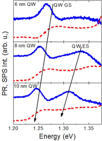
[image:3.612.351.523.476.712.2]In order to verify the band structure details as, e.g., the band offsets, we have used two complementary experimental techniques, both giving absorption-like spectra. These spec-tra allow for a highly sensitive detection of optical spec-transitions in low-dimensional structures.23–27,36 Figure 1 shows an example of such room temperature spectra for three GaAsN/ GaAs QW samples with the nominal N content of about
FIG. 1. Room temperature photoreflectance (solid blue lines) and surface photovoltage spectroscopy spectra (red dashed lines) for three GaAs0.988N0.012/GaAs QWs of different widths. The spectral features are
assigned as QW GS and QW ES for the ground and excited state optical transitions, respectively.
1.2% and different QW widths of 6, 8, and 10 nm. Using var-ious widths for a constant composition is an approach which allows probing the appearance/disappearance of higher order state transitions in the spectra (due to the changed confine-ment width, the number of confined levels is altered), which eventually, after comparing to the results of calculations, allows determining the band gap discontinuities (only the proper discontinuity will give the agreement for the transi-tion energies, and especially the number of confined state transitions for various QW widths). As can be seen in Fig.1, there is only one spectral feature present for the narrowest QW (6 nm width), in both types of spectra, PR and SPS. This, even without the calculations, can be attributed to the fundamental transition in the well. This transition is observed for the wider QWs and shifts to the red with increasing the width, as expected. For the 8 nm wide QW, a second feature appears at about 80 meV higher energy. And finally, this sec-ond transition is also observed for the case of the 10 nm wide QW, being red shifted and separation of which decreased to about 60 meV with respect to the ground state transition, i.e. as expected with increasing the well layer thickness. It is worth noting that no other optical features could be observed, except of the GaAs-related bulk-like transition, which has been left out of the range of Fig.1for clarity (as this is much more intensive, and out of the interest for this discussion). In order to derive more exact spectral positions of the observed features, a respective analysis must be employed. In the case of the PR spectra (whose line shape is derivative-like), a fitting procedure according to the follow-ing formula has been performed:
DR
R ðEÞ ¼Re½Ce i#ð
EE0þiCÞm; (1)
whereCand# are the amplitude and phase of the spectral line, andE0andCare the energy and the broadening
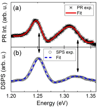
param-eter of the transition, respectively. The paramparam-eter m refers to the type of an optical transition and critical point. We used here m¼3 as it has been proven to produce a line shape imitating well the first derivative of Gaussian function (appropriate for inhomogeneously broadened confined state transitions) and giving correct transition energies. An exam-ple of such fit is shown in Fig.2(a)for the case of the 10 nm wide QW from Fig. 1. As the detailed line shape is also dependent on the phase parameter, the obtained energies, which are 1.253 and 1.328, respectively, fall spectrally between the two maxima of the respective PR lines.
Similarly, the extraction of the transition energy directly from the SPS spectra is not very exact, especially for the higher energy transitions, which appear on the background of the absorption related to the fundamental one, and are not very pronounced (however visible) in the spectrum as meas-ured (see Fig.1). Therefore, the processing of the spectra is needed, and a respective fitting procedure afterwards. It has been shown23,32 that the numerically calculated derivative of ESPSðEÞ with respect to the photon energy E, dðESPSðEÞ=dE(denoted as DSPS, i.e., a derivative of the SPS response) is proportional todðaðEÞÞ=dE, whereais the absorption coefficient and resembles the line shape described by Eq. (1) but for parameter m¼2. Such an analysis has
been used and its result is shown in Fig.2(b). As the phase parameter is by the definition different in the case of these spectra and the PR ones, the obtained energies, which are very close to the ones from PR (1.251 and 1.323 eV), fall more onto the respective peaks of the derivative curve of the DSPS signal. The second higher energy transition is also a bit less pronounced in DSPS, but generally, both the types of the spectra confirm the existence and the energy positions of the observed optical transitions.
Analogous spectra have also been recorded and their analysis performed for the second series of structures with 2.2% of nitrogen.
B. Band offset
The experimental data of the previous chapter is com-pared with the results of calculations within the theoretical model presented in Sec. III. We calculated the transition energies in GaAs1xNx/GaAs QWs with N contents of
x¼1.2% and 2.2%, and versus the well width in the range of at least 6–10 nm. The chemical band offsets (band gap dis-continuities), i.e., the ones between the unstrained materials (or before the application of the strain), are the input parame-ters, and treated as semi-free, i.e., tunable in order to match the theoretical dependencies with the experimental data. Figure 3compares the experimentally determined transition energies of a series of GaAs1xNx/GaAs QWs with x¼1.2%
[image:4.612.340.536.60.275.2]closer to 70% or 90%. As we see, indeed an unambiguous determination of the band offset is hardly possible when fol-lowing just the ground state transition, which is weakly sen-sitive to that parameter of the structure. Additionally, which should be expected in the case of these tensile strained QWs, there coexist two closely spaced transitions in the range of the lowest energy spectral feature: a light hole related transi-tion (i.e. between the fundamental light hole confined level and fundamental electron confined level—lh1-e1) and at slightly higher energy a heavy hole transition (the fundamen-tal heavy hole confined level and the fundamenfundamen-tal electron confined level—hh1-e1). While considering only the transi-tions at k¼0, we can still use the names as in the single band model, i.e., “heavy hole” or “light hole” bands. The superposition of the two transitions at the ground state energy makes the interpretation even more difficult, espe-cially as these two transitions are separated by only a few meV and cannot be resolved in the broadened spectra (the line broadening is about 20 meV) of rather strongly inhomo-geneous system of dilute nitride. However, one can assume that the experimental spectra are mostly dominated by the heavy hole transitions having larger oscillator strength (by approximately a factor of 3 in the quantum well).
The higher order transitions change much stronger when the band offsets are altered and the “lh” and “hh” ones are better separated. When analyzing the dependencies plotted in Fig. 3, we observe that the calculated hh2-e2 transition (second heavy hole level and second electron level) occurs very close to the energies of the experimental higher energy spectral feature (called QW ES in Fig.1). Although the abso-lute energies do not agree very exactly, one can still follow the tendency and number of transitions expected in the spec-tra. The latter brings us to the conclusion that the conduction band offset must be taken from the range of 80%–90% for N content of 1.2%, because for 80% or smaller values a second
optical transition should also be present in the spectra for the 6 nm wide QW, which is not the case. On the other hand, the second transition could not be seen for the 8 nm wide QW, if the conduction band offset is 90%. This result remains in agreement with some of the previous considerations.16,21 Therefore, following the dependence proposed in Ref. 16, we obtain that the conduction band offsets could be about 86% for x¼1.2%. When analyzing similarly the data for the larger N content, and assuming the dependence from Ref.16 is still valid, we obtain the conduction band offset ratio of about 83% for x¼2.2%. These two offset values are then used in further calculations.
C. Electron effective mass
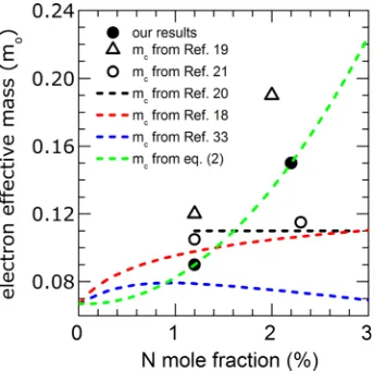
In order to improve the agreement between the theoreti-cal and experimental results, we tune the electron effective mass, which is the second parameter which is not very well defined in the literature. Figure4shows the calculated transi-tion energies in GaAs1xNx/GaAs QWs for two different N
mole fractions x¼1.2% (a) and x¼2.2% (b) as a function of the QW width. The red dashed lines show results obtained using the theoretical model presented in Ref. 33, while the black full dots correspond to our experimental results. In order to improve the agreement with respect to the experi-mental data, the transition energies have also been calculated for the corrected electron effective mass—solid black curves in Fig. 4. For the two considered cases of N content, the effective electron mass has been set to be equal to 0.09 mo
for the sample with 1.2% N and 0.15 mofor the sample with
2.2% N. In the second case, this is more than twice larger than the electron effective mass in GaAs. Suggestions on the necessity to increase the effective mass in GaAsN have al-ready been made in several papers previously.13,16,19–21,37 Hai and co-workers19 determined the mass values to be 0.12 mo and 0.19 mofor 7 nm GaAsxN1x/GaAs QWs with
x¼1.2% and 2%, respectively. Authors in Ref.20 studied samples with a similar nitrogen content of 1.2%<x<2.8% and different GaAsxN1x well widths from 3 to 9 nm and
showed an increase in the electron effective mass to about 0.11 mo. Also in Ref. 21, it has been indicated that for
FIG. 3. Well width dependence of the transition energies of GaAs0.988N0.012/GaAs quantum wells calculated by using the 10-bandkp
Hamiltonian if the electron effective mass is from BAC model (Ref.18). The red, blue, and green lines (solid—heavy hole transitions; dashed—light hole transitions) represent the calculated values if the conduction band offset are equal to 70%, 80%, and 90%, respectively.
FIG. 4. Well width dependence of the transition energies of GaAs0.988N0.012/GaAs (a) and GaAs0.978N0.022/GaAs (b) quantum well
cal-culated by using the 10-bandkpHamiltonian if the electron effective mass is from Ref.33(dashed red line) and if the electron effective mass is equal to 0.09 for x¼1.2% N (a) and 0.15 for x¼2.2% N (b) (solid black line).
x¼1.2% the electron effective mass is 0.105 mo and for
x¼2.3% it has a value of 0.115 mo. Finally, our results of
electron effective mass are a bit lower than those reported in Ref.13. The previously existing descriptions for the N mole fraction from 0% to 3% give the results presented in Fig.5. The red dashed line concerns the results calculated using the BAC model,18 while the black dashed line corresponds to the results obtained based on the model proposed in Ref.16. The calculated values of effective electron mass are increased compared to GaAs, but still lower than those directly measured or determined indirectly using the optical experiments. This discrepancy is especially significant for the N mole fraction larger than 2%. This is described in Ref.37, in which it has been found by theab initioLMTO (Linear Muffin Tin Orbital) calculations that the values obtained for the electron effective mass at the bottom of the conduction band should be in the range from 0.065 mo to
0.12 mofor 0.009<x<0.04. In our case, and based on the
comparison to the experimental results, we approximated the electron effective mass in a function of the N content by the following expression:
meðxÞ mo
¼boþb1xþb2x2; (2)
wherebo¼0:067;b1¼ 0:31; and b2¼185:6. However, some further work and additional and independent experi-ments are still needed to confirm such a dependence for more values of the N contents, also out of the range of com-positions considered here.
V. SUMMARY
In summary, detecting the optical transitions in the GaAs1xNx/GaAs quantum wells by photoreflectance and
surface photovoltage spectroscopy has allowed studying the details of the band structure of this dilute nitride material system. The dependencies of the transition energies on the
well width and N concentration have been investigated. Based on the comparison of the experimental data with the results of the calculations from the 10-band kp modeling, we could estimate the conduction band offset to be equal 86% (64%) for x¼1.2% and 83% (63%) for x¼2.2%. The results suggest additionally an increase in the electron effec-tive mass to about 0.09mo for x¼0.012 and 0.15mo for
x¼0.022. Both the parameters need to be considered accordingly in order to predict properly on the electronic lev-els of more complex GaAs-based structures containing the GaAsN alloy. Eventually, the obtained band offset confirmed the expectations on the enhancement of the oscillator strength of the optical transitions in InGaAsN/GaAsN/GaAs QWs9designed to be employed for the formation of exciton polaritons in the telecommunication range. This makes the material system indeed promising for practical exploita-tion of the quantum-electrodynamics-based optoelectronic applications.
ACKNOWLEDGMENTS
The authors acknowledge the financial support from the bilateral project of Deutsche Forschungsgemeinschaft (Project named LIEPOLATE) and Polish Ministry of Science and Higher Education (Project No. DPN/N99/DFG/2010), and the COPERNICUS Award of the Foundation for Polish Science and Deutsche Forschungsgemeinschaft.
APPENDIX: TEN-BAND kp MODEL
In the 10-band scheme, the total wave function of the subbandnin the QW can be written as
WnðrÞ ¼ X10
j¼1
Fn;jðrÞujðrÞ;
whereFn,j(r) is the envelope function anduj(r) is the periodic part of the Bloch basis function at the zone center. The following Bloch basis functions for the high-lying N-band (N will be used to assign the nitrogen related states), the conduction band (CB), and the heavy hole (HH), the light hole (LH), and the spin-orbit split-off (SO) bands have been used to derive the 10-bandkpHamiltonian
ju1i ¼ 1 2;þ
1 2
¼ jsN;"i; (A1a)
ju2i ¼ 1 2;þ
1 2
¼ js;"i; (A1b)
ju3i ¼ 3 2;þ
3 2
¼ iffiffiffi
2
p ½jx;"i þijy;"i; (A1c)
ju4i ¼ 3 2;þ
1 2
¼ iffiffiffi
6
p ½jx;#i þijy;#i 2jz;"i; (A1d)
ju5i ¼ 1 2;þ
1 2
¼ iffiffiffi
3
[image:6.612.89.261.62.233.2]p ½jx;#i þijy;#i þ jz;"i; (A1e) FIG. 5. Effect of increasing N mole fraction on the electron effective mass.
Data points: experimental mass values taken from Ref.19(D), Ref.21(䊊), our results (䊉). The dashed black lines presents results from Ref.20. The dashed red line presents calculated values from BAC model (Ref.18). The dashed blue line presents results from Ref.33. The dashed green line, calcu-lated values with GaAs1xNx/GaAs QW electron effective mass given by
ju6i ¼ 1 2; 1 2
¼ jsN;#i; (A1f)
ju7i ¼ 1 2;þ
1 2
¼ js;#i; (A1g)
ju8i ¼ 3 2; 3 2
¼ iffiffiffi 2
p ½jx;#i ijy;#i; (A1h)
ju9i ¼ 3 2; 1 2
¼ þ iffiffiffi 6
p ½jx;"i ijy;"i þ2jz;#i; (A1i)
ju10i ¼ 1 2; 1 2
¼ þ iffiffiffi 3
p ½jx;"i ijy;"i jz;#i; (A1j)
wherejSNidenotes the s-like N Bloch state,jSidenotes the s-like CB Bloch state, and jxi;jyi;jzidenotes the p-like VB Bloch states. The 10-band kpHamiltonian, which includes the coupling of N, CB, HH, LH, and SO into account is given below
H¼
EN VNC 0 0 0 0 0 0 0 0
ECB
ffiffiffi 3 p
Tþ ffiffiffi2 p
U U 0 0 0 T ffiffiffi2
p T EHH ffiffiffi 2 p
S S 0 0 0 R pffiffiffi2R
ELH Q 0 Tþ R 0
ffiffiffi 3 p
S
ESO 0 ffiffiffi 2 p
Tþ pffiffiffi2R pffiffiffi3S 0
EN VNC 0 0 0
ECB ffiffiffi 3 p T ffiffiffi 2 p
U U
EHH
ffiffiffi 2 p
S S
ELH Q
ESO 2 6 6 6 6 6 6 6 6 6 6 6 6 6 6 6 6 6 6 6 4 3 7 7 7 7 7 7 7 7 7 7 7 7 7 7 7 7 7 7 7 5 ; where
EN ¼ENocxþjxþdEhydN ; (A2)
ECB¼ECoaxþjxþ
h2 2mo
sðkx2þk 2
yþk
2 zÞ þdE
hyd
CB; (A3)
EHH ¼Evoþjx
h2 2mo
ðc1þc2Þðk 2
xþk
2 yÞ
h 2
2mo
ðc12c2Þk2z þdE hyd
VB gax; (A4)
ELH¼EVoþjx
h2 2mo
ðc1c2Þðk 2
xþk
2 yÞ
h 2
2mo
ðc1þ2c2Þk 2 z þdE
hyd
VB þgax; (A5)
ESO¼EVoþjxDSO
h2 2mo
c1ðk 2
xþk
2
yÞ
h2 2mo
c1k 2 z
þdEhydVB; (A6)
T6¼ 1
ffiffiffi 6
p Pðkx6ikyÞ; (A7)
U¼ 1ffiffiffi 3
p Pkz; (A8)
S¼ ffiffiffi 3 2 r h2 mo
c3kzðkxikyÞ; (A9)
R¼ ffiffiffi 3 p 2 h2 2mo
½ðc2þc3ÞðkxikyÞ2 ðc3c2ÞðkxþikyÞ2;
(A10)
Q¼ 1ffiffiffi 2 p h
2
mo
c2k 2 jjþ
ffiffiffi 2 p h2
mo
c2k 2
z
ffiffiffi 2 p
gax; (A11)
k2jj¼k2xþky2; (A12)
and VN¼b ffiffiffix p
describes the coupling between the N states and conduction band edge, b is the interaction factor between N and CB, ENo, ECo, EVoare the energies of N, CB,
VB, respectively, DSO is the spin-orbit splitting energy, kx
and ky are the wave vectors in the plane, kz is the wave
vector along the QW growth direction. The term s¼1=mc ðEP=3Þ E2
gþ1=ðEgþDSOÞ
h i
is used in place of 1=mc. c1,
c2, and c3 are the modified Luttinger parameters
c1¼cL1EP=ð3EhgÞ,c2;3¼cL2;3EP=ð6EhgÞ. EP and Ehg are the optical matrix parameter and band gap of the host mate-rial, respectively. Pis the Kane matrix element for the con-duction band (EP ¼2moP2=h2). dEhydCB ¼ 2aið1cc12
11Þexx
and gax¼ baxð1þ2cc12
11Þexx describe the influence of the
hydrostatic and shear strain components on the band struc-ture, where ai are the hydrostatic deformation potentials (with index i¼N, CB, VB).c11 andc12 are the elastic con-stants, bax is the axial deformation potential and exx is the strain in the layer. The parametersaandbdescribe the band gap reduction due to the introduction of N, whilejtakes into account the variation of the VB offset between unstrained GaNxAs1xand GaAs. And finally,xis the fraction of N in
the structure. The band parameters of the parental binary compounds used in our calculations are taken after Ref.16.
We quantize the Hamiltonian along the growth direction (z-axis) and we replace the z component of k vector by the operator kz! i@=@z. Then, we denote the in-plane wave vector by kjj¼ ½kx;ky. We solve the 10-band kp Hamiltonian numerically using the finite difference technique.35
1M. Weyers, M. Sato, and H. Ando,Jpn. J. Appl. Phys.
31, L853–L855 (1992).
2
S.-H. Wei and A. Zunger,Phys. Rev. Lett.76, 664 (1996).
3J. W. Ager III and W. Walukiewicz,Semicond. Sci. Technol.17, 741 (2002). 4R. Oshima, A. Takata, and Y. Okada,Appl. Phys. Lett.
93, 083111 (2008).
5
D. Gollub, S. Moses, and A. Forchel, IEEE J. Quant. Elect. 40(4), 337–342 (2004).
6M. Le D^u, J.-C. Harmand, O. Mauguin, L. Largeau, L. Travers, and J.-L.
Oudar,Appl. Phys. Lett.88, 201110 (2006).
7
N. Tansu, J.-Y. Yeh, and Luke J. Mawst, Appl. Phys. Lett. 83, 2512 (2003).
8D. Bisping, D. Pucicki, M. Fischer, S. H€ofling, and A. Forchel,J. Cryst. Growth311, 1715 (2009).
9
K. Ryczko, G. SeRk, J. Misiewicz, F. Langer, S. H€ofling, and M. Kamp,
J. Appl. Phys.111, 123503 (2012).
10S. Sakai, Y. Ueta, and Y. Terauchi,Jpn J. Appl. Phys., Part 132, 4413
(1993).
11
T. Kitani, M. Kondow, T. Kikawa, Y. Yazawa, M. Okai, and K. Uomi,Jpn J. Appl. Phys., Part 138, 5003 (1999).
12L. Bellaiche, S.-H. Wei, and A. Zunger,Phys. Rev. B56, 10233 (1997). 13
Y. Zhang, A. Mascarenhas, H. P. Xin, and C. W. Tu,Phys. Rev. B61, 7479 (2000).
14
I. A. Buyanova, G. Pozina, P. N. Hai, W. M. Chen, H. P. Xin, and C. W. Tu,Phys. Rev. B63, 033303 (2000).
15P. Krispin, S. G. Spruytte, J. S. Harris, and K. H. Ploog,J. Appl. Phys.
90, 2405 (2001).
16
S. Tomic´, E. P. O’Reilly, P. J. Klar, H. Gruning, W. Heimbrodt, W. M. Chen, and I. A. Buyanova,Phys. Rev. B69, 245305 (2004).
17J.-R. Lee, Y.-Y. Chen, C.-R. Lu, W.-I. Lee, and S.-C. Lee, Mater. Sci. Eng. B100, 248 (2003).
18W. Walukiewicz, W. Shan, J. W. Ager III, D. R. Chamberlin, E. E. Haller,
J. F. Geisz, D. J. Friedman, J. M. Olson, and S. R. Kurtz, inProceedings of the 195th Electrochemical Society Meeting, Seattle, WA (The Electrochemical Society, Pennington, 1999), Vol. 99-11, p. 190.
19P. N. Hai, W. M. Chen, I. A. Buyanova, H. P. Xin, and C. W. Tu,Appl. Phys. Lett.77, 1843 (2000).
20
J. Wu, W. Shan, W. Walukiewicz, K. M. Yu, J. W. Ager III, E. E. Haller, H. P. Xin, and C. W. Tu,Phys. Rev. B64, 085320 (2001).
21R. Kudrawiec, M. Motyka, M. Gładysiewicz, J. Misiewicz, J. A. Gupta,
and G. C. Aers,Solid State Commun.138, 365 (2006).
22
T. Dannecker, Y. Jin, H. Cheng, C. F. Gorman, J. Buckeridge, C. Uher, S. Fahy, C. Kurdak, and R. S. Goldman,Phys. Rev. B82, 125203 (2010).
23S. Datta, B. M. Arora, and S. Kumar,Phys. Rev. B62, 13604 (2000). 24P. Sitarek, H. P. Hsu, Y. S. Huang, J. M. Lin, H. H. Lin, and K. K. Tiong,
J. Appl. Phys.105, 123523 (2009).
25
G. SeRk, M. Motyka, K. Ryczko, F. Janiak, J. Misiewicz, S. Belahsene, G. Boissier, and Y. Rouillard,Jpn. J. Appl. Phys., Part 149, 031202 (2010).
26
R. Kudrawiec and J. Misiewicz,J. Phys.: Conf. Ser.146, 012029 (2009).
27
M. Motyka, R. Kudrawiec, J. Misiewicz, M. H€ummer, K. R€oßner, T. Lehnhardt, M. M€uller, and A. Forchel,J. Appl. Phys.103, 113514 (2008).
28M. Motyka, G. SeRk, R. Kudrawiec, J. Misiewicz, L. H. Li, and A. Fiore, J. Appl. Phys.100, 073502 (2006).
29
R. Kudrawiec, G. SeRk, K. Ryczko, J. Misiewicz, and J. C. Harmand,Appl. Phys. Lett.84, 3453 (2004).
30G. SeRk, K. Ryczko, M. Kubisa, J. Misiewicz, M. Bayer, T. Wang, J.
Koeth, and A. Forchel,Thin Solid Films364, 220 (2000).
31
R. Kudrawiec and J. Misiewicz,Rev. Sci. Instrum.80, 096103 (2009).
32
S. Datta, S. Ghosh, and B. M. Arora,Rev. Sci. Instrum.72, 177 (2001).
33S. Tomic´, E. P. O’Reilly, R. Fehse, S. J. Sweeney, A. R. Adams, A. D.
Andreev, S. A. Choulis, T. J. C. Hosea, and H. Riechert,IEEE J. Sel. Top. Quantum Electron.9, 1228 (2003).
34
S. T. Ng, W. J. Fan, Y. X. Dang, and S. F. Yoon,Phys. Rev. B72, 115341 (2005).
35J. W. Thomas,Numerical Partial Differential Equations(Springer, New
York, 1995).
36
N. Bachrach-Ashkenasy, L. Kronik, Y. Shapiraa, Y. Rosenwaks, M. C. Hanna, M. Leibovitch, and P. Ram,Appl. Phys. Lett.68, 879 (1996).
37C. Skierbiszewski, I. Gorczyca, S. P. Łepkowski, J. Łusakowski, J.