© 2019, IRJET | Impact Factor value: 7.211 | ISO 9001:2008 Certified Journal
| Page 2458
Single Precision Floating Point Arithmetic using Vhdl Coding
Som Sharma
1, Ankit Trivedi
21
Student, Department of Electrical Engineering, Axis Institute of Technology&Management, Kanpur,
UttarPradesh, India
2
Asst. Prof., Department of Electronic Engineering, Axis Institute of Technology&Management, Kanpur,
UttarPradesh, India
---***---
Abstract: FPGA stands for Field Programmable Gate Arrayare semiconductor devices that are based on a matrix structure of configurable logic blocks (CLBs) connected via programmable interconnects. FPGA can be reprogrammed to desired application or functionality requirements after manufacturing. Floating Point Arithmetic (FPA) is arithmetic using formulaic representation of real numbers as an approximation so as to support a trade-off between range and precision. For this reason, Floating point computation is often found in systems that includes very small and very large real numbers, and can done fast processing, The IEEE sets an Standard named as IEEE 754 for floating point in single precision and double precision in 1985.Xilinx ISE 14.2 software, we are using for creating FPGA programming by the help of VHDL(Very High Speed Integrated Circuit Hardware Description Language).
KEYWORDS: ASIC, FPGA, IEEE754, VHDL, Xilinx ISE.
1. INTRODUCTION:-
Floating point operation is the most frequent operation and that is almost used for half of the scientific operation, computer, and technology. It is a most fundamental component of math coprocessor, DSP processors, and embedded arithmetic processors, based. Floating-point operation is a costly operation in terms of hardware and timing as it needs different types of building blocks with variable latency. In floating point operation require implementations, latency is the overall performance bottleneck. A major of work has been implemented to improve the overall latency of floating point operation. Various algorithms and design approaches have been developed by the Very Large Scale Integrated (VLSI) circuit community. Field Programmable Gate Array is made up of silicon chips with unconnected logic blocks and these logic blocks can be defined and redefined by user at any time. Field Programmable Gate Array is increasingly being used for applications which have high numerical stability and accuracy. With less time to market and low cost, Field Programmable Gate Array is becoming a more attractive solution compared to Application Specific Integrated Circuits (ASIC). In now time Field Programmable Gate Array are mostly used in low volume applications that cannot afford silicon fabrication or designs which require frequent changes or upgrades in system. Devices afford with millions of gates and frequencies reaching up to 300 MHz are becoming more
suitable for floating-point arithmetic reliant applications and data processing units. These components require high numerical stability and accuracy and hence are floating- point
1.1 Related Work:-
One of the first competitive floating-point operation implementation is done by L. Louca, T. Cook, and W. Johnson [8] in 1996. Single precision floating-point addition was implemented for Altera FPGA device. The primary challenge was to fit the design in the chip area while having reasonable timing convergence. The main motive of their implementation was to achieve IEEE standard accuracy with reasonable performance consideration. This is claimed to be the first IEEE single precision floating-point adder implementation on a FPGA, before this, implementation with only 18-bit word length was present [8].The majority of the algorithms execute in FPGAs used to be fixed point. Floating point operations are useful for calculation involving large dynamic range, but they require significantly more resources than integer operation With the present trend in system supplies and existing FPGAs, floating-point implementations are becoming more common and designers are increasingly taking advantage of FPGAs as a platform for floating-point implementations. The rapid advance in Field Programmable Gate Array technology makes such devices ever more attractive for implementing floating-point arithmetic. Evaluate to Application Specific Integrated Circuits, FPGAs offer compact development time and costs. additionally, their flexibility enables field upgrade and adjustment.
The IEEE 754 single precision format[4] is as shown below. It divides in three parts are as follows:-
sign: 1 bit broad and used to denote the sign of the number i.e. 0 point to positive number and 1 represent negative number.
Exponent: 8 bit broad and signed exponent in excess 127 representation. This field represents both positive and negative exponents.
Mantissa: 23 bit wide and fractional component.
© 2019, IRJET | Impact Factor value: 7.211 | ISO 9001:2008 Certified Journal
| Page 2459
The single- precision floating-point number is calculated as (-1)S × 1.F × 2(E-127
1.2 Proposed Algorithm:-
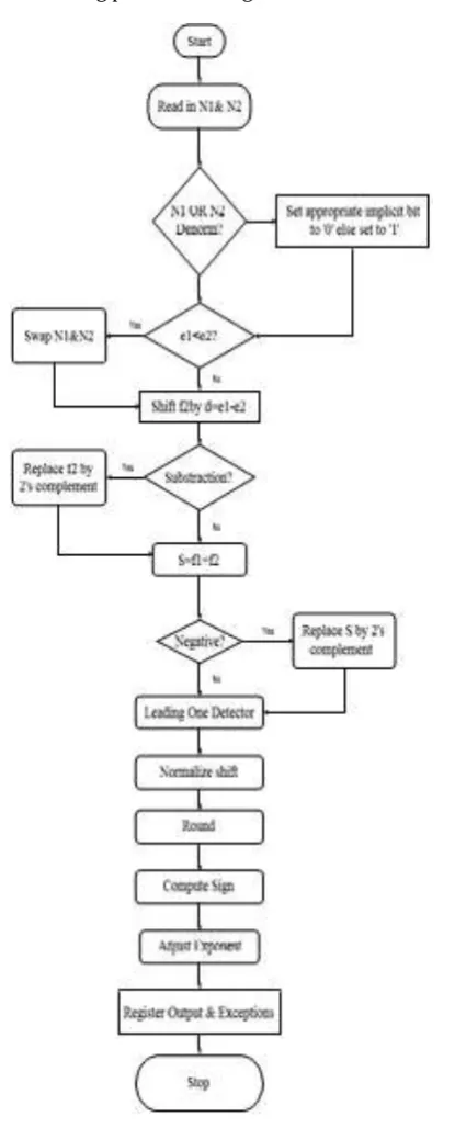
[image:2.595.60.268.228.743.2]Description of the Proposed Algorithm:
Fig 1 shows the flowchart of standard floating point adder algorithm. Let s1; e1; f1 and s2; e2; f2 be the signs, exponents, and significant of two input floating –point operands, N1 and N2, respectively. A description of the standard floating point adder algorithm is as follows.
Fig. 1: Flowchart of standard floating point adder Algorithm
1. The two operands, N1 and N2 are read in and
compared for demoralization and infinity. If numbers are demoralized, set the implicit bit to 0 otherwise it is set to 1. At this instant, the fraction part is extended to 24 bits.
2. The two exponents, e1 and e2 are compared
using 8-bit subtraction. If e1 is less than e2, N1 and N2 are swapped i.e. previous f2 will now be referred to as f1 and vice versa.
3. The minor fraction, f2 is shifted right by the
absolute difference result of the two exponents’ subtraction. Now both the numbers have the same exponent.
4. The 2 signs are used to see whether the
operation is a subtraction (-) or an addition (+).
5. If the process is a subtraction, the bits of the f2
are inverted.
6. At this instant the two fractions are added using
a 2’s complement adder.
7. If the outcome sum is a negative number, it has to
be inverted and a 1 has to be added to the result.
8. The outcome is then passed through a leading
one detector or leading zero counter. This is the first step in the normalization step.
9. Using the outcome from the leading one
detector, the result is then shifted left to be normalized. In some cases, 1-bit right shift is needed.
10. The outcome is then rounded towards nearest
even, the default rounding mode.
11. If the take out from the rounding adder is 1, the
result is left shifted by one.
12. Using the outcome from the leading one
© 2019, IRJET | Impact Factor value: 7.211 | ISO 9001:2008 Certified Journal
| Page 2460
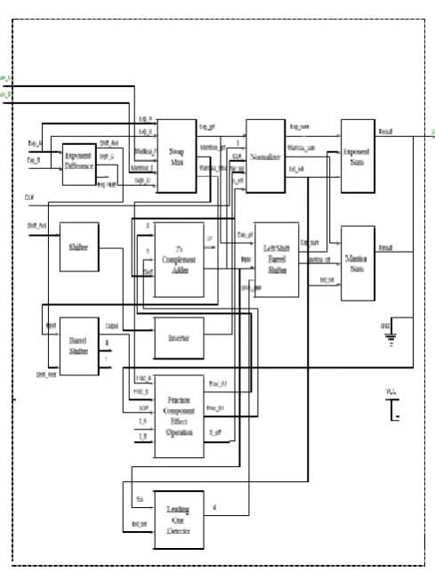
1.3 Block Diagram Of Single Precision Floating Point [image:3.595.38.283.116.438.2]Adder:-
Fig 2: Block Diagram of Single Precision floating-point Adder
Fig 2 shows the block diagram of single precision floating point adder. Num_A , Num_B ,CLK ,GND and VCC are inputs of the block diagram of single precision floating point adder. Output SUM is calculated by performing addition of Num_A and Num_B using floating point addition algorithm shown in Fig 1. It illustrate the main hardware modules necessary for floating point addition. The different modules are Exponent Difference Module, Swap Multiplexer, Shifter, Barrel Shifter , Fraction Component Effect Operation , 2’s Complement Adder , Inverter , Normalizer , Leading One Detector , Left Shift Barrel Shifter, Exponent Sum and Mantissa Sum.
Exp_a and Exp_b are the exponents of inputs Num_A and Num_B resp. Exp_a and Exp_b can be positive or negative numbers. The output shift_amt is given to the shifter and barrel shifter block for further calculation. Sign_d is given two the Swap Mux. Swap_Mux assigns greater Mantisa to Mantisa_grt and Lesser value of Mantisa to Mantisa_less and greater exponent is calculated and assigned to Exp_grt. Exp_grt output is given to the normalizer block, Mantisa_grt is given to the Fraction Component Effect Operation Block and Mantisa_less is given to the Barrel shifter Block respectively. The shifter is used to shift the significant of the smaller operand by the absolute exponent difference. Shifter is used to shift the data bits. The Output Shift_amt of Exponent
Difference Block is given as input to the Shifter block which gives output shifted_amt is further given to the inverter block. The inverter is used to invert the data bits of shifted amount. The normalizer block gives us normalized result. Later than the addition, the next step is to normalize the result. The primary step is to identify the leading or first one in the result. This outcome is used to shift left the adder result by the number of zeros in front of the leading one. In order to perform this operation, particular hardware, called Leading One Detector (LOD) or Leading Zero Counter (LZC), has to be implemented. Exponent sum and mantissa sum blocks are used to calculate the exponent and mantissa of output SUM and sign bit SOP is initially considered as 1.
1.4 Floating point Multiplication:-
The figure 3 shows the flowchart of multiplication algorithm of multiplication is demonstrated by flowchart. In1 and in2 are two numbers sign1, expo1, S1 and sign2, expo2, S2 are sign bit, exponent and significant of in1 and in respectively.
Steps for multiplication are as follows.
1:- calculate sign bit. sign_f= sign1 XOR sign2, sign_f is sign of final result.
2:- add the exponents and subtract 127 to make adjustment in exponent (expo1+127+expo2+127)-127.
3:- Multiply the significant. S=S1*S2.
4:- check for overflow and underflow and special flag. When the value of biased exponent is less than 1 it shows occurrence of underflow, if exponent is greater than 254 then it shows overflow of floating point operation.
5:- Take the first 23 bits of ‘S’ and from left side and discard remaining bits.
6:- Arrange the results in 32 bit format. 1 sign bit followed by eight bits exponent followed by 23 bits
Mantissa/significand.
Calculation of sign bit:- when both number have same sign the sign of result is positive else sign will be negative the sign in calculated by XORing both sign bits of inputs.
© 2019, IRJET | Impact Factor value: 7.211 | ISO 9001:2008 Certified Journal
| Page 2461
numbers). When underflow occur it makes underflow flag [image:4.595.40.283.134.546.2]high and the result goes to ±0 (+ or – signed is determined by the sign of two input numbers).
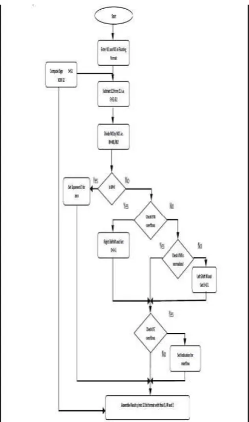
FIG 3:-Flowchart of standard floating point multiplication 1.5 Floating point division:-
The figure 4 shows the flowchart of division, algorithm for division is explained through this flowchart. In1 and in2 are two numbers sign1, expo1, S1 and sign2, expo2, S2 are sign bit, exponent and significant of in1 and in2 respectively. It is assumed that in1 andin2 are in normalized form.
Steps for floating point division are as follows.
1:- calculate sign bit. sign_f= sign1 XOR sign2, sign_f is sign of final result.
2:- divide the significand S1 by S2 for division binary division method is used.
• Expand divisor and dividend to double of their size
- Expanded divisor = divisor (24 bits MSB) zeroes (24 bits LSB)
- Expanded dividend = zeroes (24 bits MSB) dividend (32 bits, LSB)
• For each step, determine if divisor is smaller than dividend - Subtract divisor from dividend look at sign
- If result is greater than or equal to ‘0’: dividend/divisor>=1, mark quotient as “1”.
- If result is negative: divisor larger than dividend; make in quotient as “0”
• Shift quotient left and divisor right to cover next power of two.
3:- Subtract the expo2 from expo1.
[image:4.595.322.553.361.661.2]4:- check for overflow and underflow flags. 5: assemble the result in 32 bits format
© 2019, IRJET | Impact Factor value: 7.211 | ISO 9001:2008 Certified Journal
| Page 2462
2. EXPERIMENTAL RESULTS:-Simulation result of addition of two 32 bit floating point number. The round mode is 00 and the operation mode is 000
© 2019, IRJET | Impact Factor value: 7.211 | ISO 9001:2008 Certified Journal
| Page 2463
Simulation result of multiplication of two 32 bit floatingpoint number. The round mode is 01 and the operation mode is 010
Simulation result of division of two 32 bit floating point number. The round mode is 00 and the operation mode is 011
3. Conclusion and Future Work:-
This FPU has action as addition, subtraction multiplication, and division. Addition, subtraction and division have been implemented by conventional technique. The design of FPU has done using VHDL on Xilinx VIVADO 2014.4 and has implemented on Virtex-7 xc7v585tffg1157-3.We have proved that this FPU have requisite less memory but still we have a huge amount of work that can be set on this FPU to further make up the efficiency of the FPU by using other Vedic sutra. A single precision floating-point adder is implemented in this paper. The main contribution of our work is to implement and analyze floating-point addition algorithms and hardware modules were implemented using VHDL and is Synthesized using Xilinx ISE14.2 Suite. The results are obtained using ISim (VHDL/Verilog) Simulator. In order to expand our paper further some of the works can be proposed in order to accommodate any exponent and mantissa length. This will gives more versatility while
choosing the design criteria. The design can also be pipelined further for different number of pipeline stages to give even more adaptability and flexibility.
4. References:-
1) Ronald Vincent, Ms.Anju.S.L “Decimal Floating Point Format Based on Commonly Used Precision For Embedded System Applications.” International Conference on Microelectronics, Communication and Renewable Energy (ICMiCR-2013).
2) Somsubhra Ghosh, Prarthana Bhattacharyya and Arka Dutta “FPGA Based Implementation of a Double Precision IEEE Floating-Point Adder”, Proceedings of7'h International Conference on Intelligent Systems and Control (ISCO 2013).
3) Maarten Boersma, Michael Kr¨oner, Christophe Layer, Petra Leber, Silvia M. M¨uller, Kerstin Schelm “The POWER7 Binary Floating- Point Unit”, 2011 20th IEEE Symposium on Computer Arithmetic. 4) Reshma Cherian, Nisha Thomas, Y. Shyju
“Implementation of Binary to Floating Point Converter using HDL”P-461-P464.