C-Cube Mlcrosystems
r
CL450 MPEG Video Decoder
User's Manual
ii C-Cube Microsystems
C-Cube Microsystems reserves the right to change any products described herein at any time and without notice. C-Cube Microsystems assumes no responsibility or liability arising from the use of the prod-ucts described herein, except as expressly agreed to in writing by C-Cube Microsystems. The use and purchase of this product does not convey a licence under any patent rights, copyrights, trademark rights, or any other intellectual property rights of C-Cube Microsystems.
Trademark Acknowledgment:
C-Cube and CL450 are trademarks of C-Cube Microsystems.
The corporate logo is a registered trademark of C-Cube Microsystems. Motorola is a registered trademark of Motorola, Inc.
Intel is a registered trademark of Intel Corporation. © C-Cube Microsystems 1994
An rights reserved
C-Cube Microsystems 1778 McCarthy Boulevard
Milpitas, CA 95035 Telephone (408) 944-6300
Fax (408) 944-6314
Customer Comments and Feedback:
If you have any comments about this document, send them to the C-Cube Technical Publications Department at the address listed above, or send e-mail to:
Preface
This manual is the primary source of technical information for the op-eration and programming of the C-Cube CL450 MPEG Video Decoder.
This manual is intended for:
D System designers and managers who are evaluating the CL450 for
possible use in a system.
D Design, software and system engineers developing a video
decod-ing system usdecod-ing the CL450 for whom a comprehensive program-ming background as well as a detailed understanding of MPEG compression is assumed.
In particular, readers should understand the MPEG standard: Coded Representation of Picture, Audio and Multimedia/Hypermedia Informa-tion, ISO/IEC JTC lISC 29, December 6,1991.
As an aid to developing systems and applications based on the CL450, readers may also wish to obtain C-Cube's CL450 MPEG Video Decoder Sample Kit, which includes a sample development board, microcode and user's guide.
This manual is divided into three main sections:
D Section I, General Information, including an introduction to the
CL450 and the MPEG standard that it implements.
D Section II, Hardware Interface, including signal descriptions,
op-erational information for the main interfaces of the CL450, regis-ters, and detailed electrical and mechanical specifications.
Audience
Related
Publications
Organization
Conventions
iv C-Cube Microsystems
D Section III, Software Interface, including an overview of the
fun-damental mechanisms used to communicate between the host sys-tem and the CL450's microapplication, and an alphabetical listing of all macro commands and interrupts available to the program-mer. Note: the microapplication information in this manual ap-plies to CL450 versions 2.00 through 2.FF only.
Please note the following notation examples and conventions used in this manual: Notation Examples Ox1c3 110112 IMEM HOST_control CMEM_control
VIE Res
HMEM[3] CPU_control[O] HMEM[0][15] HMEM[3][2:0]
RESERVED or Res
leftBorder
return ( );
Explanation
"Ox" prefix indicates a hexadecimal number. "2"subscript indicates a binary number.
Four-letter mnemonics indicate on-chip memories, starting with a letter to indi-cate function of memory, and ending with "MEM."l For example, IMEM is the CL450's instruction memory.
This format indicates a register name. The first part of a register name is a group specifier, given in all upper-case. The second part (separated from the first by an underscore and given in all lower-case) is a register specifier, indi-cating the function performed by the register within the group. In the examples shown, HOST_control and CMEM_control are separate registers, even though both have the same register specifier, "control."
Italicized acronyms or abbreviations (initial or all caps) indicate bit field names within registers or data words.
Square bracket notation similar to C language array subscripting indicates words within memories, and bits within words and registers. HMEM[3], for ex-ample, is the 16-bit word at address 3 within HMEM, whi Ie CPU_control[O] is bit 0 of the CPU_control register. Similarly, HMEM[O][15] is the most significant bit of the word at HMEM address O.
Ranges of bits are indicated by numbers separated by a colon such as the three bits HMEM[3][2:0]. Ranges of words within a memory are indicated by numbers separated by a dash such as the eight words HMEM[0-7].
Indicates bit fields within registers which are not defined. RESERVED bit fields may return any value when read and must be written with 0 (or 1 if so speci-fied). Writing the incorrect value to a RESERVED CL450 register bit will cause indeterminate behavior. In addition, all CL450 registers which are not explicitly given names are also RESERVED, and accessing these registers may cause in-determinate results on current or future CL450 implementations.
Bold-face type represents macro command arguments.
C-style syntax presented in courier typeface represents program pseudocode and equations.
Names presented in courier represent names of items within the MPEG bit-stream taken from the MPEG standard.
Section I. General Information
1 Introduction
1.1 General Description 1.2 The CL450 Product Family
1.2.1 CL450 Features
1.2.2 Microapplication Features 1.3 Functional Description
1.4 Data Organization 1.4.1 CL450 Registers 1.4.2 CL450 Memories 1.5 Address Size
1.6 f>rogramming Overview 1.7 Typical Applications
2 MPEG Overview
2.1 MPEG Decoding
2.1.1 MPEG Stream Structure 2.1.2 General Decoding Process 2.1.3 Video Stream Data Hierarchy
Contents
1-1 1-1 1-2 1-3 1-4 1-5 1-5 1-6 1-6 1-7 1-8
2-2 2-2 2-2 2-3
2.2 Inter-picture Coding 2-6
2.2.1 Picture Types 2-6
2.2.2 Video Stream Composition 2-7
2.2.3 Motion Compensation 2-8
2.3 Intra-picture (Transform) Coding 2-10
2.4 Synchronization 2-11
2.4.1 System Clock References 2-11
2.4.2 Presentation Time Stamps 2-12
Section II. Hardware Interface
3 Signal Descriptions
3.1 Host Interface 3-2
3.1.1 Data Transfer Signals 3-3
3.1.2 DMA Signals 3-5
3.1.3 Interrupt Signals 3-6
3.1.4 Timing, Control, and Status Signals 3-7
3.2 DRAM Interface 3-10
3.3 Video Interface 3-11
3.4 Miscellaneous 3-13
4 Host Interface
4.1 Memory Access 4-2"
4.1.1 Register Access 4-4
4.1.2 local DRAM Access 4-4
4.1.3 CMEM Access 4-6
4.1.4 DMA Operation 4-6
4.1.5 Interrupt Vector Operation 4-6
4.2 local DRAM or Register Read 4-8
4.3 local DRAM or Register Write 4-9
4.4 CMEM Write Timing 4-11
4.5 CMEM DMA Write Timing 4-14
4.6 CMEM DMA Write Application Guidelines 4-16
4.7 CMEM level 4-18
4.8 Interrupt Cycle Timing 4-19
4.8.1 Polled Interupts 4-19
4.8.2 Vectored Interrupts 4-19
5 Local DRAM Interface
5.1 General Description 5-2
5.1.1 Amount of DRAM 5-2
5.1.2 Type and Organization of DRAM 5.2 Memory Bus Interface
5.2.1 Memory Interface Connections 5.2.2 Memory Design Guidelines 5.3 Memory Bus Timing
5.3.1 DRAM Page-Mode Read Timing 5.3.2 DRAM Page-Mode Write Timing 5.3.3 DRAM Refresh Timing
6 Video Display Interface
6.1 Digital Video Standards 6.2 Video Display Unit 6.3 Video Synchronization 6.4 Video Output
6.5 Video Output Enable Signal
7 Electrical and Physical Specifications
7.1 Operating Conditions 7.2 AC Timing Characteristics
7.2.1 Host Bus Memory and Register Timing 7.2.2 Host Bus CMEM Timing
7.2.3 Host Bus Vectored Interrupt Cycle Timing 7.2.4 Local DRAM Bus Timing
7.2.5 GCLK, SCLK, and
REm
Timing 7.2.6 Video Bus Timing7.3 Package Specifications 7.3.7 Pin List
7.3.8 Package Drawings
8 Registers
8.1 CL450 Register Categories 8.1.1 Direct-access Registers
8.1.2 Indirect-access (Video) Registers 8.2 CL450 Register Summary
8.3 Host Interface Registers 8.3.1 CMEM Registers
8.3.2 Interrupt Control Registers 8.3.3 Command/Status Registers 8.3.4 System Clock Reference Registers 8.4 Internal CPU Registers
8.4.1 CPU Execution Registers 8.4.2 IMEM Access Registers 8.4.3 TMEM Access Registers
8.5 DRAM Interface Register 8.6 Video Interface Registers
8.6.1 Direct-access Video Registers 8.6.2 Indirect-access Video Registers
Section III. Software Interface
9 Microapplication Overview
9.1 Process Configurations 9.1.1 Command Process
9.1.2 Bitstream Transfer Process 9.1.3 Decode Process
9.1.4 Display Process 9.2 Synchronization 9.3 Interrupts
10 Initialization
10.1 Registers
10.1.1 Default Settings 10.1.2 Loading Sequence 10.2 Microapplication
10.2.1 Default Settings 10.2.2 Loading Sequence 10.2.3 Halting
11 Macro Commands
11.1 Writing Macro Commands 11.2 Command States
11.2.1 ID LE State 11.2.2 PLAY-SETUP State 11.3 Command FIFO
11.4 Command Latency 11.5 Macro Command Groups
11.5.1 Set-type Commands 11.5.2 Play-type Commands 11.5.3 Control Commands 11.6 Macro Command Reference
AccessSCRO DisplayStillO FlushBitstreamO InquireBufferFullnessO
viii C-Cube Microsystems
NewPacket() 11-20
11.6.1 length Argument 11-22
11.6.2 timeStamp Arguments 11-22
11.6.3 Loading and Removing NewPacket Commands 11-23
Pause() 11-25
Play() 11-26
Reset() 11-27
Scan() 11-28
SetBlank() 11-29
SetBorder() 11-30
SetColorMode() 11-34
SetlnterruptMask() 11-36
SetThreshold() 11-38
SetVideoFormat() 11-40
SetWindow() 11-42
SingleStep() 11-45
SlowMotion() 11-46
12 Interrupts
12.1 Interrupt Types 12-2
12.1.1 Display-time Interrupt 12-3
12.1.2 Decode-time Interrupts 12-6
12.1.3 VSYNC Interrupts 12-6
12.2 Interrupt Handshaking 12-7
12.2.1 Microapplication Behavior 12-8
12.2.2 Host Behavior 12-11
12.3 Interrupt Listing 12-14
END-D 12-15
END-V 12-16
ERR 12-17
GOP 12-19
PIC-D 12-20
PIC-V 12-21
ROY 12-22
SeN 12-24
SEQ-D 12-25
SEQ-V 12-26
UNO 12-27
12.4 I nterrupt Examples 12-28
12.4.1 Interrupt Example 1: ROY, UNO, ERR 12-29
12.4.2 Interrupt Example 2: PIC-V, SCN 12-34
12.5 Servicing Interrupts 12-37
xC-Cube Microsystems
13 AudioNideo Synchronization
13.1 MPEG Conditions and Constraints 13-1 13.2 CL450 Synchronization Mechanism 13-2
13.2.1 CL450 SCR Counter 13-2
13.2.2 CL450 Presentation Time Stamps 13-2
13.2.3 CL450 Synchronization 13-3
13.3 Updating the CL450 SCR Counter 13-4
13.3.1 SCR Source and Drift 13-4
13.3.2 Automatic SCR Modifications 13-5 13.4 Using SCR Masters for Synchronization 13-5 13.4.1 Synchronizing to the Bitstream 13-5 13.4.2 Synchronizing to the Audio Decoder 13-6 13.4.3 Synchronizing from the CL450's SCR 13-6 13.4.4 Synchronizing from the CL450 and VSYNC 13-7 13.5 Transferring Coded Data to the CL450 13-7
13.5.1 Unpacketed Data Transfer 13-8
13.5.2 Packeted Data Transfer 13-8
13.5.3 Unpacketed/Packeted Data Transfer without PTSs 13-10 13.5.4 Packeted Data Transfer with one PTS 13-10 13.5.5 Packeted Data with Periodic PTSs 13-11
14 Host Access of DRAM Variables
14.1 Types of Variables
14.1.1 Sequence Variable Group 14.1.2 Picture Variable Group
14.2 Access Synchronization Using Semaphores 14.2.1 Reading DRAM-Resident Variables 14.2.2 Writing DRAM-Resident Variables 14.3 Timing Restrictions
15 CL450 Host-independent Operations
15.1 Frame Rate Conversion
15.2 Error Recovery and Concealment 15.2.1 During Picture Decode 15.2.2 During Header Decode 15.2.3 During Bitstream Underflow 15.3 Operating Restrictions
15.3.1 Bitstream
15.3.2 Output Window and Timing
Appendix A CL450 DRAM-Variable Allocation
Appendix B Microapplication Executable File Format
B.l Syntax Conventions B-1
B.2 File Structure B-2
B.3 File Header Structure B-2
B.4 Code Segment Structure B-5
Appendix C CL450 Microapplication Distribution Disk
Appendix D CL450 Troubleshooting
Index
1-1 Block Diagram ofthe CL450 1-2 Typical CL450 System Application 2-1 General MPEG Decoding System 2-2 MPEG Data Hierarchy
2-3 Location of Luminance and Chrominance Values 2-4 Macroblock Composition
2-5 Forward Prediction 2-6 Bidirectional Prediction
2-7 Typical Display Order of Picture Types 2-8 Video Stream versus Display Ordering 2-9 Transform Coding Operations
2-10 SCR Flow in MPEG System 3-1 Bus Connection Diagram 3-2 Data Transfer Signals 3-3 DMA Signals
3-4 Interrupt Signals
3-5 Timing, Control, and Status Signals 3-6 System Timer Block Diagram 3-7 DRAM Interface Signals 3-8 Video Interface Signals
3-9 Pixel Bus Definition, RGB Format
Figures
1-4 1-8 2-3 2-3 2-4 2-5 2-6 2-7 2-8 2-8 2-11 2-12 3-2 3-3 3-5 3-6 3-7 3-9 3-10 3-12 3-12
3-10 Pixel Bus Definition, YCbCr Format 3-13
4-1 Host Interface Block Diagram 4-2
4-2 Host Interface Diagram (detailed) 4-5
4-3 CMEM Block Diagram 4-7
4-4 Local DRAM or Register Read Timing 4-8 4-5 Local DRAM or Register Write Timing with Delayed
UlJS
andIDS
Timing Shown 4-9
4-6 DTACK State Logic Diagram 4-11
4-7 CMEM Write Timing 4-13
4-8 CMEM DMA Write Timing 4-15
4-9 Vectored Interrupt Cycle (with auto interrupt clearing) 4-21
5-1 DRAM Address Bus Configuration 5-4
5-2 Local DRAM Implementation with 256K x 16 DRAMs 5-5 5-3 Local DRAM Implementation with 256K x 4 DRAMs 5-6
5-4 Page-Mode Read Timing 5-8
5-5 Pag e-Mode Write Timing 5-10
5-6 "CAS-before-RAS Refresh Cycle 5-11
6-1 Typical Video Bus Connections 6-4
6-2 Example Video Frame 6-5
6-3 Vertical Timing 6-6
6-4 Horizontal Timing 6-7
6-5 VSYNC Timing Restriction 6-8
6-6 YCbCr Display Mode 6-9
6-7 RGB Display Mode 6-9
6-8 Video Output Enable Signal 6-10
6-9 Multiplexing Video Outputs Using \TOt 6-10 7-1 Timing Diagram - Host Bus Local DRAM Read 7-4 7-2 Timing Diagram - Host Bus Register Read 7-5 7-3 Timing Diagram - Host Bus Local DRAM Write 7-6
7-4 Host Bus Register Write 7-7
7-5 Timing Diagram - CMEM Write 7-9
7-6 Timing Diagram - CMEM DMA Write 7-10 7-7 Timing Diagram - Vectored Interrupt Cycle with Auto Clear 7-12 7-8 Timing Diagram - Local DRAM Bus Timing 7-14 7-9 Timing Diagram - Local DRAM "CAS-before-RAS" Refresh 7-15
7-10 GCLK Timing Diagram 7-17
7-11
"REm
Timing Diagram 7-177-12 Timing Diagram - SCLK Input 7-18
7-13 Timing Diagram - Video Bus Inputs 7-18
7-14 VCLK Timing (20 MHz only) 7-19
7-15 CL450 PQFP Pinout Diagram 7-21
7-16 Plastic Quad Flat Pack Physical Dimensions 7-25
8-1 Internal Register Structure of the CL450 8-6 8-2 Internal Structure of the Host Interface Module 8-7 8-3 Motorola and Intel Byte Ordering 8-8
8-4 Command Write Data Flow 8-15
8-5 Internal CPU Registers 8-18
8-6 IMEM Write Data Flow 8-20
8-7 DRAM Interface Register 8-22
8-8 Video Interface Registers 8-24
8-9 Binary Representations of Conversion Coefficients 8-27 9-1 CL450 Microapplication Process Configurations 9-2 9-2 CL450 Decoding Process Configuration 9-3 9-3 Programmed Transfer of Coded Data to the CL450 9-6
9-4 Mask Bit Allocation 9-8
11-1 Issuing a Macro Command to the CL450 11-3 11-2 Command State Transition Diagram 11-5
11-3 CL450 Command FIFO Example 11-8
11-4 AccessSCRO Arguments Block Diagram 11-13
11-5 Still Picture Bitstream Format 11-15
11-6 CL450's State with Regard to Host NewPacketO Commands 11-21 11-7 Packet Representation in Command FIFO vs. Bitstream Buffer 11-24
11-8 Video Display Configuration 11-31
11-9 Video Display Configuration - SetWindow() 11-43 12-1 VSYNC Field Period Display for NTSC vs. PAL Environments 12-3 12-2 Display-time I nterrupt Generation 12-4
12-3 VSYNC Interrupt Generation 12-7
12-4 CL450 Interrupt Posting Procedure (pseudocode 12-9 12-5 CL450 Interrupt Posting Procedure (block diagram) 12-10 12-6 Host Interrupt Handler Example 1 12-12 12-7 Host Interrupt Handler Example 2 12-14
12-8 Key to Interrupt Examples 12-29
12-9 Interrupt Example 1: RDY, UND, ERR 12-30 12-10lnterrupt Example 2: PIC-V, SCN 12-35 13-1 Association of NewPacket() Commands and Bitstream 13-3 13-2 Bitstream/NewPacket() Association 13-9 14-1 DRAM-Resident Sequence Variable Group Variables 14-3 14-2 INTRA_Q and NON_INTRA_Q Matrix Ordering 14-3 14-3 DRAM-Resident Picture Variable Group Variables 14-4 14-4 Allocate Semaphore Function Pseudocode 14-6
14-5 DRAM Variable Read Pseudocode 14-7
14-6 DRAM Variable Write Pseudocode 14-8
15-1 B-picture Decode and Display 15-7
Tables
1-1 Address Size of CL450 Memories 1-7
3-1 Meaning of UDS and IDS" 3-4
3-2 Internal Module Selected by A[20:19] 3-4
4-1 CL450 Memory Access Address Bits 4-3
4-2 LOS and UDS Decoded Values 4-3
4-3 CMEM Level Control Bits 4-18
7-1 Absolute Maximum Ratings 7-2
7-2 Operating Conditions 7-2
7-3 DC Characteristics 7-2
7-4 Timing Characteristics - Local DRAM or Register Access 7-8 7-5 Timing Characteristics - CMEM Access 7-11 7-6 Timing Characteristics - Vectored Interrupt Cycle with
Auto Clear 7-13
7-7 Timing Characteristics - Local DRAM Bus 7-16 7-8 Timing Characteristics - GCLK and RESET 7-17 7-9 Timing Characteristics - SCLK Input 7-18 7-10 Timing Characteristics - Video Bus Inputs 7-19
7-11 Host Bus Interface Pins 7-22
7-12 DRAM Bus Interface Pins 7-23
7-13 Video Bus Interface Pins 7-24
7-14 Power and Miscellaneous Pins 7-24
7-15 Plastic Quad Flat Pack Physical Dimensions 7-26 8-1 Direct-access Registers (listed by category) 8-3 8-2 Indirect-access (Video) Registers (listed by category) 8-4 8-3 Direct-access Registers (described) 8-5 8-4 Indirect-access (Video) Registers (described) 8-5
8-5 CMEM Empty Status Bits 8-10
8-6 CFLEVEL Assertion Control 8-10
8-7 Interrupt Mode Values 8-12
8-8 Video Register IDs 8-25
9-1 Macro Command Summary 9-4
9-2 CL450 Interrupt Summary 9-9
10-1 Automatic Register Defaults 10-3
10-2 Macro Commands for Loading Registers 10-5
10-3 Macro Command Defaults JO-6
10-4 MPEG Decoding Defaults, Sequence Layer 10-7 10-5 MPEG Decoding Defaults, GOP Layer 10-7
10-6 Host/CL450 Interface Defaults 10-8
10-7 DRAM-Resident Variable Defaults 10-8
11-1 HMEM Address Allocation 11-2
11-2 Macro Command Summary 11-11
11-3 Filter Argument Encoding 11-18
11-4 SetBorderO Argument Restrictions: leftBorder and topBorder 11-32
11-5 Video Border Sizes 11-32
11-6 Mask Bit Assignments 11-36
11-7 Video Format Summary 11-40
11-8 SetWindowO Argument Restrictions 11-44 11-9 Picture Decode Play Rate while in SLOW State 11-47
12-1 CL450 Interrupt Summary 12-2
14-1 PIC_SEM / SEQ_SEM DRAM Location Encoding 14-5
14-2 Maximum DTACK Pulse Width 14-9
15-1 Picture Display Rates: Play Speed vs. Nominal Speed 15-2 A-1 DRAM Addresses for Host Scratch Storage A-1 A-2 DRAM Addresses for Sequence Variable Group A-2
A-3 DRAM Addresses for INTRA_Q Matrix A-3
A-4 DRAM Addresses for NONJNTRA_Q Matrix A-3 A-5 DRAM Addresses for Picture Variable Group A-3 A-6 DRAM Addresses for Microapplication Version Information A-4
B-1 Executable File Syntax Symbols B-2
Chapter
1
Introduction
The C-Cube CL450 ™ is the world's first single-chip MPEG video de-coder. It is designed to provide full-motion video capability for cost-sensitive consumer electronics products. The CL450 decompresses constrained-parameters MPEG bitstreams (typically SIF resolution) in real time. SIF resolution is 352 x 240 pixels at 30 Hz or 352 x 288 pixels at 25 Hz, with typical compressed data rates of 1.2 to 3 Mbits per sec-ond.
The CL450 interpolates decompressed pictures horizontally (typically to 704 pixels per scan line) before outputting them. The CL450 outputs decompressed pictures multiple times to increase the frame rate from 24,25, or 30 Hz (coded frame rate) to 50 or 60 Hz (display frame rate). The CL450 can change the display position of decompressed pictures relative to its HSYNC and VSYNC inputs.
The CL450 isa fully-integrated MPEG decoding engine whose func-tionality is an intertwined combination of hardware and microapplica-tion set provided by C-Cube, as explained in the software interface section of this manual, Section III.
1.1
General
Description
1.2
The CL450 Product Family
1.2.1 CL450 Features
The basic CL450 product includes these features:
o Fully complies with all requirements of the MPEG standard (ISO CD 11172)
o Performs real-time decoding of SIF-resolution bitstreams (352 x 240 pixels at 30 Hz or 352 x 288 pixels at 25 Hz)
o Performs real-time horizontal pixel interpolation and frame dupli-cation to produce output formats of 704 x 240 pixels at 60 Hz or 704 x 288 pixels at 50 Hz
o Provides either RGB or YCbCr video output using an on-chip col-or-space converter
o Supports NTSC and PAL video output timing formats
o Interfaces to 680xO processors and DRAM with no external logic
o Requires only 4 Mbits of 80-ns DRAM to decode SIF-resolution MPEG bitstreams
o Provides hardware and microapplication support for audio/video synchronization
o Decodes Huffman variable-length codes at a peak rate of 4 bits per clock (160 Mbits/second at 40 MHz)
o Allows the active display window to be positioned relative to HSYNC and VSYNC inputs with one-pixel and one-HSYNC ac-curacy, respectively
o Displays all or part of decompressed pictures; displayed section can be selected to one-pixel accuracy (within the decoded picture) and can be changed every coded frame for panning motion video o Supports host access of local DRAM including byte writes
o Supports both programmed I/O and DMA transfers of compressed bitstreams from the host
o Is fabricated in a CMOS process
o Is supplied in a 160-pin plastic quad flat-pack (PQFP)
1.2.2 Microapplication Features
The CL450 microapplication includes these features:
o 18 macro commands, allowing the host to control interactive play-back, CL450 configuration, and audio/video synchronization:
o AccessSCRO
o DisplayStillO o FlushBitstreamO
o InquireBufferFullnessO
o NewPacketO
o PauseO
o PlayO
o ResetO
o ScanO
o SetBlankO
o SetBorderO
o SetColorModeO
o SetlnterruptMaskO
o SetThresholdO
o SetVideoFormatO
o SetWindowO
o SingleStepO
o SlowMotionO
o 11 interrupts, providing the host feedback on bitstream transition, display, and decoding processes
o Bit rate up to 5.0 Mbits per second
o Transcoding between NTSC and PAL input and output frame rates
o System memory expansion capability
o Support for 24-Hz film format input
o Display window positioning within decoded picture to single-pix-el accuracy
o Flagged and unfIagged error concealment
o MPEG double vertical-resolution still pictures
The CL450 Product Family
Functional Description Host Data Addr Control
1.3
Functional Description Interface(6 ~
..
Host20
, Interface..
- (7 ~
[image:23.507.41.397.203.537.2]'Il ,f Coded Data FIFO CL450
Figure 1-1 shows a block diagram of the CL450, which has three inter-faces:
D The host interface: Connects directly to 680xO processors with no
external logic. It can also be easily connected to 80x86 processors.
D The DRAM interface: Reads from and writes to the local DRAM
with no external logic .
D The video interface: Outputs pixel data to a video monitor or other
video processing device.
Huffman Decoding Engine
t
Central ProcessingVideo I
Unit nterface
Video L-"o
24
DRAM Display
~ Controller
...
Unit.
-
/4 /Data
Control
~, 'Il
16// 10
v
7)/DRAM Interface Data Addr Control
,ir
"
"Bitstream Buffer
I
Frame BuffersW
Local DRAM 14 Mbits minimum)
Figure 1-1 Block Diagram of the CL450
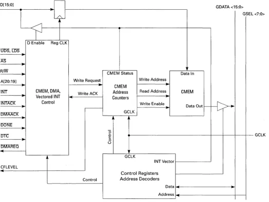
The host computer supplies compressed (coded) data to the CL450 via the host interface. The CL450 buffers up to 16 coded data words in an internal coded data FIFO, called CMEM, from which the data words are read by the DRAM controller and written into the bitstream buffer in the local 4-Mbit DRAM.
The on-chip central processing unit (CPU) interprets commands issued by the host processor, works with the Huffman decoding engine to per-form the decompression process, and writes decompressed pixel data into the frame buffer in the local DRAM.
The video display unit reads decompressed pixel data from the frame buffer, sends it through the color-space converter if necessary, and out-puts the pixel data on the video bus.
Data Organization
Though the CL450 can be used with many different processors, it has
1.4
been optimized for use with the Motorola 68070 processor.
Data Organization
1.4.1 CL450 Registers
Each of the 34 registers of the CL450 is 16 bits wide and is accessed by word operations which cover the entire 16-bit width. The least signifi-cant bit of each address is bit 0, and the most signifisignifi-cant bit is bit 15. Even though CL450 register addresses may be expressed as byte ad-dresses, the CL450 does not support single-byte access to its internal registers; instead, all CL450 register accesses must be made using 16-bit operations (i.e., 16 16-bits at a time) as shown below.
15 14 13 12 11 10 9 8 7 6 5 4 3 2
MSB Word 0
Word 1
Word 2
o
LSB
Address Size
1.4.2 CL450 Memories
All on-chip memory transactions on the CL450 must be 16 bits (as shown in the previous figure), while the local (off-chip) DRAM may be accessed by the host through the CL450 using single-byte access. When byte-addressable access to local DRAM is performed, the higher-order byte has an even address twice (2x) that of the word (shown be-low), and the low-order byte has an odd address that is one count higher than twice the word address (2x
+
1). The UDS (Upper Data Strobe) and the LDS (Lower Data Strobe) signals distinguish byte operations from word operations as explained in Chapter 4.15 14 13 12 11 10 9 8 7 6 5 4 3 2
o
1.5
Address Size
Byte 0 Word 0 Byte 1
I
Word 1 Byte 2
I
Byte 3·
·
·
Byte FFFFE Word 7FFFF Byte FFFFF
I
The size of CL450 addresses within a memory (on-chip memories or the off-chip DRAM) are given in units which are the same as the word size of the RAM in question. For example, the off-chip DRAM is configured as 256K or 512K words of 16 bits each, with DRAM addresses there-fore being within the range 0 to Ox3ffff or Ox7ffff words and each dis-tinct address containing a 16-bit value.
The word size of the CL450 memories are shown in Table 1-1.
Table 1-1 Address Size of CL45D Memories
Memory
On-chip registers Off-chip (local) DRAM
HMEM IMEM TMEM CMEM
Address Unit Size
16 bit 16 bit 16 bit 32 bit 24 bit 16 bits
Note: Writing host software to interact with the CL450 on byte-addressable processors may necessitate multiplying the given DRAM and register addresses by 2.
The CL450 performs its higher-level functions by executing a microap-plication. The microapplication must be loaded into the CL450 by a software driver before the CL450 is fully operational. C-Cube provides C-Ianguage source code for a loader, which users may modify and com-pile on their target system.
Application programs access the CL450 in two ways:
o Registers: Some of the CL450' s internal registers are accessed by application programs to set key operating parameters during ini-tialization and operation. Other CL450 registers are used to load command IDs and arguments for the macro commands described below and to determine the status of microapplication execution. Chapter 8, Registers, describes the use and format of the CL450' s registers.
o Macro commands: Use of these commands is the primary method for communicating between the host software and the microappli-cation executing on the CL450's CPU. Section 1.2.2 on page 1-3 shows the macro commands implemented in the CL450 microap-plication set. Section III of this manual, Software Interface, de-scribes the syntax and use of each macro command.
Programming Overview
1.6
Programming
Overview
Typical Applications
1.7
Typical
Applications
The CL450 MPEG decoder is designed for low-cost consumer applica-tions such as:
D CD-I systems D Video games
D Interactive multimedia systems D Point-of-sale/information kiosks D Interactive TV
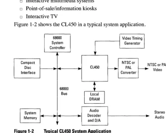
Figure 1-2 shows the CL450 in a typical system application.
68000
I
Video TimingI
System
1
I
GeneratorController
Compact NTSC or N
Disc
-
CL450r---.
PALr---.
Interface Converter
68000
~
Bus
I
Local
I
DRAM
I
System
..
Audio-
...
..
- --"'" Decoder Memory [image:27.508.35.466.80.571.2] [image:27.508.116.452.145.413.2]-and D/A
Figure 1-2 Typical Cl450 System Application
TSC or PAL Video
Stereo Audio
2
MPEG Overview
This chapter presents an overview of the Moving Picture Experts Group (MPEG) standard that is implemented by the CL450. The standard is of-ficially known as ISO/IEC Draft Standard Coded representation of
pic-ture, audio and multimedia/hypermedia information, CD 11172,
December 6, 1991.1t is more commonly referred to as the MPEG stan-dard.
MPEG Decoding
2.1
MPEG Decoding
This section explains the general structure of an MPEG stream and in-troduces some basic concepts used in the rest of the chapter.
2.1.1 MPEG Stream Structure
In its most general form, an MPEG stream is made up of two layers: o The system layer contains timing and other information needed to
demultiplex the elementary audio and video streams and to syn-chronize audio and video during playback.
o The compression layers include the elementary audio and video streams.
2.1.2 General Decoding Process
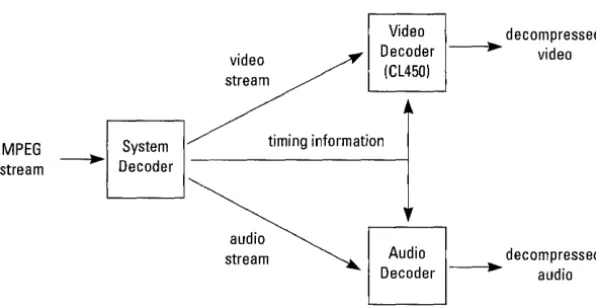
Figure 2-1 shows a generalized decoding system using the CL450 as the decoder for the elementary video stream.
The system decoder extracts the timing information from the MPEG system stream and sends it to the other system components. (Section 2.4, Synchronization, has more information about the use of timing in-formation for audio and video synchronization.) The system decoder also demultiplexes the elementary video and audio streams from the system stream and sends each to the appropriate decoder. In many ap-plications, the system decoder function is implemented as a software program on the host computer.
The video decoder decompresses the elementary video stream as spec-ified in Part 2 of the MPEG standard. (See Section 2.2, Inter-picture Coding, and Section 2.3, Intra-picture Coding, for more information about video compression.) The CL450 performs the video decoding function.
The audio decoder decompresses the audio stream as specified in Part 3 of the MPEG standard.
video stream
Video decompressed Decoder - . . video
(CL450)
MPEG System timing information stream ~ Decoder
audio
[image:30.510.60.358.76.230.2]stream Audio decompressed Decoder - . . audio
Figure 2-1 General MPEG Decoding System
2.1.3 Video Stream Data Hierarchy
The MPEG standard defines a hierarchy of data structures in the video stream as shown schematically in Figure 2-2.
Video Sequence
Group of Pictures
.1
MPEG Decoding
DDDDDDDD
Block
Slice Macroblock
-t
8
-
.. I
I lerJ=Q..
Figure 2-2 MPEG Data Hierarchy
[image:30.510.40.450.324.534.2]MPEG Decoding
Video Sequence
A sequence begins with a sequence header (and may contain additional sequence headers), includes one or more groups of pictures, and ends with an end-of-sequence code.
Group of Pictures (GOP)
A header followed by a series of one or more pictures; intended to allow random access into the sequence.
Picture
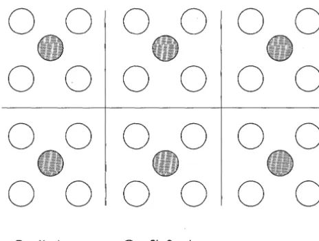
[image:31.510.142.374.360.535.2]The primary coding unit of a video sequence. A picture consists of three rectangular matrices representing luminance (Y) and two chrominance (Cb and Cr) values. The Y matrix has an even number of rows and col-umns. The Cb and Cr matrices are each one-half the size of the Y matrix in both directions, horizontal and vertical.
Figure 2-3 shows the relative x-y locations of the luminance and chrom-inance components. Note that for every four lumchrom-inance values, there are two associated chrominance values: one Cb value and one Cr value. (The location of the Cb and Cr values is the same, so only one circle is shown in the figure.)
0 0 0 0 0 0
0 0 0 0 0 0
0 0 0 0 0 0
0 0 0 0 0 0
o
= Yvalue = Cb, Cr valueFigure 2-3 Location of Luminance and Chrominance Values
Slice
One or more "contiguous" macroblocks. The order of the macroblocks within a slice is from left to right and top to bottom.
Slices are important in the handling of errors. If the bitstream contains an error, decoders may skip to the start of the next slice. Having more slices in the bitstream allows better error concealment but uses bits that could otherwise be used to improve picture quality.
Macroblock
A 16-pixel by 16-line section of luminance components and the corre-sponding 8-pixel by 8-line sections of the two chrominance compo-nents. See Figure 2-3 for the spatial location of luminance and chrominance components. A macroblock contains four Y blocks, one Cb block and one Cr block as shown in Figure 2-4. The numbers corre-spond to the ordering of the blocks in the data stream, with block 1 first.
y Cb Cr
Figure 2-4 Macroblock Composition
Block
A block is an 8-pixel by 8-line set of values of a luminance or a chrom-inance component. Note that a lumchrom-inance block corresponds to one-fourth as large a portion of the displayed image as does a chrominance block.
MPEG Decoding
Inter-picture Coding
2.2
Inter-picture
Coding
Much of the information in a picture within a video sequence is similar to information in a previous or subsequent picture. The MPEG standard takes advantage of this temporal redundancy by representing some pic-tures in terms of their differences from other (reference) picpic-tures, or what is known as inter-picture coding. This section describes the types of coded pictures and explains the techniques used in this process.
2.2.1 Picture Types
The MPEG standard specifically defines three types of pictures used for inter-coding: intra, predicted, and bidirectional.
Intra Pictures
Intra pictures, or I-pictures, are coded using only information present in the picture itself. I-pictures provide potential random access points into the compressed video data. I-pictures use only transform coding (as ex-plained in Section 2.3 on page 2-10) and provide moderate compres-sion. I-pictures typically use about two bits per coded pixel.
Predicted Pictures
Predicted pictures, or P-pictures, are coded with respect to the nearest previous 1- or P-picture. This technique is called forward prediction and is illustrated in Figure 2-5.
Like I-pictures, P-pictures serve as a prediction reference for B-pictures and future P-pictures. However, P-pictures use motion compensation (see Section 2.2.3) to provide more compression than is possible with 1-pictures. Also unlike I-pictures, P-pictures can propagate coding errors because P-pictures are predicted from previous reference (1- or P-) pic-tures.
Forward Prediction
Figure 2-5 Forward Prediction
Bidirectional Pictures
Bidirectional pictures, or B-pictures, are pictures that use both a past and future picture as a reference. This technique is called bidirectional prediction and is illustrated in Figure 2-6. B-pictures provide the most compression and do not propagate errors because they are never used as a reference. Bidirectional prediction also decreases the effect of noise by averaging two pictures.
Bidirectional Prediction
Figure 2-6 Bidirectional Prediction
2.2.2 Video Stream Composition
The MPEG standard allows the encoder to choose the frequency and lo-cation of I-pictures. This choice is based on the applilo-cation's need for random accessibility and the location of scene cuts in the video se-quence. In applications where random access is important, I-pictures are typically used two times a second.
The encoder also chooses the number of B-pictures between any pair of reference (1- or P-) pictures. This choice is based on factors such as the amount of memory in the encoder and the characteristics of the material being coded. For a large class of scenes, a workable arrangement is to have two bidirectional pictures separating successive reference pic-tures. A typical arrangement of 1-, P-, and B-pictures is shown in Figure 2-7 in the order in which they are displayed.
Inter-picture Coding
Inter-picture Coding
1 second
2 B-pictures between reference (P) pictures
I-picture every 15th frame (1/2 second at 30 Hz)
A
Picture Type: I B B P B B P B B P B B P B BIB B P B B P B B P B B P B B Display order: 1 2 3 4 5 6 7 8 9 10 1112 13 14 15 16 17 18 19 20 2122 23 24 25 26 27 28 29 30
Figure 2-7 Typical Display Order of Picture Types
The MPEG encoder reorders pictures in the video stream to present the pictures to the decoder in the most efficient sequence. In particular, the reference pictures needed to reconstruct B-pictures are sent before the associated B-pictures. Figure 2-8 demonstrates this ordering for the first section of the example shown above.
Display Order
2 3 4 5 6 7
Video Stream Order
4 2 3 7 5 6
Figure 2-8 Video Stream versus Display Ordering
2.2.3 Motion Compensation
Motion compensation is a technique for enhancing the compression of P- and B-pictures by eliminating temporal redundancy. Motion com-pensation typically improves compression by about a factor of three compared to intra-picture coding. Motion compensation is performed at the macroblock level.
When a macroblock is compressed by motion compensation, the com-pressed file contains this information:
o One or two spatial vectors between the reference macroblock area and the macroblock being coded (motion vectors)
o The content differences between the reference macroblock area and the macroblock being coded (error terms)
However, not all information in a picture can be predicted from a previ-ous picture.
Consider a scene in which a door opens: The visual details of the room behind the door cannot be predicted from a previous frame in which the door was closed. When a case such as this arises-i.e., a macroblock in a P-picture cannot be efficiently represented by motion compensation-the picture is coded in compensation-the same way as a macroblock in an I-picture us-ing transform codus-ing techniques (see Section 2.3, Intra-picture Codus-ing). The difference between B- and P-picture coding is that macroblocks in a P-picture are coded using the previous reference (1-or P-picture) only, while macroblocks in a B-picture are coded using any combination of a previous and/or future reference picture.
Four codings are therefore possible for each macroblock in a B-picture:
o Intra coding: no motion compensation
o Forward prediction: the previous reference picture is used as a ref-erence
o Backward prediction: the next reference picture is used as a refer-ence
o Bidirectional prediction: two reference pictures are used, the pre-vious reference picture and the next reference picture
Backward prediction can be used to predict uncovered areas that do not appear in previous pictures.
Inter-picture Coding
Intra-picture (Transform) Coding
2.3
Intra-picture
(Transform) Coding
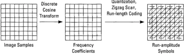
The MPEG transform, or intra-picture, coding algorithm includes these steps:
D Discrete cosine transform (DCT) D Quantization
D Run-length encoding
Both image blocks and prediction-error blocks have high spatial redun-dancy. To reduce this redundancy, the MPEG algorithm transforms 8 x 8 blocks of pixels or 8 x 8 blocks of error terms from the spatial domain to the frequency domain with the Discrete Cosine Transform (DCT). Next, the algorithm quantizes the frequency coefficients. Quantization is the process of approximating each frequency coefficient as one of a limited number of allowed values. The encoder chooses a quantization matrix that determines how each frequency coefficient in the 8 x 8 block is quantized. Human perception of quantization error is lower for high spatial frequencies, so high frequencies are typically quantized more coarsely (i.e., with fewer allowed values) than low frequencies. The combination of DCT and quantization results in many of the fre-quency coefficients being zero, especially the coefficients for high spa-tial frequencies. To take maximum advantage of this, the coefficients are organized in a zigzag order to produce long runs of zeros (see Figure 2-9). The coefficients are then converted to a series of run-amplitude pairs, each pair indicating a number of zero coefficients and the ampli-tude of a non-zero coefficient. These run-ampliampli-tude pairs are then coded with a variable-length code, which uses shorter codes for commonly oc-curring pairs and longer codes for less common pairs.
Some blocks of pixels need to be coded more accurately than others. For example, blocks with smooth intensity gradients need accurate coding to avoid visible block boundaries. To deal with this inequality between blocks, the MPEG algorithm allows the amount of quantization to be modified for each macroblock of pixels. This mechanism can also be used to provide smooth adaptation to a particular bit rate.
Figure 2-9
Frequency Coefficients
Transform Coding Operations
Run-amplitude Symbols
The MPEG standard provides a timing mechanism that allows for syn-chronization of audio and video. The standard includes two parameters in the systen layer of a bitstream which are used by the CL450: the sys-tem clock reference (SCR) and the presentation time stamp (PTS). The MPEG-specified "system clock" runs at 90 kHz and generates 7.8 x 10⁹ clock ticks in a 24-hour day. System clock reference and presen-tation time stamp values are coded in MPEG bitstreams using 33 bits, which can represent any clock period in a 24-hour period.
2.4.1 System Clock References
A system clock reference is a snapshot of the encoder system clock which is placed into the system layer of the bitstream, as shown in Fig-ure 2-10. During decoding, these values are used to update the clock counter(s) in the system decoder before being sent to the audio and vid-eo decoders. This is typically done in a system in which MPEG data is delivered at a fixed bit rate, and effectively locks the decoder's time base with that of the encoder and the bitstream transport mechanism. The CL450 contains an on-chip counter which it uses as its clock for performing synchronization. The host may update the CL450's clock with SCR information from the bitstream (in fixed bit-rate systems) or from some other accurate, decoder-wide time base.
Synchronization
2.4
Synchronization
Synchronization
Video
ICL450) MPEG stream
with SCRs /
Decoder
r - - - 1 ' - - - '
MPEG
Encoder
t
Encoder
System
Clock
System
---J.~ Decoder
Figure 2-10 SCR Flow in MPEG System
2.4.2 Presentation Time Stamps
SCRs
~
AudioDecoder
Presentation time stamps are samples of the encoder system clock that are associated with video or audio presentation units. A presentation unit is a decoded video picture or a decoded audio sequence. The PTS represents the time at which the video picture is to be displayed or the starting playback time for the audio time sequence.
Elementary video or audio decoders use the PTS values associated with each presentation unit to adjust their decoding rate so that each presen-tation unit is presented (displayed or played) at the correct time as mea-sured by the decoder's system clock.
3
Signal Descriptions
This chapter describes the signals that comprise the external physical interface to the CL450. The information presented for each signal in-cludes the signal mnemonic and name, type (input, output, or bidirec-tional), and description. For information about the functional operation of the CL450, including functional waveforms, see Chapters 4, 5, and 6. For timing information, see Chapter 7.
This chapter is divided into three sections that correspond to the com-ponents that interface to the CL450:
o 3.1: Host Interface o 3.2: DRAM Interface o 3.3: Video Interface
Host Interface Q) (,) <0 't: 2 c t) 0 I Data Transfer Signals (see Figure 3-2) DMA Signals
(see Figure 3-3)
Interrupt Signals
(see Figure 3-4)
Timing, Con-trol and Status Signals (see
Figure 3-5)
3.1
Host Interface
,. A[20:1] p UITS
IDS
,. AS
R/W
-
0[15:0].... ,.
OTACK
..
DMAREQ~
DMAACK
po
nrc
p lJOl\JE{
-
~ Tf\JT Tl\JTACK~ CFLEVEL
RESET
.
GCLK HCLK _..
SCLK p TEST CL450 PD[23:0] HSVf\J"C VSYNC V'OE VCLK MD[15:0] MA[9:0] RAS[1:0] UCAS LeAS OCASIN ITASTf\r WE ~ ...L ~ --~ ...L ~..
,. ,--"
.
Video Signals
(see Figure 3-8)
DRAM Signals
[image:41.509.58.443.78.397.2](see Figure 3-7)
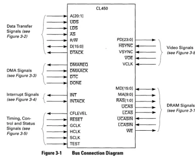
Figure 3-1 Bus Connection Diagram
The host interface signals divide logically into these functional groups:
o Data transfer signals: These signals comprise the address and data buses and the control signals used for data transfer handshaking.
o DMA signals: The CL450 uses these signals to implement the SCC68070 DMA protocol. This is a subset of that used by the 68000 family of DMA controllers.
o Interrupt signals: These signals provide a request-acknowledge handshake used by the CL450 to request vectored interrupt service from the host.
o Timing, control, and status signals: These signals include the-clocks and reset signals, and the CMEM status signal.
Note: The following description of host interface signals is based on the Motorola MC680XOfamily of microprocessors, even though the CL450 works with a wide range of other processors and corresponding address widths.
3.1.1 Data Transfer Signals
These signals are used to communicate between the CL450 and the host processor. Figure 3-2 shows how the data transfer signals of the CL450 connect to the host processor. The various modes of transferring data are discussed in Sections 4.2 through 4.5.
UlJS IDS
AS (Add. Strobel
/
*A[23:21] /
..
A[20:1] 0[15:0]
-R/W rrrACK ... Host Processor
*These bits pertain exclusively to the 680XO example: the left-over bits of a 24-bit address bus. Other bits may be chosen for other processors.
I
, ,
Comb. Logic** / / L /I I I
rrrACKfrom other devices
Figure 3-2 Data Transfer Signals
UDS - Upper Data Strobe LDS - Lower Data Strobe
..
UlJS ~ ---- IDS..
AS~
..
A[20:1] ~..
~ 0[15:0]..
~ R/W rrrACKCL450
**If the host processor is a 680XO, we recommend qualifying the AS input of the CL450 with UDS or IDS so that set-up time can be added on RfW.
Input Input
The host processor uses 'O'I)S" and r:::DS" to indicate the byte va-lidity and transfer size of D[15:0] as shown in Table 3-1. The CL450's local DRAM (accessed when A[20] is 0) is the only CL450 resource which supports byte-wide accesses; at all other times Ui5S must equal LDS.
Host Interface
Host Interface
Table 3-1
Table 3-2
3-4 C-Cube Microsystems
Meaning of
DDS
and LDSODS IDS Valid Size
High High 0[15:0] not valid none Low High 0[15:8] (DRAM only) byte High Low 0[7:0] (DRAM only) byte Low Low 0[15:0] word
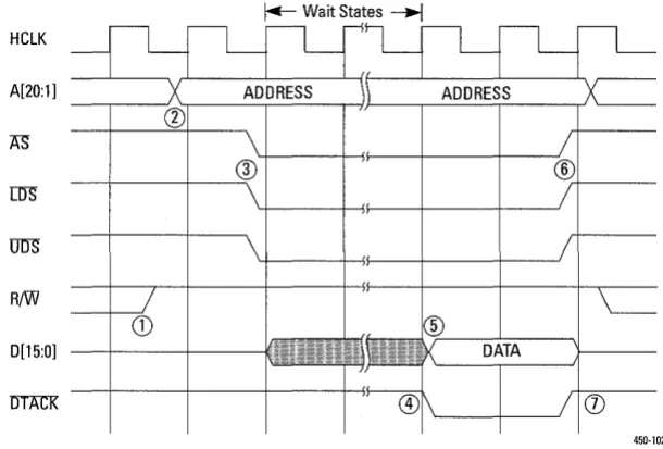
AS - Address Strobe Input
The host processor asserts A"S (active low) to select the CL450 for a non-DMA read or write operation. In a 68070-based sys-tem, A"S is derived by the combination of the host signal A"S and the address bits above A[20].
A[20:1] - Host Address Bus Inputs
A[20: 1] are the address lines that the host processor uses to ad-dress the CL450's CMEM, internal registers, and the local DRAM memory. A[20: 19] selects which of the CL450 internal modules will be addressed as shown in Table 3-2.
Internal Module Selected by A[20:19]
A20 A19 Internal Module
0 0 DRAM bank 0 0 1 DRAM bank 1 (optional)
0 Internal registers CMEM (write only)
A[O] and the address bits above A[20] are not connected to the CL450. Instead of A[O], the host processor uses 'UI)S" and [i')"S
to indicate which byte is valid on the data bus. (Note that DDS and t:::i5'S must both be asserted for host access to the CL450 when A[20]
=
1.) Address bits above A[20] can be used to gen-erate A"S to indicate that the CL450 is selected.D[15:0] - Host Data Bus Bidirectionals
RiW - ReadlWrite Input The host processor asserts R/W (high) to initiate a read opera-tion, and deasserts RIW (low) to initiate a write operation.
DTACK - Data Transfer Acknowledge
Open-Drain Output
The CL450 asserts DTACK (active low) when it is ready to re-ceive or output data on D[15:0]. When the CL450 responds to a read request, it holds DTACK deasserted (high) until the quested data is ready. When the CL450 responds to a write re-quest, it asserts DTACK when it has received and latched the write data.
DTACK is an open-drain signal that allows it to be wire-ORed with other components on the host bus. It requires a pull-up re-sistor of no less than 470 ohms.
3.1.2 DMA Signals
The CL450 operates as a DMA slave only. An external DMA controller performs the DMA transfer of bitstream data to CMEM according to the SCC68070 DMA protocol, which is a subset protocol of the 68000 fam-ily of DMA controllers.
Figure 3-3 shows how the CL450 DMA signals connect to an external DMA controller. DMA data transfers are discussed in full detail in Sec-tion 4.7.
Note: Be sure to consult the diagram shown in Section 4.6
before connecting the DMAREQ line.
Request
Acknowledge
Data Strobe
DMA end
Host DMA Controller
~
...
* Consult the diagram shown on page 4-17 for how to connect the
lJl\7IAREa signal line. Figure 3-3 DMASignals
DMAREQ*
DMAACK
...
nrc
rmNE
CL450
Host Interface
Host Interface
DMAREQ - DMA Request Output
The CL450 asserts DMAREQ (active low) to request a DMA transfer. The CL450 asserts DMAREQ whenever CMEM has at least one free space, and the DMA enable flag (DE) in the CMEM_dmactrl register has been set correctly. (See the de-scription of the DE bit in the CMEM_dmactrl register in Sec-tion 8.3.1, CMEM Registers, for more informaSec-tion about enabling DMA.)
DMAAcK - DMAAcknowledge Input
The external DMA controller asserts DMAAcK (active low) in response to a DMA request from the CL450 on DMAREQ.
DTC - DMA Transfer Complete Input
The external DMA controller asserts I.ITC (active low) when a valid data word is present on D[15:0]. The CL450 latches the data word on the falling (active) edge ofDT'C.
DONE - DMA Done Input
The external DMA controller asserts 'DONE (active low) to in-dicate that the DMA sequence is complete. When n<:::)N'E is as-serted and CMEM is not full, the CL450 resets DE in the CMEM_dmactrl register and deasserts DMAREQ.
3.1.3 Interrupt Signals
The CL450 uses these signals to indicate an interrupt to the host. The CL450 can be programmed to implement an optional request-acknowl-edge handshake for vectored interrupts. Figure 3-4 shows how the CL450 interrupt signals connect to a host or interrupt processor. Section 4.8, Interrupt Cycle Timing, discusses interrupt processing in more de-tail.
Request .... I TNT I
Acknowledge f - - - l ... ~ lNTACK Host or Interrupt
Processor
Figure 3-4 Interrupt Signals
CL450
INT - Interrupt Request Open-Drain Output The CL450 asserts rnT(active low) to request an interrupt from the host processor. INT is an open-drain signal. This allows it to be wiORed with other components on the host bus. It re-quires a pullup resistor of no less than 470 ohms.
INTACK - Interrupt Acknowledge Input
The host processor asserts IN TAcK (active low) in response to TNT and begins the vectored interrupt sequence. The INTAcK pin is ignored unless vectored interrupts are enabled (see the
VIE bit description in the HOST_control register, page 8-12, and the HOST_intvecw register, page 8-13). INTAcK is also used in conjunction with the TEST pin to 3-state the output pins for diagnostic purposes.
3.1.4 Timing, Control, and Status Signals
These signals provide the clock inputs, reset control, and CMEM status. Figure 3-5 shows these signals. The timing characteristics of these sig-nals is described in Section 7.2.
TIming Generator
I
GCLKoptional
..
SCLK ~
,It
Clock ~ HCLK
-
optionalCFLEVEL
-'" RESET
TEST
Host Processor CL450
GND Reset Circuit
Figure 3-5 Timing, Control, and Status Signals
Host Interface
Host Interface
3-8 C-Cube Microsystems
GCLK - Global Clock Input
The CL450 uses GCLK to clock the internal processor and the DRAM controller. For proper operation of the CL450, this sig-nal must have a nomisig-nal frequency of 40 MHz. All local DRAM accesses are synchronized to this clock. HCLK and VCLK are limited to half the frequency of GCLK. Note: The use of a precision 40.000 MHz crystal for GCLK is strongly recommended. Other statements in this manual regarding the performance and speed of the CL450 hard-ware and microapplication are based on a 40-MHz GCLK frequency.
SCLK - System Clock Input
SCLK is an optional external clock input for the CL450 system timer (SCR counter). This is typically a 90-kHz signal, although higher frequencies can be used with internal prescaler values greater than I.
The system timer (Figure 3-6) is a 33-bit counter that is used by the host processor to synchronize video generated in the CL450 with other outside devices. These devices could include other CL450s, audio decoders, and other display devices within a multimedia system.
The CL450 system timer contains a 9-bit prescaler that can be used to divide the selected source clock prior to incrementing the system timer. The source clock can be either the SCLK sig-nal or (typically) the GCLK sigsig-nal.
In a typical system application using a 40-MHz GCLK, the di-vider should be set to divide GCLK by 444. If an external 90-kHz signal is used for the SCLK frequency, the divider can be set to divide by one. When the GCLK signal is used as a clock source, the SCLK pin must be pulled either HIGH or LOW.
Note: The divider is hardware-programmable and may there-fore be written to a value other than 444
if
the microapplicationis not running,. otherwise, the microapplication fixes the divider at a value of 444.
GCLK
SCLK
Figure 3-6
Host Interface
9 Bit Prescaler 33-Bit System Timer
System Timer Block Diagram
HCLK - Host Clock Input
The clock signal HCLK (host clock) is the host bus interface reference signal. It is asynchronous with respect to both GCLK and VCLK. All host bus transfers to and from the CL450 are in-ternally synchronized to GCLK. The CL450 supports a host processor with an HCLK of up to 20.0 MHz.
CFLEVEL - CMEM Level Status Output
The CL450 asserts CFLEVEL (active high) when CMEM be-comes as full or more full than the threshold selected by the
1 QE to 4QE bits in the CMEM_dmactrl register (see Chapter 8).
RESET - Hardware Reset Input
An external device asserts RESET (active low) to force the CL450 to execute a hardware reset. To be fully recognized, RF-SET must be asserted for at least 50 GCLK cycles. After a reset, the CL450 registers are in an indeterminate state and a complete re-initialization of the CL450 should be performed.
TEST - Test Input
When TEST (active high) and INTACK (active low) are assert-ed simultaneously, the CL450 three-states all outputs for perfor-mance of system diagnostics. For normal operation, TEST must be held LOW (deasserted).
DRAM Interface
3.2
DRAM Interface
The CL450's internal DRAM controller generates the addressing and control signals to control up to one Mbyte of local DRAM. A minimum DRAM size of 512 Kbytes is required for MPEG decoding. This DRAM is typically configured as one or two banks of 256K by 16 bits. Figure 3-7 shows the signals that comprise the CL450's DRAM inter-face. The signal descriptions are presented following the figure. See Section 5.2, Memory Bus Interface, for more information about DRAM memory architecture.
MA[9:0] I Address
MD[15:0]
...
~ / Data-RAS[1:0] I
..
RAS07L CAS
I
CAS*07L CASIN
CL450
Figure 3-7
WE
*The return CAS line should be connected as close to the DRAM as possible. If multi-ple DRAMs are used, connect to the DRAM furthest away.
DRAM Interface Signals
MA[9:0] - Memory Address Bus
..
WE~
Local DRAM Array
Outputs The CL450 multiplexes the row and column addresses on these signals to address up to one Mbyte of DRAM. See Section 5.2, Memory Bus Interface, for more information about how the ad-dress signals are used with different DRAM components and DRAM array sizes.
MD[l5:0] - Memory Data Bus Bidirectionals These signals comprise the memory data bus by which data is transferred between the CL450 and the local DRAM array. The direction of the data transfer is determined by the state of WE.
RAS[1:0] - Row Address Strobe Outputs
The CL450 asserts these signals to latch the row address into the local DRAM array. R'f\S[I] (active low) latches the row address for bank I, and R:AS"[O] (active low) latches the row address for bank O.
lJCAS - Upper Column Address Strobe
:LeAS - Lower Column Address Strobe
Output Output
The CL450 asserts these signals to latch the column address into the local DRAM array. UCAS" (active low) latches the col-umn address for the upper memory data byte, MD[l5:8], and r:t:AS" (active low) latches the address for the lower byte, MD[7:0]. For local DRAM accesses performed by the CL450 for the host, UCAS" is generated in response to the U1JS'input, and u:::AS is generated in response to the LDS input.
UCASIN - Upper Data Latch Enable LcAsIN - Lower Data Latch Enable
Inputs Inputs
When the CL450 reads data from the local DRAM array, the data on MD[15:0] is latched into the CL450 on the rising edge of the two CASlN signals. OCASIN latches data coming from the high data byte, MD[l5:8], and LCASIN latches data coming from the low data byte, MD[7:0]. Typically, these are connected to the CAS pines) of the local DRAM array.
WE - Write Enable Output
The CL450 asserts WE (active low) to request a write operation (data transfer from CL450 to DRAM). The CL450 deasserts WE to request a read operation (DRAM to CL450).
The CL4S0's video interface outputs pixel data to the video display sub-system in RGB or YCbCr format. Figure 3-8 shows the signals in the-CL4S0's video interface. Operation of the video interface is discussed in Chapter 6.
Note: CL450 video output is compatible with MPEG, CCJR 601, and CD-J players and therefore uses a digital output range of 16-235 as opposed to 0-255. (See Section 6.1, Dig-ital Video Standards, for more information.)
Video Interface
3.3
Video Interface
Video Interface
PD[23:0]
[image:51.512.142.330.80.189.2]HS"lf\JC VSYNC VOE VCLK CL450
Figure 3-8
23
J
..
,--
-..
-..
-Pixel Data
Video Control Signals
Video Display Subsystem
Video Interface Signals
PD[23:0] - Pixel Data Bus Outputs
The CL450 transmits pixel data to the video display subsystem using these signals. The definition of the signal lines differs for RGB and YCbCr formats as shown in Figure 9 and Figure
3-10. The format used is determined by the microapplication and can be changed using the SetColorModeO macro command de-scribed in Chapter 11.
When RGB format is used, each 24-bit word on PD[23:0] con-tains eight bits each of blue, green, and red. The highest bit of each component is most significant; for example, BLUE[7] cor-responds to PD[23].
16 15 8 7
o
BLUE[7:0] GREEN[7:0] RED[7:0]
Figure 3-9
3-12 C-Cube Microsystems
Pixel Bus Definition. RGB Format
When YCbCr format is selected, each 24-bit word on PD[23:0] contains eight bits of auxiliary register data, eight bits of lumi-nance (Y), and eight bits of one of the chromilumi-nance components (Cb or Cr). The Cb and Cr coefficients alternate on successive VCLK periods.
23 16 15 8 7 o AUX[7:0J Y[7:0J Cb[7:0J or Cr[7:0J
Figure 3-10 Pixel Bus Definition, YCbCr Format
HSYNC -
Horizontal Synchronization InputThe CL450 begins counting the left border for a new horizontal line on the second VCLK after the rising (inactive) edge of HSYNC (active low). HSYNC must be synchronous to VCLK as shown in Section 6.3, Video Synchronization.
VSYNC - Vertical Synchronization Input The CL450 begins outputting the top border of a new field on the first HSyNC after the rising edge of VSYNC. VSYNC is asynchronous with respect to VCLK, and is active high. See Section 6.3, Video Synchronization, for more information on the relationship of VSYNC to HSYNc.
VUE -
Video Output Enable InputVOE must be asserted (active low) to enable the CL450 to drive the pixel bus, PD[23:0]. When vm; is deasserted, the CL450 holds the pixel bus in a high-impedance state.
VCLK - Video Clock Input
The CL450 outputs one pixel on PD[23:0] for each cycle of VCLK. VCLK cannot run faster than one-half the frequency of GCLK, although at frequencies below 15 MHz it does not need to be synchronous with GCLK.
Reserved - Future Expansion Input
C-Cube has reserved these pins for possible future use. They should be either pulled HIGH or LOW but should not be al-lowed to float.
Miscellaneous
3.4
Miscellaneous
Miscellaneous
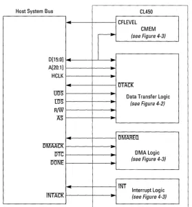
4
Host Interface
The host interface on the CL450 is designed to interface to a variety of general-purpose microprocessors. While it is optimized for connection to members of the 680XO microprocessor family, it also connects easily to the 80X86 family and other host processors.
The host processor can directly access any CL450 register or local DRAM location by reading and writing to specific addresses. Com-pressed video data transfers are performed by writing the data into the CMEM on-chip memory using either processor writes or DMA trans-fers. The CL450 host bus interface supports both vectored and polled in-terrupts.
This chapter is organized into the following sections which describe how the host interface is used:
o 4.1: Overview
o 4.2: Local DRAM or Register Read