A First Principles Simulation Framework for the
Interactions between a Si(001) Surface and a Scanning
Probe
Dung Q. Ly, Charalampos Makatsoris*
School of Engineering and Design, Brunel University, London, UK. Email: *[email protected]
Received May 10th, 2012; revised June 13th, 2012; accepted June 29th, 2012
ABSTRACT
By means of total energy calculations within the framework of the local density approximation (LDA), the interactions between a silicon Si(001) surface and a scanning probe are investigated. The tip of the probe, comprising 4 Si atoms scans along the dimer lines above an asymmetric p(2 × 1) surface, at a distance where the chemical interaction between tip-surface is dominant and responsible for image resolution. At that distance, the tip causes the dimer to toggle when it scans above the lower atom of a dimer. The toggled dimers create an alternating pattern, where the immediately adja-cent neighbours of a toggled dimer remain unchanged. After the tip has fully scanned across the p(2 × 1) surface, causes the dimers to arrange in a p(2 × 2) reconstruction, reproducing the images obtained in scanning probe experiments. Our modelling methodology includes simulations that reveal the energy input required to overcome the barrier to the onset of dimer toggling. The results show that the energy input to overcome this barrier is lower for the p(2 × 1) surface than that for the p(2 × 2) or c(4 × 2) surfaces.
Keywords: DFT; Si(001)-p(2 × 1), p(2 × 2), c(4 × 2); Scanning Probe Microscopy; Phase Transitions; Dimer Toggling
1. Introduction
When silicon is cleaved in the (001) direction, each atom on the surface has two dangling bonds. In an attempt to reduce the surface energy, these atoms bond in pairs, forming dimers and by doing so eliminate one of the two dangling bonds per atom. It is well known that surfaces with buckled, asymmetric dimers have even lower surface energy compared to those with unbuckled, symmetric dimers. Depending on the buckling direction of the dimers, the following three reconstructed surfaces can be ob-tained: 1) p(2 × 1) surface which has all dimers buckled in the same direction; 2) p(2 × 2) surface with neighbour-ing dimers in each row buckled in the opposite direction and neighbouring dimers in a line normal to the dimer row are buckled in the same direction, and finally; 3) c(4 × 2) surface with neighbouring dimers buckled in alternat-ing directions both along and normal to the dimer row.
Determining and manipulating arrangements of atoms on the Si(001) surface by a scanning probe microscopy (SPM) has been an ongoing issue for a long time. Ex-perimental studies at low temperature using scanning tunnelling microscopy (STM) [1-3] and atomic force microscopy (AFM) [4,5] have shown that the c(4 × 2)
geometry is the most stable of all possible reconstructions of the Si(001) surface. When the temperature is increased the c(4 × 2) arrangement of the buckled dimers becomes disordered and a new phase with p(2 × 1) periodicity is obtained. A reason for this is the “flip-flop” motion of the buckled dimers due to thermal excitation. Increasing the temperature, experiments with STM and AFM at room temperature resolve this surface with a symmetric p(2 × 1) structure [6,7]. Those observations are due to the thermally activated “flip-flop” motion of the dimers. Re-sults from low energy electron diffraction show that an order-disorder phase transition takes place at tures of about 200 K [8]. Below this transition tempera-ture the buckled dimers are stable in the c(4 × 2) ordering. Above the transition temperature the thermally activated dimer “flip-flop” motion results to the symmetric p(2 × 1) ordering. This dependence of the phase ordering on tem-perature has been long accepted until recent results ob-tained at sufficiently low temperatures at which it was believed a stable phase c(4 × 2) would be obtained, chal-lenged that assumption. In particular these experiments showed that at temperatures as low as 5 K not only the c(4 × 2) phase can be observed, but other phases such as p(2 × 1) and p(2 × 2) can also be observed.
*
Indeed, observations made by an AFM by Suzuki et al.
[4] involve images of the Si(001) surface at 120 K and 50 K [4] have found that the c(4 × 2) arrangements largely covered the scanning area at 120 K, however, when the temperature was decreased to about 50 K the area cov-ered by p(2 × 2) increased. When lowering the tempera-ture to 5 K and using the same AFM protocol, Uozumi et al. [5] observed asymmetric dimers with antiparallel “zig-zag”-like patterns, a characteristic of the c(4 × 2) geome-try, covered mainly the area. Two other arrangements, namely the p(2 × 2) and the p(2 × 1) were also observed. Further observations in STM experiments at low tem-peratures in the region of 20 K showed a symmetric p(2 × 1) structure. At such temperatures asymmetric dimers were only observed near defects [9]. The same
mecha-nism was also obtained by Yokoyama et al. [7] using
STM experiments at even lower temperatures in the re-gion of 5 K. In these experiments they found out that the observation of symmetric p(2 × 1) structure was due to the anomalous dynamical flipping of the buckled dimers of c(4 × 2).
A number of research groups have performed experi-mental studies to explain the behaviour of atoms on the Si(001) surface induced by a scanning probe [3,10-12]. In such experiments they focused on three parameters that were known to affect the arrangement of atoms on the work surface, namely the bias voltage, the tunnelling current and the tip-sample interaction. All these experi-ments investigated the behaviour of Si(001) under dif-ferent conditions using difdif-ferent protocols. However, they do not offer an explanation of this behaviour in the pres-ence of the tip. It is thus highly desirable to develop first principles based modelling approaches to understand this behaviour of the Si(001) surface in the presence of a scanning probe and guide the design of experiments. It is therefore the aim of this paper to develop such a frame-work to simulate typical imaging protocols with SPM by systematically calculating tip-surface interactions along scanning probe trajectories and ultimately attempt to ob-tain a comprehensive understanding and a guideline for experiment design about how the tip affects the arrange-ment of atoms on the surface.
The tip-surface interaction has attracted much atten-tion from the theoretical community aiming at explaining surface behaviour of different configurations of Si(001) surface [13-18]. Earlier theoretical work in this area has shown how covalent chemical interactions between the dangling bonds of the apex atom of a Si tip and the sur-face atoms introduce dominant forces which are respon-sible for atomic resolution and image contrast. Our pre-vious results demonstrated that when the tip-surface
dis-tance is about 5 Å or higher, the chemical interaction
between them is too weak therefore none of the atoms on the surface can be clearly imaged. By reducing the tip-
surface distance to about 4 Å, its chemical interaction increases rapidly and atoms on the surface are clearly imaged. In addition it was shown how the direction of scanning plays an important role in observing atoms on the surface [17].
In this work we do not just perform calculations by placing the tip at just a few key positions over a confined model of a surface. We rather employ an extended sur-face in our model, not considered in earlier studies, and determine surface reconstructions as a function of tip position relative to the surface. Furthermore, scanning probe trajectories are simulated by advancing the tip in a stepwise manner as a real life tip would and perform qua-sistatic calculations to obtain force, energy landscape and surface reconstruction as explained in detail in the fol-lowing section. These are key features of our modelling framework that can allow more faithful representation of real life scanning probe trajectories and by doing so pro-vide better insight into the tip-surface interactions to in-form imaging experiments. There is a distinctive gap in the literature as most theoretical work in this area is based on the approaches which involve considerably re-duced size models and not tip trajectories mentioned ear-lier. We use our modelling framework to investigate the phase transitions that result from the interaction with the scanning probe, following typical trajectories above an asymmetric p(2 × 1) surface at a close distance to the surface. We extend our study to two additional surface reconstructions, namely the p(2 × 2) and c(4 × 2) sur-faces, to provide a complete investigation and elucidate an understanding of how the probe manipulates atoms on the surface which have led to the observations made in experiments such as those by Sugimoto et al. [19-21].
2. Modelling and Computational
Methodology
layer of the slab and the H atoms are always kept fixed during the calculations. The slab is chosen thick enough so that only atoms on the top layers can reconstruct and atoms on the lower layers remain at their bulk positions. Since we only consider tip-surface interactions and aim to completely avoid interaction between the tip and the bottom layers so in the supercell there is a vacuum gap between the tip and the bottom layer of the next supercell that is thick enough to avoid this interaction happening. Using a vacuum gap of 8 Åwill satisfy that requirement. The unit cell which contains the slab, the tip and the vac-uum gap is shown in Figure 1(a).
Throughout the calculations, total energy and atomic forces are calculated using density functional theory [22], which is implemented in the CASTEP code [23]. Results reported in [17] showed that in general both local density approximation (LDA) [24] and generalised gradient ap-proximation (GGA) [25] for the exchange-correlation term for this system led to the same conclusion. There-fore in the present work we employ only the LDA meth- od. Ultrasoft psuedopotentials are used for the electron- ion interaction. A plane-wave basis set for the electron wave function with cut-off energy of 450 eV is used. Integrations in the Brillouin zone are performed using special k-points generated with 2 × 2 × 1 Monkhurst-Pack grid. It is important to note that results such as total en-ergy difference between different reconstructed surfaces, which we will show in the next section, are very close therefore special care was taken in using parameters such as energy cut-off, k-points etc. These values were chosen after extensive convergence calculations until final results were independent of the choice of those values. Atomic relaxations have been performed via a conjugate gradient
scheme until the energy change (ΔE) between
subse-quent iterations of structural optimisation became less than 1 × 10⁻⁵ eV/atom, while the maximum forces (Fmax)
acting on the atoms were less than 1 × 10⁻² eV/A. The
energy tolerance (δE) between subsequent self-consistent iterations was less than 1 × 10⁻⁶ eV/atom.
Two modes of interaction between the tip and the sur-face are considered in this paper. The first mode is con-cerned with calculations at a fixed tip-surface distance of 4 Å—the vertical distance from the apex atom to the
plane that contains adatoms, shown in Figure 1(a). At
this tip-surface distance the interaction between them is dominated by the covalent chemical interaction which is responsible for atomic resolution and image contrast [16, 17,26]. The tip scans above dimers along the dimer line throughout the whole surface in steps of 0.5 Å. The sec-ond mode is concerned with calculations relating to ver-tical displacements of the tip from the vacuum region towards a lower atom of a dimer. In this mode each step
takes place at 0.2 Å intervals. However, at tip-surface
distances where dimers start to flip, for more accurate
results, the simulation steps have a much shorter interval
of 0.05 Åbetween them.
In each mode, total energies and normal forces are de-termined in a stepwise, quasistatic manner by making small movements of the tip either normal or parallel to the surface. At each step, the apex atom of the tip and atoms in the slab (except atoms on the bottom layer and H atoms which are kept fixed) are allowed to fully relax to their equilibrium positions for that particular tip posi-tion. The optimised surface structure obtained at the nth step is then used as an input (or “seed” structure) for the (n + 1)th step calculations.
3. Results and Discussion
3.1. p(2 × 1) to p(2 × 2) Phase Manipulation
In this section we report the results obtained when the tip scans across an asymmetric p(2 × 1) surface at a distance of 4 Å. The tip is displaced from region A to region B in three different scans, indicated by S1, S2, S3 in Figure 1(a). In Figure 1(b) we show a top-view for these three different scans over the first three layers. The results ob-tained from these scans are shown in Figures 2 and 3.
In scan S1 the tip is displaced from position A1 to po-sition B1 as shown in Figure 2. Initially the tip is at po-sition with coordinates (x, y, z) = (3.34 Å, 3.84 Å, 13.13 Å) with respect to the supercell’s coordinate frame. At this position of the tip the interaction between the tip and
(a) (b)
the lower atom of coordinates (x, y, z) = (4.94 Å, 3.84 Å, 8.42 Å) is still too weak to cause the dimer to flip. When the tip translates further for about 0.5 Åalong the direc-tion of the scan, there is a strong attractive force between the apex atom of the tip and that lower atom, causing it to move up towards the tip. At this position the dimer starts to flip.
Once the dimer flips to its new configuration, it re-mains in this configuration for the duration of the scan thus deforming the surface to this configuration perma-nently. It remains in this configuration even when the tip is above the “new” lower atom. This behaviour can be explained as follows: when the dimer flips the total en-ergy is lowered by 0.17 eV compared to that before flip-ping taking place. This value is obtained by an optimisa-tion calculaoptimisa-tion for a p(2 × 1) surface without the pres-ence of the probe but having one flipped dimer. This im-plies that, when the tip is above the “new” lower atom, in order to cause the dimer to flip back to its original con-figuration, it requires an energy gain that exceeds 0.17 eV. However, with the presence of the probe at a dis-tance of 4 Åabove the surface, or 4.7 Åabove the “new” lower atom, the energy input into the system as a result of the interaction between the tip and the surface is only 0.11 eV. This energy gain is not strong enough to over-come that barrier and cause the dimer to flip back to its original configuration.
[image:4.595.57.287.480.699.2]Further along the scan direction closer to the next row in region B, in particular position B1 in Figure 2, the dimer there flips too when the the tip is above the lower atom of that dimer. This dimer also remains in its new
Figure 2. The surface structure at the end of the first scan (S1), from A1 to B1. The newly flipped dimers are presented in the dark-gray balls.
configuration even when the tip is displaced further away from the dimer along the scan direction. It is important to note that the dimer in the second row starts to flip even at a position of the tip at 10.94 Åalong the x direction and as far as ~1.7 Ålaterally ahead the lower atom at 12.63 Å along the x direction. This position of the tip is much further away from the lower atom, about 0.6 Å, than the position of the tip with respect to the lower atom in the first row at which the dimer flips. This difference is due to the fact that the system is more stable when dimers in the same row are oriented in alternation in opposing di-rections. When a dimer in the second row flips not only it lowers the surface energy by orientating opposite to the dimers next to it but also forms with the flipped dimers in the first row a local p(2 × 2) structure which is more sta-ble than the p(2 × 1) structure. One can conclude that in a p(2 × 1) surface a flipped dimer lowers the energy barrier to flipping the dimer next to it in the next row compared to that of a perfect p(2 × 1) surface.
The next scan, labeled as S2, represents the displace-ment of the tip from position A2 to position B2 shown in the Figure 1(a). Throughout this scan no dimer flipping takes place. The reason is that the energy required to ex-cite the dimer and cause it to flip is greater in the p(2 × 2) surface compared to that in the p(2 × 1) surface. How-ever, at a tip-surface distance of h = 4 Åthe interaction between the tip and the surface is too weak to overcome the energy barrier to the onset of flipping in the local p(2 × 2) structure.
In the final scan S3, which represents a translation of the tip from position A3 to position B3 (shown in Figure 3), flipping of the dimer does occur when the tip scans over the lower atoms. This is the same behaviour as in the first scan S1. In this scan flipping takes place when the tip is at a position with coordinates (3.34 Å, 11.52 Å, 13.13 Å)—at about 1.6 Åalong the x direction and above the lower atom with coordinates (4.94 Å, 11.52 Å, 8.42 Å). So it clearly shows that the first toggled dimer in the scan S1 not only affects, reduces the toggling energy barrier, for the immediate neighbouring dimer in the ad-jacent row but also to the following nearest neighbouring dimers on the same row.
After the tip has scanned the whole surface a complete phase transition from p(2 × 1) to p(2 × 2) takes place as
shown in Figure 3. A structural optimisation is
performing an optimisation calculation, the c(4 × 2)
sur-face is obtained, shown in Figure 4. The calculations
show that this is the most stable surface of Si(001). The energy per dimer of this surface is 3 meV lower than that of the p(2 × 2) surface. Our results confirm the computa-tional results obtained by other groups [15,18].
From an AFM imaging point of view, it has been shown that in lateral scans the variations of the energy and the force have the same trend and the energy or the force distribution can be considered as a qualitative pre-diction of the AFM image in the frequency shift mode
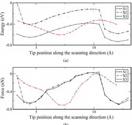
[16,17]. In Figure 5 the total energy and the normal
force as functions of the tip positions are shown as the tip translates along the direction of the scan from region A to B as discussed above. The force at each scanning step is calculated by summing the forces on all fixed atoms
(a) (b)
Figure 3. (a) The surface structure at the end of the third scan (S3), from A3 to B3. In this scan we observe again dimer flipping. The newly flipped dimers, together with the ones previously flipped in scan S1, are shown as dark gray balls. At the end of this scan the structure has completely transformed into a new structure, the Si(001)-p(2 × 2) struc-ture. This new surface remains stable even after the scan-ning probe is completely retracted; (b) Top-view of the first 4 layers of the p(2 × 2) structure (here we separate the first layer into two layers, one layer for adatoms and the other for lower atoms).
(a) (b)
Figure 4. (a) A new surface is obtained after all dimers in one row are flipped and then structural optimisation is performed. The new surface obtained is the Si(001)-c(4 × 2); (b) Top-view of the first 4 layers of the c(4 × 2) structure.
(a)
(b)
Figure 5. (a) Total energies and (b) normal forces as func-tions of tip position along the scanning direction for each of the three different scans.
(H and Si atoms) of the tip. From these curves we clearly see that the energies and the forces follow a similar trend and are nearly the same for both S1 and S3 scans. They have a minimum in energy (or maximum in the normal force) when the tip is above the lower atom of the dimer causing it to flip. When the dimer flips, the lower atom which now becomes the adatom is closer to the tip. The strong interaction between them results to the maximum in the normal force. In scan S2 there is no dimer flipping therefore the strongest interaction occurs when the tip is above the adatoms of the dimmers.
3.2. Comparison of p(2 × 1), p(2 × 2) and c(4 × 2) Surfaces
Bond lengths of dimers and back bonds, as well as buck-ling for the first 6 layers of three different surfaces ob-tained in our work are shown in Tables 1 and 2. Results obtained from experimental observations [27,28] are in-cluded for comparison. In general, our results are in agreement with results obtained by those groups. In par-ticular dimer bond lengths, buckling heights—or buck-ling angles—of p(2 × 2) and c(4 × 2) are nearly the same with small differences by only a few percent.
The lengths between a topmost atom on the first layer of the surface and atoms on the layers beneath it are in very good agreement between our results and the results
obtained by LEED experiments [27,28]. In Table 2 we
[image:5.595.308.539.83.302.2] [image:5.595.57.286.288.451.2] [image:5.595.58.289.586.684.2]Table 1. Bond-length, buckling height, buckling angle between 2 atoms of a dimer for three different reconstructed surfaces obtained in this work and compared to the experimental results in [27,28] (shown in square brackets). The energy difference per dimer between p(2 × 1) and the other surfaces is also shown.
Surface Bond length (Å) Buckling height (Å) Buckling angle (˚) Difference (eV/dimer)
p(2 × 1) 2.267 [2.240] 0.713 [0.690] 18.331 [17.941] 0.000
p(2 × 2) 2.314 0.744 18.755 0.062
c(4 × 2) 2.308 [2.407] 0.744 [0.740] 18.827 [17.905] 0.065
Table 2. Z-coordinate of Si atoms for the reconstructed Si(100)-p(2 × 1), p(2 × 2), c(4 × 2) surfaces obtained by our calcula-tions and compared with LEED measurements [27,28]. The numbers on the far left column represent the labels of different atom positions of the first 6 layers. The same labels are also used in Figures 1, 3, 4.
Si-atom p(2 × 1) Ref. [28] p(2 × 2) c(4 × 2) Ref. [27]
1 0.000 0.000 0.000 0.000 0.000 2 0.713 0.690 0.744 0.746 0.740 3 1.331 1.430 1.439 1.439 1.457 4 1.406 1.440 1.440 1.439 1.457 5 2.620 2.630 2.674 2.674 2.675 6 2.894 3.010 2.968 2.966 3.015 7 4.022 4.080 4.080 4.060 4.112 8 4.215 4.340 4.294 4.293 4.342 9 5.488 5.570 5.551 5.539 5.540 10 5.489 5.610 5.554 5.566 5.580
11 6.865 --- 6.929 6.929 6.927
labeled 2 to 11 and atom labeled 1. The labels from 1 to 11 are also shown in Figures 1, 3 and 4. Most of the at-oms on these layers for these three surfaces are buckled in the same way except atoms on the second and the fifth layers. On the fifth layer, there is a similar ordering of atoms labeled 9 and 10 in p(2 × 1) and p(2 × 2), but in c(4 × 2) the ordering of atoms labeled 9 and 10 is re-versed from that of p(2 × 1) or p(2 × 2). However, in the fifth layer towards the inner layers, atoms buckled rela-tive to its bulk positions are very small and can be ne-glected. In the second layer, it is interesting to observe the similarity between p(2 × 2) and c(4 × 2) structures and how they differ to the p(2 × 1) structure. In p(2 × 2) or c(4 × 2) structures there is virtually no buckling be-tween atoms labeled 3 and 4. This could be due to the fact that dimers on the first layer are arranged alterna-tively in opposite directions hence it compensates for each other and does not favourably induce any atom be-low it to be buckled. However, in the p(2 × 1) case atoms on second layer are buckled by 0.1 Å, this small buckling is due to the buckled dimerization in the first layer.
3.3. Surface Manipulations with Vertical Tip Displacements
In the previous sections we discussed that an external energy which is sufficient to overcome an energy barrier is required to cause a dimer in a p(2 × 1) surface to flip. During an AFM scan, this external energy is provided by the scanning probe when it is sufficiently close to the
surface. There is a certain distance between the scanning probe and the surface at which the interaction is strong enough to overcome the energy barrier and flip the dimer. To determine this distance, the energy and the force are obtained by translating the tip in steps of 0.2 Åfrom the vacuum region where there is no tip-surface interaction towards the lower atom of a dimer in each of the three surfaces, p(2 × 1), c(2 × 2) and c(4 × 2) (see Figure 6). In the region where dimers undergo flipping the distance between each step is reduced to 0.05 Å. Without loss of generality, the system considered in these calculations is reduced to a unit cell comprising 4 dimers arranged in two rows.
The results show that, for the p(2 × 1) surface the dimer flips when the tip is at a distance h ~ 4.10 Å. For p(2 × 2) and c(4 × 2) surfaces flipping occurs at distances
h ~ 3.90 Åand 3.80 Å, respectively. At those distances h
for each of those surfaces the energies due to the tip- surface interactions that overcome the energy barriers are 0.207 (eV), 0.268 (eV) and 0.318 (eV), respectively. It
therefore demonstrates that tip-surface distance h at
which a dimer flips in thep(2 × 1) surface is higher than that of p(2 × 2) and c(4 × 2). Thus, for hc(2 1)c ,
c p(2 2)
h and hc(4 2)c being the critical tip-surface distances for
these three surfaces at which dimers flip, one can observe that hp(2 1)c hp(2 2)c hc(4 2)c . Similarly, for
c p(2 1)
E ,Ep(2 2)c
and Ec(4 2)c being the energy barriers then
c c
p(2 1) p(2 2)
E E
c c(4 2)
E
. This result is in agreement with results by
[image:6.595.56.539.224.370.2]strained energy minimization calculations. Furthermore, it is worthwhile noting the hysteresis in the energy and normal force curves when the tip is at the threshold dis-tance above a lower atom, Figures 6(a) and (b). At this threshold, a sudden increase in the tip-surface interaction occurs as the lower atom moves closer to the tip during dimer flipping. Meanwhile, when the tip scans perpen-dicularly in an attractive region above an adatom no dimer flipping takes place therefore no hysteretic behav-iour is observed in this scan. This behavbehav-iour can be seen in Figure 6(c) showing the energy curve during vertical tip displacements above an adatom.
In Figure 7 we show different surface structures ob-tained at different tip heights, h, above a lower atom for all three surfaces considered in this paper. At h = 8.0 Å there is no interaction between the tip and the surface, therefore the energy of the system is calculated by a straightforward summation of energies of the tip and the surface. As the tip is brought closer to the surface at a distance h = 3.4 Å, dimer flipping does take place in all surfaces considered. At this distance we observe similar behaviour in all surfaces where dimers in one row buck-led in the same direction while dimers in other rows buckled in opposite directions in alternation. This results
(a)
(b)
(c)
[image:7.595.310.538.84.187.2]Figure 6. (a) Total energies and (b) normal forces as func-tions of tip-surface distance, h, when the tip is displaced vertically from the vacuum region towards the lower atom of a dimer for each of the three different surfaces p(2 × 1), p(2 × 2), c(4 × 2); (c) Energy curve when the tip scans ver-tically above an adatom in the p(2 × 1).
Figure 7. Surface structures of p(2 × 1), p(2 × 2), c(4 × 2) at various tip-surface distances, h, when the tip is displaced vertically from the vacuum region towards a lower atom. The direction of the scan is denoted by the arrows.
to an equal in energy in all surfaces, as can be seen in
Figure 6(a) for h in the region of 3.4 Å. Further reduc-tion of h to 1.4 Åthere is a repulsive interaction between the tip and the surface. In this case we can observe that the adatom below the tip is pushed downwards leading to a symmetric dimer. The same behaviour was observed by Cho et al. [13].
4. Conclusions
In this paper we presented a modelling framework that employes total energy calculations to study the interac-tions between a Si tip and surface. With this framework we conducted a systematic study of the phase transitions from p(2 × 1) to p(2 × 2) reconstructions which are the result of the interactions between the surface and the Si scanning probe. In the simulations the tip scans along an initial p(2 × 1) surface at a constant height of 4 Åabove the surface. The tip scans the surface in a direction nor-mal to the dimer rows. As a result of the interactions be-tween the tip and the surface the dimers along the first scan toggle and locally form a p(2 × 2) structure. The formation of the p(2 × 2) structure reduces the total en-ergy of the system and increases the enen-ergy barrier that prevents the surface to form its original configuration, causing a permanent deformation of the surface. During the second scan along the next dimer line, which has a local configuration of p(2 × 2), no dimer flipping is ob-served. This is due to the tip-surface interaction is not strong enough to overcome the energy barrier required to cause the dimer to flip. In a third scan over the next
dimer line which has a local p(2 × 1) structure, dimer
flipping is observed again. After the tip has completely scanned the surface, a complete phase transition from p(2 × 1) to p(2 × 2) has taken place with an energy per dimer of the p(2 × 2) structure being lower than that of the p(2 × 1) structure by 0.062 eV.
[image:7.595.56.289.386.667.2]of the tip-surface distance, at which the tip causes the dimers to flip, is higher for the p(2 × 1) structure than that of the p(2 × 2) and c(4 × 2) structures. It thus follows that the energy barrier is lower for the p(2 × 1) structure than that of the p(2 × 2) and c(4 × 2) structures. These results provide an understanding of the behaviour of the Si(001) surface when a tip is present and can therefore provide a guideline in designing experimental protocols involving ato- mic manipulations with SPM on this type of surface such as those pioneered by the groups of Su-gimoto et al. [19,21] and Oyabu et al. [29-31]. Finally, with the capability of modern instruments to control with atomic precision tip trajectories and with future model- based support using simulation frameworks such as the one described here, one can envisage that scanning probes can be used as a tool not only to manipulate atoms on the surface but also to “pick and place” single atoms or small molecules and grow almost any arbitrary struc-ture on a given surface in the fustruc-ture [32].
5. Acknowledgements
This work has been supported by the UK Engineering and Physical Sciences Research Council (EPSRC) under contract EP/F009801/1 and Brunel University’s BRIEF award scheme. The authors would like to thank the School of Engineering and Design for purchasing our computing cluster to support research in this area. All simulations were performed on the cluster comprising 64 processors at Brunel University.
REFERENCES
[1] R. A. Wolkow, “Direct Observation of an Increase in Buckled Dimers on Si(001) at Low Temperature,” Physi- cal Review Letters, Vol. 68, No. 17, 1992, pp. 2636-2639. doi:10.1103/PhysRevLett.68.2636
[2] H. Tochihara, T. Amakusa and M. Iwatsuki, “Low-Tem- perature Scanning-Tunneling-Microscopy Observations of the Si(001) Surface with a Low Surface-Defect Density,” Physical Review B, Vol. 50, No. 16, 1994, pp. 12262- 12265. doi:10.1103/PhysRevB.50.12262
[3] T. Mitsui and K. Takayanagi, “Extrinsic Structure Changes by STM at 65 K on Si(001),” Physical Review B, Vol. 62, No. 24, 2000, pp. R16251-R16254.
doi:10.1103/PhysRevB.62.R16251
[4] K. Suzuki, M. Iwatsuki, S. Kitamura and C. B. Mooney, “Development of Low Temperature Ultrahigh Vacuum Atomic Force Microscope/Scanning Tunneling Micro- scope,” Japanese Journal of Applied Physics, Vol. 39, 2000, pp. 3750-3752. doi:10.1143/JJAP.39.3750
[5] T. Uozumi, Y. Tomiyoshi, N. Suehira, Y. Sugawara and S. Morita, “Observation of Si(100) Surface with Noncon- tact Atomic Force Microscope at 5 K,”Applied Surface Science, Vol. 188, No. 3-4, 2002, pp. 279-284.
doi:10.1016/S0169-4332(01)00939-4
[6] R. J. Hamers, R. M. Tromp and J. E. Demuth, “Scanning Tunneling Microscopy of Si(001),” Physical Review B, Vol. 34, No. 8, 1986, pp. 5343-5357.
doi:10.1103/PhysRevB.34.5343
[7] K. Yokoyama, T. Ochi, A. Yoshimoto, Y. Sugawara and S. Morita, “Atomic Resolution Imaging on Si(100)2 × 1 and Si(100)2 × 1:H Surfaces with Noncontact Atomic Force Microscopy,” Japanese Journal of Applied Physics, Vol. 39, 2000, pp. L113-L115. doi:10.1143/JJAP.39.L113
[8] T. Tabata, T. Aruga and Y. Murata, “Order-Disorder Transition on Si(001): c(4 × 2) to (2 × 1),” Surface Sci- ence, Vol. 179, No. 1, 1987, pp. L63-L70.
doi:10.1016/0039-6028(87)90114-2
[9] Y. Kondo, T. Amakusa, M. Iwatsuki and H. Tokumoto, “Phase Transition of the Si(001) Surface Below 100 K,” Surface Science, Vol. 453, No. 1-3, 2000, pp. L318-L322. doi:10.1016/S0039-6028(00)00391-5
[10] K. Sagisaka, D. Fujita and G. Kido, “Phase Manipulation between c(4 × 2) and p(2 × 2) on the Si(100) Surface at 4.2 K,” Physical Review Letters, Vol. 91, No. 14, 2003, pp. 146103-146106. doi:10.1103/PhysRevLett.91.146103 [11] M. Ono, A. Kamoshida, N. Matsuura, E. Ishikawa, T. Egu-
chi and Y. Hasegawa, “Dimer Buckling of the Si(001)2 × 1 Surface Below 10 K Observed by Low-Temperature Scan- ning Tunneling Microscopy,” Physical Review B, Vol. 67, No. 20, 2003, pp. 201306-201309.
doi:10.1103/PhysRevB.67.201306
[12] S. Yoshida, T. Kimura, O. Takeuchi, K. Hata, H. Oigawa, T. Nagamura, H. Sakama and H. Shigekawa, “Probe Ef- fect in Scanning Tunneling Microscopy on Si(001) Low- Temperature Phases,” Physical Review B, Vol. 70, No. 23, 2004, pp. 235411-235421.
doi:10.1103/PhysRevB.70.235411
[13] K. Cho and J. D. Joannopoulos, “Flipping Silicon Dimers on Si(100) Using Scanning Tip Microscopy: A Theoreti- cal Investigation,” Physical Review B, Vol. 53, No. 8, 1996, pp. 4553-4556. doi:10.1103/PhysRevB.53.4553
[14] Y. J. Li, H. Nomura, N. Ozaki, Y. Naitoh, M. Kageshima, Y. Sugawara C. Hobbs and L. Kantorovich, “Origin of p(2 × 1) Phase on Si(001) by Noncontact Atomic Force Microscopy at 5 K,” Physical Review Letters, Vol. 96, No. 10, 2006, pp. 106104-106107.
doi:10.1103/PhysRevLett.96.106104
[15] L. Kantorovich and C. Hobbs, “Probing the Si(001) Sur- face with a Si Tip: An ab Initio Study,” Physical Review B, Vol. 73, No. 24, 2006, pp. 245420-245431.
doi:10.1103/PhysRevB.73.245420
[16] R. Perez, I. Stich, M. C. Payne and K. Terakura, “Sur- face-Tip Interactions in Noncontact Atomic-Force Mi- croscopy on Reactive Surfaces: Si(111),” Physical Re- view B, Vol. 58, No. 16, 1998, pp. 10835-10849. doi:10.1103/PhysRevB.58.10835
[17] D. Q. Ly, L. Paramonov and C. Makatsoris, “First Princi- ples Studies of an Si Tip on an Si(100)2 × 1 Recon- structed Surface,”Journal of Physics: Condensed Matter, Vol. 21, No. 18, 2009, pp. 185006-185013.
doi:10.1088/0953-8984/21/18/185006
Injection,” Physical Review Letters, Vol. 93, No. 3, 2004, pp. 036101-036104. doi:10.1103/PhysRevLett.93.036101
[19] Y. Sugimoto, M. Abe, S. Hirayama, N. Oyabu, C. Cus- tance and S. Morita, “Atom Inlays Performed at Room Temperature Using Atomic Force Microscopy,” Nature, Vol. 4, No. 2, 2005, pp. 156-159. doi:10.1038/nmat1297
[20] Y. Sugimoto, P. Lou, M. Abe, P. Jelinek, R. Perez, S. Morita and O. Custance, “Chemical Identification of In- dividual Surface Atoms by Atomic Force Microscopy,” Nature, Vol. 446, No. 7131, 2007, pp. 64-67.
doi:10.1038/nature05530
[21] Y. Sugimoto, P. Pou, O. Custance, P. Jelinek, M. Abe, R. Perez and S. Morita, “Complex Patterning by Vertical In- terchange Atom Manipulation Using Atomic Force Mi- croscopy,” Science, Vol. 322, No. 5900, 2008, pp. 413- 417. doi:10.1126/science.1160601
[22] M. C. Payne, M. P. Teter, D. C. Allan, T. A. Arias and J. D. Joannopoulos, “Iterative Minimization Techniques for ab Initio Total-Energy Calculations: Molecular Dynamics and Conjugate Gradients,” Physical Review Letters, Vol. 64, No. 4, 1992, pp. 1045-1097.
doi:10.1103/RevModPhys.64.1045
[23] S. J. Clark, M. D. Segall, C. J. Pickard, P. J. Hasnip, M. J. Probert, K. Refson and M. C Payne, “First Principles Methods Using CASTEP,” Zeitschrift fur Kristallogra- phie, Vol. 220, No. 5-6, 2005, pp. 567-570.
doi:10.1524/zkri.220.5.567.65075
[24] J. P. Perdew and A. Zunger, “Self-Interaction Correction to Density-Functional Approximations for Many-Electron Systems,” Physical Review B, Vol. 23, No. 10, 1981, pp. 5048-5079. doi:10.1103/PhysRevB.23.5048
[25] J. P. Perdew, K. Burke and M. Ernzerhof, “Generalized Gradient Approximation Made Simple,” Physical Review Letters, Vol. 77, No. 18, 1996, pp. 3865-3868.
doi:10.1103/PhysRevLett.77.3865
[26] A. Sweetman, S. Jarvis, R. Danza, J. Bamidele, S. Gan-
gopadhyay, G. A. Shaw, L. Kantorovich and P. Poriaty, “Toggling Bistable Atoms via Mechanical Switching of Bond Angle,” Physical Review Letters, Vol. 106, No. 13, 2011, pp. 136101-136104.
doi:10.1103/PhysRevLett.106.136101
[27] T. Shirasawa, S. Mizuno and H. Tochihara, “Structural Analysis of the c(4 × 2) Reconstruction in Si(001) and Ge(001) Surfaces by Low-Energy Electron Diffraction,” Surface Science, Vol. 600, No. 4, 2006, pp. 815-819. doi:10.1016/j.susc.2005.11.031
[28] H. Over, J. Wasserfall, W. Ranke, C. Ambiatello, R. Sawitzki, D. Wolf and W. Moritz, “Surface Atomic Ge- ometry of Si(001)-(2 × 1): A Low-Energy Electron-Dif- fraction Structure Analysis,” Physical Review B, Vol. 55, No. 7, 1997, pp. 4731-4736.
doi:10.1103/PhysRevB.55.4731
[29] N. Oyabu, O. Custance, I. Yi, Y. Sugawara and S. Morita, “Mechanical Vertical Manipulation of Selected Single Atoms by Soft Nanoindentation Using Near Contact Ato- mic Force Microscopy,” Physical Review Letters, Vol. 90, No. 17, 2003, pp. 176102-176105.
doi:10.1103/PhysRevLett.90.176102
[30] N. Oyabu, Y. Sugimoto, M. Abe, O. Custance and S. Morita, “Lateral Manipulation of Single Atoms At Semi- conductor Surfaces Using Atomic Force Microscopy,” Nanotechnology, Vol. 16, No. 3, 2005, pp. S112-S117. doi:10.1088/0957-4484/16/3/021
[31] N. Oyabu, P. Pou, Y. Sugimoto, P. Jelinek, M. Abe, S. Morita, R. Perez and O. Custance, “Single Atomic Con- tact Adhesion and Dissipation in Dynamic Force Micros- copy,” Physical Review Letters, Vol. 96, No. 10, 2006, pp. 106101-106104. doi:10.1103/PhysRevLett.96.106101
[32] R. C. Merkle and R. A. Freitas, “Theoretical Analysis of a Carbon-Carbon Dimer Placement Tool for Diamond Me- chanosynthesis,” Journal of Nanoscience and Nanotech- nology, Vol. 3, No. 4, 2003, pp. 319-324.

![Table 1. Bond-length, buckling height, buckling angle between 2 atoms of a dimer for three different reconstructed surfaces obtained in this work and compared to the experimental results in [27,28] (shown in square brackets)](https://thumb-us.123doks.com/thumbv2/123dok_us/9291578.425381/6.595.56.539.224.370/buckling-buckling-different-reconstructed-surfaces-compared-experimental-brackets.webp)

