I.
II.
III.
T T 7 ~V ..
v.
DISKOS 1070 PRODUCT SPECIFICATION
~
INTRODUCTION A. Purpose
B. General Description C. Features
PRODUCT DESCRIPTION
A. Operational Specifications B. Physical Characteristics C. Controls
D. Environmental Characteristics E •. Reliability
F. Power Requirements DATA INTEGRITY
A. Seek Errors
B. Recoverable Errors C. Non-Recoverable Errors D. Skip Defect
INTERFACE
A. General
B. Address and Command Control C. Serial Data Transfer
D. Physical Interface SUGGESTED DATA FORMAT A. Format Definitions
FIGURES
Figure 1 DISKOS 1070 Disc Drive 5
2 DBUS Transceiver 19
3 Single Line Receiver Gated by Drive Select 20
4 Single End Line Receiver 22
5 Single Line Driver 23
6 Differential Line Drivers & Receivers 24
7 Register Load Timing 26
8 Register Read Timing 27
9 Reset Pulse Width Timing 27
10 Index & Sector Mark Timing 28 11 Write Data & Write Clock Timing 29 12 Read Data & Read Clock Timing 30
13 Record Writing Timing 31
14 Record Reading Timing 32
15 Read & write Transitions During Gaps 34
I. I NTRODUC TI ON
A. Purpose
This specification describes the performance and the physical and electrical characteristics of the PRIAM DISKOS 1070 disc·drive. It provides the necessary information to connect a DISKOS 1070 to a disc drive controller through a microprocessor type of
interface. This document ·provides the reference technical
~ecifications required by OEM users. Interface and detailed
timing data are not included in the short form of this specification.
B. General Description
The DISKOS 1070 uses advanced Winchester and microprocessor technologies to provide users with a low-cost disc drive having high capacity and long-term reliability. A stepper motor drive.n positioner enables the DISKOS 1070 to position Winchester type heads quickly and precisely. These low-force heads assure high data reliability. An advanced 8-inch Winchester-technology disc is driven by a brushless DC motor. The head positioner and carriage, heads, and disc are enclosed in a s~aled,
contamination-resistant chamber to assure high reliability.
A microprocessor provides interface flexibility and monitors drive operation. For example, it controls the power up and down sequencing and a self-test program checks drive performance
during each power up sequence. Any malfunction detected by these tests will prevent drive start-up, reducing the chance of loss of data or damage to the drive.
c.
Features1. 10 megabytes of mass storage at low cost for small system usage.
2. Advanced Winchester technology discs and heads provide efficient and cost-effective data density.
3~ Brushless DC spindle drive motor improves reliability by: a. Accelerating and braking the disc quickly, extending
disc and head life and improving data reliability.
b. Elimination of the belts, pulleys, switches and starting capacitors.
--4. Reserved area on disc surface for head landing and takeoff protects data integrity.
...
J . Package size identical to the ~Industry Standard~ 8-inch
floppy.
6. Light weight--only 20 pounds--reduces cost of installation.
7. Flexible, microprocessor-based interface:
a. Eliminates handshake protocols, freeing valuable processor time.
b. Supports daisy-chained drives and overlapping seeks.
c. Simplifies controller design and allows up to a 25-foot controller cable without the need for additional line drivers and receivers.
8. Microprocessor-controlled self-test protects data and the drive and aids troubleshooting.
9. DC operation permits flexibility of prime power source and ease of battery backup.
10. Skip defect data is stored within the drive, eliminating the need for defect record keeping and manual insertion- of data during system integration.
11. VFO/data separator provided.
12. Selectable sector size: 256 to 1024 bytes, for data area (formatted).
Application notes to aid users in design of controllers for the DISKOS
II. PRODUCT DESCRIPTION
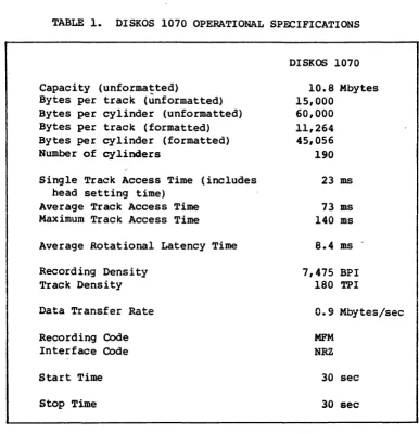
A. Operational Specifications
Operational specifications of the DISKOS 1070 disc drive are shown in Table 1 below.
TABLE 1. DISKOS 1070 OPERATIONAL SPECIFICATIONS
Capacity (unformaEted)
Bytes per track (unformatted) Bytes per cylinder (unformatted) Bytes per track (formatted) Bytes per cylinder (formatted) Number of cylinders
Single Track Access Time (includes head setting time)
Average Track Access Time Maximum Track Access Time
Average Rotational Latency Time
Recording Density Track Density
Data Transfer Rate
Recording Code Interface Code
Start Time
Stop Time
DISKOS 1070
10.S Mbytes 15,000
60,000 11,264 45,056 190
23 IDS
73 ms 140 ms
S.4 ms
7,475 BPI ISO TPI
0.9 Mbytes/sec MFM
NRZ
30 sec
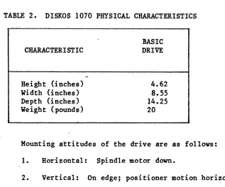
[image:5.613.109.495.147.546.2]B. Physical Characteristics
The physical characteristics of the DISKOS 1070 disc drive are sho~~
in Table 2 below.
TABLE 2. DISKOS 1070 PHYSICAL CHARACTERISTICS
CHARACTERISTIC
Height (inches) Width (inches) Depth (inches) Weight (pounds)
BASIC DRIVE
4.62
8.55
14.25 20
Mounting attitudes of the drive are as follows:
1. Horizontal: Spindle motor down.
2. Vertical: On edge; positioner motion horizontal.
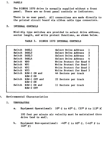
[image:7.612.126.443.113.377.2]C. Controls
D.
1" P~~F.T·S
The DISKOS 1070 drive is normally supplied without a front panel. There are no front panel controls or indicators.
There is no rear panel. All connections are made directly to the printed circuit board via ribbon cable type connectors"
2. INTERNAL CONTROLS
Mini-dip type switches are provided to select drive address, sector length, and write protect functions, as shown below.
TABLE 3. DISKOS 1070 INTERNAL CONTROLS
Switch DSELI Select Drive Address 1
Switch DSEL2 Select Drive Address 2
Switch DSEL3 Select Drive Address 3
Switch DSEL4 Select Drive Address 4
Switch WPO Write Protect for Head 0
Switch WPl Write Protect for Head 1
'Switch
WP2
Write Protect for Head 2Switch WP3 Write Protect for H~ad 3
Switch RSW-l ON and 44 Sectors per track RSW-2 ON
Switch RSW-l OFF and 22 Sectors per track RSW-2 ON
Switch RSW-l ON and 11 Sectors per track RSW-2 OFF
Environmental Characteristics
1. TEMPERATURE
a. Equipment Operational: 100 C to 450 C. (570 F to 1130 F)
100 feet per minute air velocity must be maintained through the drive (end to end).
b. Equipment Non-operational: -400 C to 600 C. (-400 F to
[image:9.612.100.519.68.661.2]2. HUMIDITY
a. Equipment Operational: 10% to 80% relative humidity, with a wet bulb temperature limit of 260 C (780 F) without
condensation.
h. Equipment Non-operational: 10% to 90% without condensation.
3. ALTITUDE
a. Equipment Operational: From 1000 feet below sea level to 7000 feet above sea level.
b. Equipment Non-operational: From 1000 feet below sea level to 40,000 feet above sea level.
E. Reliability
1. MTBF
The DISKOS 1070 has an expected Mean Time Between Failures (MTBF) of 10,000 power-on hours.
2. MTTR
The DISKOS 1070 is designed so that the Mean Time to Repair
(MTTR) is less than 1/2 hour.
3. PREVENTIVE MAINTENANCE
No preventive maintenance is required.
F. Power Requirements
1. DC. POWER REQUIREMENTS
The DISKOS 1070 is provided without a power supply and with the standard microprocessor interface, the following power is
required from the system:
+24 VDC, ~ 5%,5.1 maximum; ripple 500 mv MAX P-P
+ 5 VDC,
.!.
5%,2.5 maximum; ripple 100 mv MAX P-PIII. DATA INTEGRITY
A. Seek Errors
Seek errors result when the head does not reach the correct track, which can be verified by reading the ID field. w~enever such an
error occurs, the drive's track counter must be reset to zero by issuing a RESTORE command to the drive, which will move the head back to cylinder zero. Then a new SEEK command may be issued.
The seek error rate is less than one error in 106 SEEK executions.
B. Recoverable Data Errors
Recoverable read errors result from transient conditions and are usually corrected by simply re-reading. Errors are normally detected by using cyclic redundancy checking (CRC), performed in the disc drive controller. Each field should be terminated with CRC information.
The recoverable read error rate is less than one error in 1010 bits.
C. Non-Recoverable Data Errors
A non-recoverable error is one which persists after several attempts to read the record. This error may be a write error, in which case rewriting the record clears the error. Or, the error may be a disc defect, in which case the error may persist even though the record 1S
rewritten.
The non-recoverable error rate is less than one error in 1013 bits. Errors that are detected and flagged (either by alternate track or skip defect methods) during initialization are not included in determining this error rate.
D. Skip Defect
Recorded on each track between index and the first sector pulse is a short data record containing skip defect information. This record contains the addresses of up to three known defects on the addressed track. Each defect is defined by a two-byte binary address of the byte in which the defect is located; zero indicates no defect.
Th1S information is accessed by initiating a read, coincident with
the front edge of the index pulse, and reading until the leading edge of the first sector pulse. Use of this technique allows automatic defect mapping and alternate sector allocation, rather than the.more commonly used method of providing the user with a written record of the defective areas. The latter method makes it necessary for the user to enter the defective area information manually. A written record is also provided by PRIAM, but it is needed only by customers who wish to retain defect records in their files.
IV. INTERFACE
A. General
PRIAM offers a basic 8-bit bidirectional bus control interface designed to be readily connected to popular 8-bit and l6-bit microprocessors. Across this interface all spindle motor and head positioning controls are passed.
Read and Write Data is passed via synchronous serial-bit NRZ signal lines. The interface provides for the following synchronization signals; INDEX, SECTOR MARK, READ/REFERENCE CLOCK, and WRI TE CLOCK.
Up to four drives may be daisy chained along a single 50
conductor flat ribbon cable. Power is provided via a separate cable.
Each of these interface areas is discussed in the balance of this section in terms of:
1. Address and Command Control
2. Serial Data Transfer
3. Physical Interface
The information contained in the balance of the section is sufficient for the design of a controller for attachment of the DISKOS 1070.
B. Address and Command Control
All cylinder addresses, status information and commands are transferred over the three-state bidirectional DEUS 0 through 7 lines. These eight lines present an open circuit (tri-state) to the controller's bus until activated by DRIVE SELECT. An active DRIVE SELECT combined with RD (Read) sets the DBUS into the transmit mode while DRIVE SELECT combined with an active WR
(Write) sets the DEUS into the receive mode. The information to control the
1.
2.
Control Command Register which receives and stores commands from the controller.
Target Address Register which Receives the eight bits of the desired cylinder address.
3~ Status Register which contains pertinent information about present operation.
4. Current Address Register Lower Byte which contains the eight bits of the current cylinder address or other requested drive parameters.
5. Current Address Register, Upper Byte which is always zero for current address and drive ID information and contains the upper eight bits defining the selected sector size.
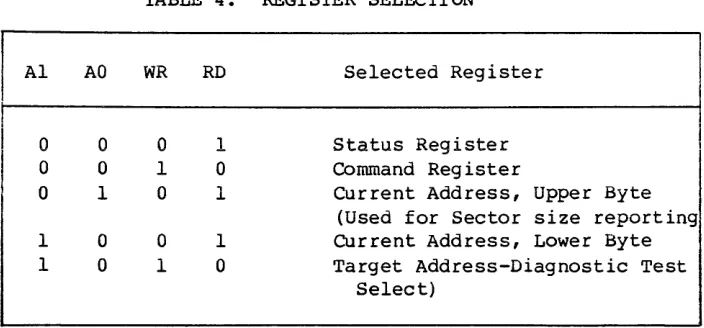
Accessing of the registers is accomplished by a combination of active levels on DRIVE SELECT, RD or WR, and register address lines Al and AO, as shown in Table 4. The Command and Target Address Registers can only receive information and the Status and Current Address Registers can only transmit information.
TABLE 4. REGI STER SELECTION
Al AO WR RD Selected Register
0 0 0 1 Status Register
0 0 1 0 Command Register
0 1 0 1 Current Address, Upper Byte (Used for Sector size reporting 1 0 0 1 Current Address, Lower Byte 1 0 1 0 Target Address-Diagnostic Test
[image:13.612.133.485.358.522.2]Seven Control Commands are used. All are single byte commands and are listed in Table
5.
TABLE 5. COMMAND SUMMARY
COMMAND 7 6
SEQUENCE UP 0 0
SEQUE NCE DOWN 0 0
RESTORE 0 0
SEEK 0 0
FAULT RESET 0 0
READ DRIVE ID 0 0
READ SELECTED 0 0
SECTORS SIZE
1. SEQUENCE UP
BITS 5 4 3
0 0 0 0 0 0 0 0 0 0 0 0 0 0 0 0 1 0 0 1 0
2 1
o
0 0 1 0 1 0 0 1 1 ;1 0 0 1 0 1 0 0 0 0 0 1
The SEQUENCE UP Command causes the disc drive spindle motor to power up. The rotational speed of the disc is monitored, and when the drive is up to speed, the heads are positioned to cylinder zero. The drive will present BUSY status while the SEQUENCE UP is in process. CYLINDER ZERO, SEEK COMPLETE and READY status is set at the successful completion of this
command. WRITE PROTECT and DRIVE FAULT are set if the SEQUENCE UP was unsuccessful.
2. SEQUENCE DOWN
The SEQUENCE DOWN command causes the heads to be positioned to the landing zone and the spindle motor is braked to a stop. WRITE PROTECT status will be set at the completion of this
command.
3. RESTORE
The RESTORE command causes the drive carriage to be repositioned to cylinder zero. The drive RESTORES automatically on SEQUENCE UP, or when a SEEK FAULT is detected. Upon failure of the RESTORE command, the heads will be positioned to the landing
[image:14.613.125.493.102.510.2]4. SEEK
The SEEK cc~~and uses the contents of the Target Address Register for desired cylinder address information. Upon receipt of this command, the drive will go NOT READY and BUSY while moving the carriage to the desired cylinder. When this is complete, the drive will again become READY and SEEK COMPLETE status will be posted. Upon failure of the SEEK co~~and, the drive will RESTORE to cylinder zero and present READY, CYLINDER ZERO and SEEK FAULT status.
5. FAULT RESET
The FAULT RESET command clears both fault condition flip-flops (SEEK FAULT and DRIVE FAULT).
6. READ ID
This command sets the Drive ID code (10 hex) in the Current Address Register. READY status will be reset to the not ready state. In order to bring the drive to the READY state a SEQUENCE UP or RESTORE command must be executed. Thus, the Current Address Register contains the valid current cylinder address if the drive is READY and last requested parameter information if not READY.
7. READ BYTE S PE R SECTOR
This command sets the switch selected number of bytes per sector in the Current Address Registers. There are three possible settings:
1. 340 Bytes per Sector (44 Sectors per Track) Switch RSW-l ON and RSW-2 ON.
2. 680 Bytes per Sector (22 Sectors per Track) Switch RSW-l OFF and RSW-2 ON.
3. 1,360 Bytes per Sector (11 Sectors per Track) Switch RSW-l ON and RSW-2 OFF.
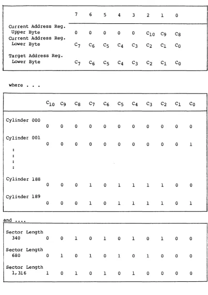
TABLE 6.
Current Address Reg. Upper Byte
Current Address Reg. Lower Byte
Target Address Reg. Lower Byte
where
. . .
CIa C9
Cylind~r 000
I
Cylinder 001Cylinder 188
Cylinder 189
and ••••
I
Sector Length 340Sector Length 680
I
a
a
a
a
a
o
Sector Length
a
a
a
a
a
1
ADDRESS REGISTER BIT DEFINITION
7 6 5 4 3 2 1 a
a a a a a CIO Cg Cs
C., I Cc -u Cc: - . J C4 C., - J c') -&. Cl Cn -v
C7 C6 Cs C4 C3 C2 CI Co
C8 C7 C6 Cs C4 C3 C2 CI Co
a
a aa
a
aa
a
a
a
a
a
a
a
a
a
a
1a 1 a 1 1 1 1 a a
a 1 a 1 1 1 1 a 1
I a 1 a 1 o 1 a a
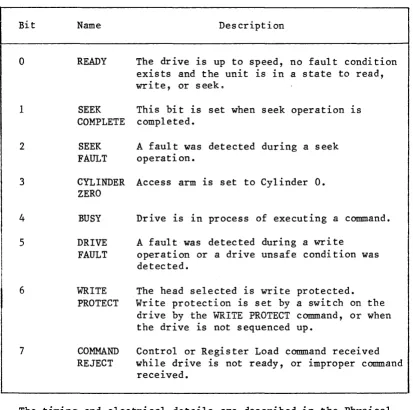
[image:16.613.76.505.59.665.2]The following is a definition of the various bits of the Status Register.
Bit
o
1
2
3
4
5
6
7
TABLE 7. STATUS REGISTER BIT DEFINITION
Name
READY
SEEK
Description
The drive is up to speed, no fault condition exists and the unit is in a state to read, write, or seeke
This bit is set when seek operation is COMPLETE completed.
SEEK FAULT
CYLINDER ZERO
BUSY
DRIVE FAULT
WRITE PROTECT
COMMAND REJECT
A fault was detected during a seek operation.
Access arm is set to Cylinder O.
Drive is in process of executing a command.
A fault was detected during a write
operation or a drive unsafe condition was detected.
The head selected is write protected. Write protection is set by a switch on the drive by the wKITE PROTECT command, or when the drive is not sequenced up.
Control or Register Load command received while drive is not ready, or improper command
received.
[image:17.613.104.517.109.519.2]C. Serial Data Transfer
Several individual signal lines provide timing and status information to facilitate the serial data transfer between the drive and
controller. These signals are:
1. INDEX
A l.9-microsecond pulse that occurs whenever the mechanical index mark is encountered to indicate the, beginning of a track. The
timing is discussed in the Physical Interface section.
2. ~
This signal indicates that the selected drive is ready to read, write, or seek. When this line is false, WRITE, READ and SEEK commands should not be initiated by the controller. However, READY will go false whenever a SEEK command is initiated and remain false until the seek is completed, at which time it will become true again.
READY will be true when the drive is at speed, on cylinder and no fault condition exists.
3 • SECTOR MARK
4.
SECTOR MARK is a 960 nanosecond pulse that occurs at the beginning of each sector. The sector size is selectable by setting mini-dip type switches on the drive. Two mini-dip switches are provided to select sector length. See Table 8 for switch assignment~
TABLE 8. SECTOR LENGTH SWITCH
Switch Switch Sector Length
RSW-l RSW-2
ON ON 340 bytes (44 sectors/track)
OFF ON 680 bytes (22 sectors/track)
ON OFF 1360 bytes (11 sectors/track)
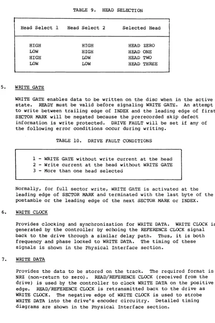
HEAD SELECT 1, HEAD SELECT 2
TABLE 9. HEAD SELECTION
Head Select 1 Head Select 2 Selected Head
HIGH HIGH HE..~D ZERO
LOW HIGH HEAD ONE
HIGH LOW HEAD TWO
LOW LOW HEAD THREE
5. WRITE GATE
WRITE GATE enables data to be written on the disc when in the active state. READY must be valid before signaling WRITE GATE. An attempt to write between trailing edge of INDEX and the leading edge of first SECTOR MARK will be negated because the prerecorded skip defect
information is write protected. DRIVE FAULT will be set if any of the following error conditions occur during writing.
TABLE 10. DRIVE FAULT CONDITIONS
1 - WRITE GATE without write current at the head 2 - Write current at the head without WRITE GATE 3 - More than one head selected
Normally; for full sector write, WRITE GATE is activated at the leading edge of SECTOR MARK and terminated with the last byte of the postamble or the leading edge of the next SECTOR MARK or INDEX.
6. WRI TE CLOCK
Provides clocking and synchronization for WRITE DATA. WRITE CLOCK is generated by the controller by echoing the REFERENCE CLOCK signal back to the drive through a similar delay path. Thus, it is both frequency and phase locked to WRITE DATA. The timing of these
7. WRITE DATA
Provides the
[image:19.613.72.509.36.692.2]8. READ GATE
This signal mus~ be enabled in a gap area (all D's recorded) and at least 8 microseconds before the sync byte. READ GATE enables the VFO clock to synchronize with the information from the read head.
Raising READ GATE during a data record may cause the VFO to
spuriously lock in incorrect phase relationship for correct decoding of recorded information.
7.5
±
0.5 microseconds after the leading edge of READ GATE the READ CLOCK is gated to the READ/REFERENCE CLOCK signals.9. READ/REFERENCE CLOCK
Provides clocking and synchronization for reading and writing data. When READ GATE is not active this signal is the REFERENCE CLOCK which is derived from the crystal oscillator.
7.5
±
0.5 microseconds after the leading edge of READ GATE,READ/REFERENCE CLOCK is switched to the VFO which is phase locked to READ DATA. A change in the READ/REFERENCE CLOCK phase or a spurious pulse may occur when it is switched between the crystal oscillator and VFO clocks.
10. READ DATA
Data from the drive is in serial bits NRZ (non-return to zero) and is synchronized with READ/REFERE~~E CLOCK 7.5
±
0.5 microseconds after the leading edge of READ GATE. READ DATA may not be valid for the first 8 microseconds after the leading edge of READ GATE.D. Physical Interface
All drive signal connections are made via a single 50-pin ribbon cable connector Jl. A second 50-pin connector, J2, is provided for daisy
chaining to another drive or for a terminator attachment at the last drive in the string. Up to four drives may be daisy chained.
Terminator must be installed in connector J2.
A separate connector for DC power is provided.
1. Jl and J2 CONNECTOR
Jl and J2 Connector Pin 1 2 3 4 5 6 7 8 9 10 11 12 13 14 15 16 17 18 19 20 21 22 23 24 25 26 27 28 29 30 31 32 33 34 35 36 37 38 39 40 41 42 43 44 45 46 47 48 49 50 Signal Ground + DBUS 0 + DBUS 1 + DBUS 2 + DBUS 3
+ DBUS
4
+ DBUS 5
+ DBUS 6
+ DBUS 7 Ground - READ GATE Ground - RESET Ground
- WRITE GATE Ground
- RD - WR + AD 1
+ AD 0
Ground
- DRIVE SELECT 1
- DRIVE SELECT 2
- DRIVE SELECT 3 - DRIVE SELECT 4 Ground
Ground
+ 5 VOLTS DC (TERMINATOR POWER) Reserved (No connection)
- HEAD SELECT 2 - HEAD SELECT 1 Ground
- INDEX Ground
- READY
Ground
- SECTOR MARK Ground
+ WRITE DATA - WRITE DATA Ground
+ WRITE CLOCK - WRITE CLOCK Ground
+ READ/REFERENCE CLOCK - READ/REFERENCE CLOCK Ground
2. J3 CONNECTOR
This connector is used to supply DC power to the drive. J3 is a 6-pin AMP MATE-N-LOK Connector, and the recommended mating connector is an AMP
1-480270-0 socket using AMP 60619-1 pins.
J3 CONNECTOR
PIN VOLTAGE
1 GND
2 +24 VDC
3 Not Used
4 -12 VDC
5 +5 VDC
6 GND (+ 24 return)
3. INTERFACE SIGNALS
•
Following is an electrical description of each interface signal.
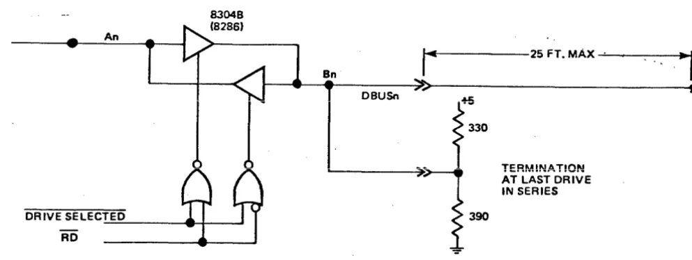
An
a. +DBUS 0-7
A high active 8-bit wide bus used to transfer commands and status between drive and controller. These lines connect directly to an 8304B (or 8286) bus transceiver as shown in Figure 2.
If long cables are used, these lines should be terminated at each end.
83048
I
~82861
1
!
25 FT. MAxBn
<1
T
08USn -~1
r
__
f~o
TERM !NA T!ONAT LAST DRIVE IN SERIES
~
9
~l
[image:22.615.63.560.468.655.2]SYMBOL
VOL VOR IOFF
V1L VIR
TABLE 11. DBUS DC CHARACTERISTICS
PARAMETER MIN MAX UNITS TEST CONDITIONS
Output Low Level 0.5 V IOL = 32 MA
Output High Level 2.4 V lOR = -5 MA
Output Off Current -0.2 mA VOFF = 0.45 V
50 mA VOFF = 5.25 V
Input Low Level 0 .. 9 V
Input High Level 2.0 V
b. + ADO-l
A high active 2-bit wide address bus, whose function is to select one of three registers in which data is stored or from which it is read. These lines connect directly to a 74LS244 Schmitt-Triggered Receiver enabled by DRIVE SELECTED as shown in Figure 3.
These lines should be terminated at the drive end. PRIAM provides an optional terminator.
1
~4'---25FTMAX---____ ~·~1
r::::--74L_S244.
---->~>~---~, I"'~
-~~T
:J:~~~---_~~----~I
1
+5VDC·
-::.- TERMINATOR
DRIVE SELECTED
[image:23.613.55.558.65.666.2] [image:23.613.53.564.405.656.2]TABLE 12. SINGLE LINE RECEIVER GATED BY DRIVE SELECT DC CHARACTERISTICS
SYMBOL PARAMETER MIN MAX UNITS TEST CONDITIONS
VIH
t1
YIL IIH
IlL
Input High Level 2 V
Input Low Level 0.8 t1 Y
High Level Input
Current 0.02 mA VI
=
2.7VLow Level Input
Current -0.2 mA VI
=
0.4Vc. - RD
This low active signal is used to gate the contents of the selected register (decode of AD1,ADO) onto the DBUS. This line is connected to a 74LS244 as shown in Figure 3. Also, the DC characteristics are listed in Table 12.
Cables should be terminated at the drive end. PRIAM provides an optional terminator as shown in Figure 3.
d. - WR
This low active signal is used to gate the contents of the DBUS into the selected register. This line is connected to a 74LS244 as sho~~ in Figure 3 and its DC characteristics are listed in Table 12.
Cables should be terminated at the drive end. PRIAM provides an optional terminator as shown in Figure 3.
e. - RESET
This low active signal resets the drive logic. If the drive is Sequenced Down when RESET occurs it will remain sequenced dowu. If the drive is Sequenced Up, the operation 13
terminated and the drive becomes Sequenced Down. This line is connected to a 74LS244 as shown in Figure 3 and its DC characteristics are listed in Table 12.
Cables should be terminated at the drive as shown in Figure
f. - DRIVE SELECT 1-4
14
»
SYMBOL
These low active signals enable drive response. No reading, writing, register selection, or command response will occur unless the drive is selected. These single-ended receiver lines are shown in Figure 4. Cables should be terminated as shown in Figure 4.
Long cable connections should be terminated at the drive. See Figure 4.
25 FT MAX
.J
)
220
+S
330
-:::: TERMINATOR
Figure 4. Single End Line Receiver
TABLE 13. SINGLE LINE RECEIVER DC CHARACTERISTICS
PARAMETER MIN MAX UNITS TEST CONDITIONS
Positive-going
threshold 1.4 1.9 V
Negative-going
threshold 0.5 1 V
High level input
current .020 rnA VI = 2.7V
Low level input
[image:25.613.67.551.259.678.2] [image:25.613.88.528.550.708.2]g. -HEAD SELECT 1-2
These low active signals are used to select the desired head for reading or writing. The head selection decoding is shown in Table 9. These lines are connected to a 74LS14 as shown in Figure 4 and its DC characteristics are listed in Table 13.
Cable connections should be terminated as shown in Figure 3. h. -READY
This low active signal from the drive indicates that it is up to speed and ready to read, write or seek. It is driven by a 75462 open collector driver as shown in Figure 5.
This line must be terminated at the controller.
. 75462
220n
"'r--
I - - -25 FT MAX - - - 1 . . 1I00I1
---~»---)~>---~---330n
DRIVE SELECTED _
Figure 5. Single Line Driver
TABLE 14. SINGLE LINE DRIVER DC CHARACTERISTICS
SYMBOL PARAMETER MIN MAX UNITS '!'.t,;ST CONDITIONS
IOH High level output
current 0.10 rnA
[image:26.615.69.559.247.671.2]_I.
t-_'
i. -INDEX
This low active signal indicates the beginning of a track. The INDEX pulse is 1.9 microseconds wide. !L is ar1ven by a 75462 open collector driver as shown in Figure 5 and has the DC characteristics listed in Table 14. This line must be terminated at the controller.
j. -SECTOR MARK
This low active signal indicates the beginning of a sector. The SECTOR MARK pulse is 960 nanoseconds wide. It is driven
by a 75462 open collector driver as shown in Figure 5 and has the DC characteristics listed in Table 14. This line must be terminated at the controller.
k. -WRITE GATE
This low active signal enables the writing of data by the selected head. This signal is received by a 74LS244 as shown in Figure 3 and its DC characteristics are listed in Table 12. Cable connections should be terminated at the drive as shown in Figure 3.
1. - READ GATE
This low active signal initiates synchronization of the drive's phase lock loop for data separation. READ GATE must be enabled during a gap. This signal is received by a
74LS244 as shown in Figure 3 and its DC characteristics are listed in Table 12. Long cable connections should be
terminated at the drive as shown in Figure 3.
m. +, - WRITE DATA
WRITE DATA is an NRZ serial data signal synchronous with WRITE CLOCK. It is received by a 75116 type differential line receiver section as shown in Figure 6.
The DC characteristics are listed in Table 15. The last drive in a string should be terminated. PRIAM offers an optional terminator.
/--7~ fT UA.X
1
---
>
>
1[AMINA10A
-,..~
TABLE 15. DIFFERENTIAL LINE RECEIVER DC CHARACTERISTICS
I
I
I
I SYMBOL PARAMETER MIN MAX UNITS TEST CONDITlooSI
VTH Differential inputhigh-threshold 0.2 V
VICR Common-mode input +15 to
range -15 V
II (REC) Receiver input
current 2.3 rnA
n. +, - WRITE CLOCK
SYMBOL
VOH
VOL
IOZ
IOH
IOL
lOS
This square wave signal from the controller is phase locked to the WRITE DATA. It must be stable from 120 nanoseconds before WRITE GATE and remain stable during WRITE GATE. The nominal period of WRITE CLOCK is 139 nanoseconds. It is received by a 75116 type differential line receiver as shown in Table 15 and Figure 6. These lines should be terminated by the optional terminator.
TABLE 16. DIFFERENTIAL LINE DRIVER DC CHARACTERISTICS
PARA~1ETER MIN MAX UNITS TEST CONDITI CNS
I
High level output
voltage 2.5 V IOH = -20mA
Low level output
voltage 0.32 V IOL = 20mA
Off-state (non-selected) output
current +0.02 rnA
High-level output
current -20 rnA
Low-level output
current 20 rnA
Short circuit output
[image:28.612.78.502.400.626.2]o. +, - READ/ REFE RENCE CLOCK
This square wave signal provides clocking and synchronization for reading and writing data~ It is derived from either the crystal oscillator or the VFO synchronized to READ DATA. The nominal period is 139 nanoseconds. It is driven by a 75113 type differential line driver as shown in Figure 6 and its DC
characteristics are listed in Table 16.
p. +, - READ DATA
This serial NRZ signal is used to transmit data from the drive to the controller. This output is valid 8 microseconds after READ GATE is enabled. It is driven by a 75113 type differential line driver as shown in Figure 6 and its DC characteristics are listed in Table 16.
In the following section, timing requirements are discussed. Register load timing is shown in Figure 7 and the AC characteristics are listed in Table 17.
AOCH
1
r
:'
~NESE~---'r~4---~----~~ ~
oeus
WR
tAW
.,
t
tow
.. I
---~~---tw--O~:~---L
~t4---t'iNW-
tRY-~J
Figure 7. Register Load Timing
TABLE 17. REGISTER LOAD AC CHARACTERISTICS
SYMBOL
tAW
~A
tww
tDWtwo
tRV
PARAMETER MIN
Address stable before WR 60
Address hold time for WR 30
WR pulse width 100
Data set up time for WR 60
Data hold time for WR 30 Recovery time between WR 200
MAX UNITS
I
[image:29.615.49.555.285.667.2]Register read timing is shown in Figure 8 and the AC characteristics are listed in Table 18.
~~~~SELECT~~
_________________________________________________-,XL ______________ _
L...=_~~
_ _ _ _ t Ae - - - -_ _ _ _ _ -!b"""'!'s..-
tRA==:J
---~---~-n---~'~~tRR~l~----·'-·~----·-·---RD
Deus
-1
:RO
J-
J
tOF
r-Figure 8. Register Read Timing
TABLE 18. REGISTER READ AC CHARACTERISTICS
SYMBOL PARAMETER MIN MAX UNITS
I
tAR Address stable before RD 60 ns tRA Address hold time for RD 30 ns
tRR RD pulse width 100 ns
tRD Data delay from RD 60 ns
tDF RD to data floating 10 40 ns
RESET timing is shown in Figure 9 and the AC characteristics are listed in Table 19.
DRIVE SELECT
[image:30.617.45.560.83.581.2] [image:30.617.64.542.532.645.2]TABLE 19. RESET AC CHARACTERI STICS
SYMBOL PARAMETER
Reset pulse width DRIVE SELECT to RESET
MIN
100
o
MAX
i
i
UNITS
I
ms II
ns
I
INDEX and SECTOR MARK timing are shown in Figure 10 and their AC characteristics are listed in Table 20.
INDEX
1 - 4 - - - tlR
SECTOR MARK
Figure 10. INDEX and SECTOR MARK Timing
TABLE 20. INDEX AND SECTOR MARK AC CHARACTERISTICS
SYMBOL PARAMETER MIN TYP MAX UNITS
tIW INDEX pulse width 1.6 1.9 2.2 us
tIR INDEX period 16.5 16.8 17.2 ms
tsw
SECTOR MARK pulse width 816 960 1100 ns tIS INDEX to first SECTORMARK 179 187 195 us
tSR* Sector width
for 44 sectors 366 374 382 us
for 32 sectors 733 748 764 us
[image:31.613.108.475.75.159.2] [image:31.613.65.556.234.377.2] [image:31.613.84.486.456.635.2]WRITE DATA and WRITE CLOCK timing relationship is shown in Figure 11 and their AC characteristics are listed in Table 21.
DRIVE SELECTED HEAD SELECT 1·2
READY
WRITE GATE
WRITE CLOCK
WRITE DATA
Figure 11. WRITE DATA ana WRITE CLOCK Timing
TABLE 21. WRITE DATA AND WRITE CLOCK AC CHARACTER! STICS
SYMBOL PARAMETER MIN TYP MAX
UNITiJ
tCLK WRITE CLOCK period 137 139 141 ns
tWH WRITE CLOCK high pulse
width 59 69.5 80 ns
tWL WRITE CLOCK low pulse
[image:32.613.56.543.117.533.2]READ DATA and READ CLOCK timing relationship is shown in Figure 12 and their AC characteristics are listed in Table 22.
DRIVE SELECT . HEAD SELECT 1-2
READ GATE
READ CLOCK
'DC tCD
r
~r
.\
I
READ DATA
0 0 1 0 1
Figure 12. READ DATA and READ CLOCK Timing
TABLE 22. READ DATA AND READ CLOCK AC CHARACTERISTICS
SYMBOL PARAMETER MIN TYP MAX UNITS
tCLK READ CLOCK period 129 139 149 ns
tWH READ CLOCK high pulse
T.~':A .. h
59 69.5 80 ns
" "" ... LI
tWL READ CLOCK low pulse
width 59 69.5 80 ns
tBIT READ DATA bit period 129 139 149 ns
\
[image:33.617.60.572.80.348.2] [image:33.617.76.459.507.642.2]Figure 13 shows timing requirements for writing full sectors (ID and data fields) and also for writing sector data fields only.
2 BYTES MIN
I
23 BYTES MIN111
BYTES MINI I
DATA FORMAT
~~~~~~=Xr----Z-E-R-O-S---~--ID--~i-x
ZEROS DATAI~
DRIVE SELECTED
~4~4---t-S-H---HEAD SELECTED _ r ' H W
~---READY
SECTOR MARK
WRITE GATE
r?
FULLSECTOR
14 tIDG---I.~1 WRITE
_ I
----LLLL...~UL.L.L.L.F f--r~-=--=-~~~L-)
(~
DATAtDF~ FIELD
r-'oG~
WRITEI f / / / / L / / / / / / / / / / / / A ' .
U
~[tSG
WRITE GATE
WRITE DATA
WRITE DATA
[image:34.617.59.571.88.562.2]TABLE 23. RECORD WRITING CONTROL AC CHARACTERISTICS
I
SYI-FlBOL PARAIvIETER ['lIN TYP IvIAX
_______ J
UNiTb i
tSH DRIVE SELECTED to HEAD
I
SELEC!IED 20 us I
I
tSR DRIVE SELECTED to READY 100 ns
tSG SECTOR MARK TO WRITE GATE -1
a
1 us t IlX; ID gap timing (23 bytes min) 18.8 22.1 ustIDF ID fill (2 Byte min) 1.63 1.92 us
tOG Data gap (no WRITE to
READ transitions (11 byte min) 8.98 10.56 us
tDF Data fill (2 Byte min) 1.63 1.92 us
tHW Head Select to WRITE GATE 100 ns
Figure 14 shows timing requirements for reading ID and data fields and for reading data fields only.
I
23 BYTES MIN 11 BYTES MINDATA FORMAT iD ZEROS DATA
OR IV E SE LECTED
HEAD SELECTED
READY
SECTOR MARK
READ GATE
I XL...-..-_
\
r
-V
READ DATA
"I~
[image:35.612.83.501.62.260.2] [image:35.612.59.571.309.664.2]TABLE 24. RECORD READING CONTROL AC CHARACTERI STIes
SYMBOL PARAMETER MIN MAX UNITS
I
tSH DRIVE SELECTED to HEAD
I
SELECTED 20 us
tSR DRIVE SELECTED to READY 100 ns
tRDLW READ GATE DELAY for gaps allowing WRITE to READ
transitions 10 us
tRDLR READ GATE DELAY for gaps limited to READ to READ or READ to WRITE
transitions 1 us
t SYN READ PLO SYNCHRONIZATION (Data not valid for this
period) 8 us
tHR HEAD SELECT to READ GATE 10 us
[image:36.615.100.464.83.320.2]25 Bytes (min.)
I
I
23 Bytes (min.)I
1t
Bytes (~in.)I
I
I
"
Bytes (min.)I
2 Bytes 2 Bytes 9 Bytes (min.) (min.)
I
(min.J 2 Byte "4 BytesI
9 Bytes(min.) (min.J (min.)
~---,-~~
DATA ZEROS . 10 INFORMATION ZEROS DATA
,
ISHORT GAP MAY BE USED IF ONLY READ . TO WRITE TRANSITIONS OCCUR.
SECTOR MARK READING BOTH ID & DATA
____________
~n~________________________________________________________________
~,"
READ GATE READ CLOCK
READ DATA
WRITING BOTH 10 & DATA WRITE GATE
WRITE CLOCK
WRITE DATA READING, 10
< WRITING DATA
t:;:/:.Lr:/·\t:::iMf?) ,::::. :.·:1
REA 0 GATE 8~0i;~i;{t~;ii:~;;Ii:;i.i~ir't~:~~j~:~!.·:::;]:i:;::;2:1
READ CLOC K Itqf:iif::ii::glf:it~it:::i~i:;;ii!#i:ii!@::i::ttt
READ DATA Ij:i:t§1t;iWi~t:j~:~miI:;rmi:tyit WRITE CLOCK
LJ
INVALID INVALID _
k-Spsec+f Valid
INVALID Valid
,
,.
Valid cont.inuously whenever the drive is ready.
t " " ' > y « r £ r £ < r « < r r r < , « « < r < , r , « « < o
INVALID Valid
,
,
INVALID Valid
,
"
r---~
Gap of Zeros , . , r
WRITE DATA l@iiitJii@Jftki~tlw~;~i'Jlfil ~
[image:37.612.40.575.120.646.2]V. SUGGESTED DATA FORMAT
A. Format Definitions
The suggested format is similar to the soft sectored format used on flexible discs.
This format has the sector ID field and the data field separated by a gap. This allows reading of the ID field to verify position, and subsequently switching to write mode during the gap and writing a new data field.
The soft sector format is shown in Figure 16 and is described below.
Each track starts with an INDEX pulse, which corresponds to a certain area of the index ring. Also, the index ring provides rotational position information for the generation of SECTOR MARK pulses. A sector pulse precedes each record and successive records are separated by gaps within which the sector pulses occur.
1. PRE-RECORD GAP (GAP 1)
The Pre-Record Gap, or Gap 1, appears at the beginning of every record. It consists of 23 bytes of zeros. The length of Gap I never varies. The first Gap 1 after INDEX is followed by the Skip Defect Record. All other Gap lis, after SECTOR MARKS, are followed by ID records.
2. SKIP DEFECT RECORD
The Skip Defect Record consists of 11 bytes: a Data Sync using the hexadecimal pattern FB, the physical address of the first defect using two bytes, the physical address of the second
defect using two bytes, the physical address of the third defect using two bytes, a check sum across the previous six bytes using two bytes, and fill characters of zeros using two bytes.
3. ID FIELD
This Identification Field uses nine bytes: an ID sync of one byte, the head address and high order cylinder address of one byte, the low order cylinder address of one byte, the sector number of one byte, a sector length and flag bytes, two CRC
Data Field Length ( bytes)
256 512 1024
5. DATA FIELD
Following Gap 2, the Data Field may consist of any number of bytes but lengths of 261, 517, or 1029 bytes are co"W~n for 256, 512 or 1024 data lengths. The first byte is a data sync, while the last four bytes consist of two bytes of CRe and two bytes of zeros for filling.
6. PRE-INDEX GAP (GAP 3)
The Pre-Index Gap, or Gap 3, is used only once on a track. It appears at the end of the last data field and persists until INDEX. This gap contains zeros.
Table 25 lists a few of the various available soft sector track formats.
TABLE 25. HARD SECTOR FORMAT INFORMATION
Sector Sectors Gap Gap Gap Data Per Data Percent
Length Per 1 2 3 Track Capacity
Utili-Track zation
(bytes) (bytes) ( bytes) (bytes) (bytes) (bytes)
304 44 23 11 28 11,264 8,560,640 75.1%
560 22 23 11 524 11,264 8,560,640 75.1%
J-i
Skip Data
Da~
Fie!d G:p Gap Defect Gap Gap Fieid Cap Gap
N
I
31
'
I
R~o,d
I '
1
101I
2I
1-I'
/1D21
2-I
INDEX 1ST SECTOR· 2ND SECTOR
MARK MARK
Gap 1: Zeros 23 Bytes
Skip Defect
Record: Data sync X'FB 1 Byte
1st defect address 2 Bytes 2nd defect address 2 Bytes 3rd defect address 2 Bytes
Check sum 2 Bytes
Fill characters - zeros 2 Bytes
Sector Mark: Derived from INDEX and servo clock
Gap 1: Zeros 23 Bytes
ID Field: ID sync 1 Byte
Head and high order cylinder
address 1 Byte
Low order cylinder address 1 Byte
Sector address 1 Byte
Sector length & flag 1 Byte
CRe 2 Bytes
Fill characters - zeros 2 Bytes
Gap 2: Zeros 11 Bytes
Data Field Data sync 1 Byte
Data n Bytes
eRe ~
Bytes
~
Fill characters - zeros 2 Bytes
Gap 3: Zeros Size depends on data field
Dau
Fieid Gap
I
I
I \
JRD SECTOR
MARK
[image:40.617.60.546.59.568.2]