IMC Growth and Shear Strength of Sn-Ag-Bi-In/Au/Ni/Cu BGA
Joints During Aging
Jeong-Won Yoon
*1, Sang-Won Kim
*1and Seung-Boo Jung
*2Department of Advanced Materials Engineering, Sungkyunkwan University, 300 Chunchun-dong, Jangan-gu, Suwon 440-746, Korea
The growth kinetics of intermetallic compound (IMC) layers formed between Sn-3Ag-6Bi-2In ball-grid-array (BGA) solder and Au/Ni/ Cu substrate by solid-state isothermal aging were examined at temperatures between 343 and 443 K for 0 to 100 days. A quantitative analysis of the IMC layer thickness as a function of time and temperature was performed. The intermetallic layer exhibited a parabolic growth at the given temperature range. Because the values of the time exponent (n) are approximately 0.5, the layer growth of the IMC was primarily controlled by diffusion over the temperature range studied. The apparent activation energy value calculated for the Sn-Ag-Bi-In/Au/Ni/Cu BGA joint was 64.8 kJ/mol. Also, the reliability of the solder ball attachment was characterized by mechanical ball shear tests. The brittleness of the solder joints increased with increasing aging temperature and time, and the fracture occurred within the IMCs and Ni layer. The deterioration of the solder ball shear strength was found to be predominantly caused by the formation of the IMC layer.
(Received September 24, 2003; Accepted January 20, 2004)
Keywords: tin-3silver-6bismuth-2indium solder, ball shear test, growth kinetics, isothermal aging, intermetallic compound
1. Introduction
The realization of harmful effects of Pb on the environ-ment and human health, coupled with the threat of legis-lation, has instigated a search for electronic packaging applications using Pbfree solders.1–4) Many different solder alloys have been proposed as potential Pb-free solder replacements and the most promising of these fall into the general alloy families of Sn-Cu, Sn-Ag and Sn-Ag-Cu.5–10)It has satisfactory wettability, reliability, ductility and strength compared to other Pb-free solders. However, even with these advantages, these alloys have a high melting point. This property can cause some problems such as thermal damage of electronic components due to the high soldering temperature and modification of the soldering equipment.11)In order to
overcome the high melting point of Pb-free solders, a Sn-Ag-Bi-In solder alloy has been suggested.11,12) This solder
material has a relatively low melting temperature (458– 488 K) compared to the Sn-Cu and Sn-Ag solder alloys.
One of the major concerns of BGA technology is the solder joint reliability.2,13,14) An electronic package is generally subjected to different thermal and mechanical loads during manufacturing, storage, transport and operation. High am-bient temperatures on the solder joint, for instance, result in the growth of unwanted intermetallic compounds (IMC), which weaken the solder joint strength because of their brittleness and weakness. Therefore, it is necessary to understand and control the factors that govern the kinetics of interfacial reaction.
The Ni coating is commonly used as a protective layer on a Cu conductor in electronic devices.14,15)It has interfaces with
the Cu substrate and with the solder. However, there is no chemical reaction at the Cu/Ni interface and the IMC layer is not expected to form at this interface because the Cu-Ni binary system only forms a complete solid solution. There-fore, the existence of this interface is not detrimental to the
solder joint.
Some studies on Sn-Ag-Bi-In solder alloy are available in the literature,11,16)but the knowledge of interfacial reaction
kinetics and ball shear tests of the solder on Au/Ni metallized Cu substrate is insufficient. Therefore, this study focuses on the growth kinetics of Ni3Sn4 IMC for Sn-3Ag-6Bi-2In
solder/Au/Ni metallized Cu BGA substrate system during solid state aging. The growth rate constants of Ni3Sn4
intermetallic were measured as a function of time and temperature, and the activation energies for intermetallic growth were calculated by the Arrhenius equation. In addition, the shear strength of the solder joints was tested as a function of the time and temperature for isothermal aging. The correlation between the shear strength and their corresponding interfacial microstructure on the solder joints are also discussed.
2. Experimental Procedures
2.1 Solder ball attachment
BGA solder used in this study was Sn-3Ag-6Bi-2In (mass%). The size of the solder ball was 500mm. The substrate was a BT (Bismaleimide Triazine) laminate with subsurface solder bond pads whose nominal size and shape were defined through a circular opening of 460mmdiameter. The pads were composed of electroplated Au/Ni over an underlying Cu pad in thickness of 0.5 and 7.0mm, respec-tively. The Sn-Ag-Bi-In solder ball was bonded to the BT substrate in a reflow process employing RMA flux in an IR 4 zone reflow machine (RF-430-N2, Japan Pulse Laboratory Ltd. Co.) with maximum temperatures of 528 K for 60 seconds, respectively.
2.2 Aging treatment and microstructural analysis
Solder joints were cross-sectioned for examination imme-diately after undergoing the reflow, as well as the aging process, in an oven at temperatures 343, 373, 393, 423 and 443 K for times ranging from 1 to 100 days, respectively. Isothermal aging of solder joints were performed in an oven
*1Graduate Student, Sungkyunkwan University
*2Corresponding author, E-mail: [email protected]
with a temperature stability of1K. The microstructural and chemical analyses of the samples were obtained by using Philips XL 40 FEG scanning electron microscopy (SEM) equipped with energydispersive X-ray analysis (EDX). The phases at the interface were identified using X-ray diffraction (XRD) analysis. In all the cases, the quantitative measure-ments of the IMC layer thickness were done using micro-graphs taken on the cross-sections of the intermetallic layer. The layer thickness was evaluated using image analysis software to measure the total area of intermetallic layer. The phase areas were divided by the length of boundary shown in the cross-section to yield the average layer thickness.
2.3 Shear strength
The shear test was performed on reflowed and aged samples by using the shear tester (Rhesca Co. Ltd., PTR-1000). The shear tool height of 50mm and shear speed of 200mm/s were used. A total of 20 solder ball joints were
sheared for each condition. After the ball shear test, the fracture surfaces were investigated thoroughly by SEM in back-scattered electron mode, as well as by EDX.
3. Results and Discussion
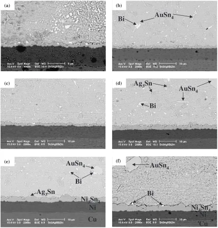
Figure 1 shows the SEM micrographs of IMC layers for the interface between Sn-Ag-Bi-In solder and Au/Ni/Cu sub-strate aged at 423 K for different aging times. During reflow soldering, the topmost Au layer dissolved into the molten solder and formed the randomly distributed AuSn4
com-pound within the solder, leaving the Ni layer exposed to the molten solder. The reaction between Ni and molten solder resulted in the formation of a Ni3Sn4layer at the interface. In
the as-reflowed joint, the thickness of the IMC was approximately 0.76mm. According to EDX analysis, the IMC formed on the BGA substrate is composed of Ni-Sn. Ag, Bi and In are not detected in the interfacial layer, indicating
(a)
(c)
Ag
3Sn
AuSn
4Ni
Ni
3Sn
4Cu
Bi
(e)
Bi
Ni
Ni
3Sn
4AuSn
4Cu
(f) (b)
Bi
AuSn
4(d)
Bi
AuSn
4Ag
3Sn
[image:2.595.84.512.72.520.2]that these elements were not directly involved in the interfacial reactions. The Ni3Sn4 IMC thickness increased
with aging time, reaching only 3.29mmfor 100 days of aging at 423 K. Furthermore, AuSn4 and Ag3Sn particles were
found within the solder material. However, reprecipitation of Au as (Au,Ni)Sn4 at the interface, as shown in the eutectic
Sn-Pb solder system,13)was not observed.
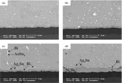
Figure 2 shows the SEM micrographs of reaction couples after 50 days aging at different aging temperatures. The aged solder joint consisted of the Ni/Cu substrate, the Ni3Sn4IMC
layer, Ag3Sn particles embedded within the Ni3Sn4 layer,
Ag3Sn particles in the solder, Bi phases, and acicular AuSn4
phases (Fig. 2(c)). With increased aging time and
temper-ature, the Ag3Sn particles became more prevalent in the
Ni3Sn4 IMC layer. This observation is consistent with a
previous study of IMC growth in a Sn-Ag based solder/ substrate diffusion couples.17,18) Also, this is in agreement
with the suggestion that Sn diffuses into the IMC layer to react with the Cu substrate. As shown in Figs. 1 and 2, as the aging conditions became more severe, the IMC layer grew.
Figure 3(a) shows the top view of Ni3Sn4 IMC after the
sample was aged for 100 days at 343 K. The specimen (coupon type) for XRD analysis was prepared by mechan-ically removing the solder and etching away the remaining solder part. The IMC found at the interface exhibited a facet structure, and the size of the IMC phase was about 1–3mm.
(a) (b)
(c)
Bi
Ag
3Sn
Ni
3Sn
4AuSn
4Bi
(d)Bi
Ni
Ni
3Sn
4Cu
Ag
3Sn
Fig. 2 SEM micrographs of a Sn-3Ag-6Bi-2In/Au/Ni/Cu interface after aging for 50 days at; (a) 343 K, (b) 373 K, (c) 393 K and (d) 443 K.
(b)
20 30 40 50 60 70 80
Ag
3Sn
Cu Ni3Sn4
Intensity (arb. unit)
Diffraction Angle, 2θ
(a)
5
µ
m
[image:3.595.85.511.73.364.2] [image:3.595.86.515.420.585.2]The Ni3Sn4intermetallic surface shown in Fig. 3(a) was then
used to obtain the X-ray diffraction pattern of the IMC, shown in Fig. 3(b).
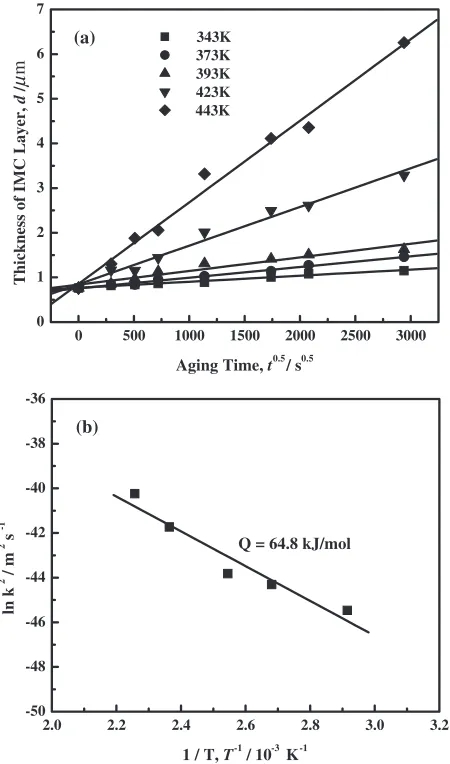
The curve of the average thickness of the Ni3Sn4 IMC
versus the square root of aging time at different aging temperatures is given in Fig. 4(a). All the data points fitted well with the following classical theory of diffusion;
W ¼ktn ð1Þ
whereW is the thickness of the IMC layer,kis the growth rate constant,tis the reaction time andnis the time exponent. The IMC layer thickness was found to increase linearly with the square root of aging time and the growth was faster for higher aging temperatures.
The growth rate constant was calculated from a linear regression analysis of W versus t0:5, where the slope = k.
Table 1 lists the growth rate constants calculated for the Ni3Sn4IMC layer at different aging temperatures. All of the
linear correlation coefficient values (R2) for these plots were greater than 0.97. This good linear correlation suggests that the growth of the IMC layer is controlled by diffusion over the temperature range studied. As mentioned above, the growth rate of IMC was faster for higher aging temperature.
If the growth process was controlled by diffusion, the increase of the IMC layer after aging should follow the square root time law,W ¼kt0:5. It is empirically found that the time exponent (n) takes the value of 0.5 when the diffusion reaction is controlled by volume diffusion.19)The
time exponent was evaluated from the equation of the growth kinetics at each aging temperature (Table 1). The diffusion processes appeared to be largely responsible for growth of the IMC layer, although the time exponents were not exactly 0.5. The following simple Arrhenius relationship was used to determine the activation energy for the Ni3Sn4IMC growth
respectively;
k2¼k02expðQ=RTÞ ð2Þ
wherek2 is the square of growth rate constant (m2/s),k02is
the frequency factor,Qis the activation energy,Ris the gas constant (8.314 J/mol-K) and T is the aging temperature (absolute units). The activation energies were calculated from the slope of the Arrhenius plot using a linear regression model. Figure 4(b) shows the Arrhenius plot for the growth of the Ni3Sn4 IMC layers. The apparent activation energy
calculated for the growth of the Ni3Sn4 intermetallic was
[image:4.595.57.282.74.456.2]64.8 kJ/mol.
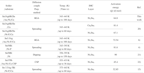
Table 2 lists the values of the activation energy (Q) obtained from the temperature dependence of k2, with the
data from previous works.4,6,15,20–22) Although some
differ-ence does occur in the data, our result is in good agreement with the results of these previous workers. The discrepancy among the activation energies is due to the differences in the solder alloy,23,24) surface finish of substrates4,20) and aging temperature range.18)
Ball shear strength values were measured to evaluate the effect of the interfacial IMC reactions on the mechanical reliability of solder balls as a function of aging conditions. Figure 5 shows the variation of shear strength of the solder balls with respect to aging temperature and time. The average shear strength of the solder joints after reflow was about 14.8 N. As a whole, the shear strength decreased with increasing aging temperature and time. As shown in Fig. 5, it can be clearly seen that initial aging increased the shear strength of solder joint. We also reported a similar result in our previous work.2)Compared to the IMC thickness data of
Fig. 4(a), the IMC thickness has a strong influence on the solder ball shear strength. Increasing the storage temperature and the dwell time leads to increasing the thickness of IMC layers. On the other hand, the ball shear strength was observed to decrease with increasing thickness of the IMC layers. During aging at temperatures of 343, 373 and 393 K, there is relatively little change in the shear strength with
Table 1 Calculated the square of growth rate constants (k2), linear correlation coefficients (R2) and time exponents (n).
IMC Temp. R2 k
2
n
(K) (1019m2/s)
343 0.99 0.18 0.44
373 0.99 0.57 0.53
Ni3Sn4 393 0.97 0.93 0.47
423 0.99 7.50 0.45
443 0.99 33.48 0.49
0 500 1000 1500 2000 2500 3000
0 1 2 3 4 5 6 7
Thickness of IMC Layer,
d
/
µ
Aging Time, t0.5 / s0.5 343K
373K 393K 423K 443K
2.0 2.2 2.4 2.6 2.8 3.0 3.2
-50 -48 -46 -44 -42 -40 -38 -36
Q = 64.8 kJ/mol
ln k
2 / m 2 s
-1
1 / T, T-1 / 10-3 K-1 (b)
(a)
m
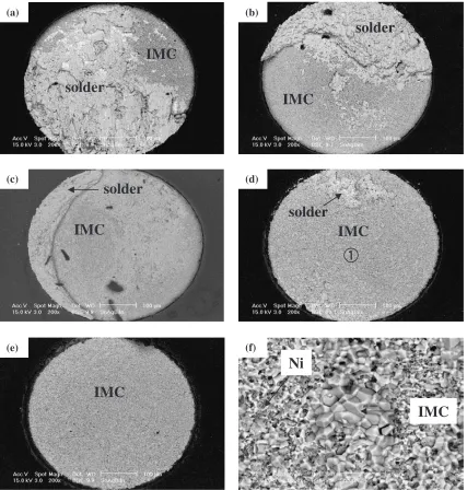
[image:4.595.304.548.94.183.2]aging time. However, in the case of 423 and 443 K, the shear strength decreased sharply with increasing time. From the shear test result, the shear strengths decreased by 1, 3, 4, 18 and 29% after aging for 100 days at temperatures of 343, 373, 393, 423 and 443 K compared to the strength measured after reflow, respectively. To verify the variation of shear strength, the fracture surfaces were examined by the SEM. After isothermal aging, the fracture surface showed various characteristics depending on aging temperature and time. Figure 6 represents the fracture surfaces after aging for 100 days at various aging temperatures. In the case of as-reflowed sample (Fig. 6(a)), the fracture surface shows ductile and slightly brittle failure. The brittleness of the solder joints increased with increasing aging temperature and time, and
the fracture occurred within the IMCs and Ni layer (Fig. 6(f)). According to EDX analysis, the fracture occurred at the interface between the solder and Ni3Sn4 IMC layer and/or
Ni3Sn4IMC layer and Ni layer. As shown in Fig. 6(e), more
severe aging resulted in a flat-fracture surface and solder alloy was not present on the fracture surface. From these fractographs, it is clear that these interfaces fail in a very brittle mode. In the ball shear test, fracture occurs at the interface or in the region with the lowest strength. In this study, a fracture analysis indicated that the shear strength could be related to the roughness of the IMC interface. After significant aging, the IMC layer grew and the interface between the IMC layer and bulk solder became smooth (Fig. 1 and 2). Therefore, an adhesive strength came mostly from the bonding strength of the IMC/solder interface. Consequently, IMC thickness and thermal loading history significantly affect the integrity of solder balls in BGA packages.
4. Conclusion
The effects of isothermal aging (343-443 K) on the IMC growth and ball shear strength of Sn-3Ag-6Bi-2In solder/ Au/Ni/Cu BGA substrate were presented in this paper. The following conclusions were obtained:
(1) During reflow soldering, the topmost Au layer dissolved into the molten solder and formed the randomly distributed AuSn4 compound within the solder, leaving the
Ni layer exposed to the molten solder. The reaction between Ni and molten solder resulted in the formation of a Ni3Sn4
layer at the interface. Ag, Bi and In are not detected in the interfacial layer, indicating that these elements are not directly involved in the interfacial reactions.
[image:5.595.50.551.84.340.2](2) The IMC layer thickness was found to increase linearly with the square root of aging time and the growth was observed to be faster for higher aging temperatures. The
Table 2 Activation energies for the growth of IMCs together with values reported in previous works.
Diffusion
Activation
Solder couple Temp. (K) IMC
energy Ref.
/substrate Prep. /Time (s) Layer
(Q, kJ/mol) method
Sn3Ag6Bi2In
BGA 343–443 K Ni3Sn4 64.8 This
/Au/Ni/Cu /up to 100 days work
Sn3Ag8Bi5In
Cu6Sn5 81.4
/Cu
Spreading 343–443 K 20)
Sn3Ag8Bi5In /up to 60 days
Ni3Sn4 67.1
/Ni-P/Cu
Sn3.5Ag
BGA 343–443 K Ni3Sn4 72.54 6)
/Au/Ni-P/Cu /up to 100 days
Sn58Bi
Spreading 343–393 K Ni3Sn4 81.6 4)
/Ni-P /up to 60 days
Sn58Bi
Dipping 358–393 K Ni3Sn4 90 21)
/Ni /up to 150 days
Sn37Pb
CSP 353–433 K Ni3Sn4 45.4 22)
/Au/Ni/Cu CSP /up to 36 days
Sn-3.5Ag-5Bi
Spreading 373–443 K Ni3Sn4 52.85 15)
/Ni-P/Cu /up to 60 days
0 500 1000 1500 2000 2500 3000
8 10 12 14 16 18 20 22
Shear Strength ,
F
/ N
Aging Time , t0.5 / s0.5
343K 373K 393K 423K 443K
[image:5.595.55.285.370.561.2]diffusion processes appeared to be largely responsible for growth of the IMC layer, although the time exponents were not exactly 0.5. The apparent activation energy value calculated for the Sn-Ag-Bi-In/Au/Ni/Cu BGA joint was 64.8 kJ/mol.
(3) The shear strength decreased with increasing aging temperature and time. During aging at temperatures of 343, 373 and 393 K, there is relatively little change in the shear strength with aging time. However, in the case of 423 and 443 K, the shear strength decreased sharply with increasing time. The fracture occurred within the IMCs and Ni layer. The deterioration of solder ball shear strength was found to be predominantly caused by the IMC thickness and thermal loading history.
Acknowledgements
This work was supported by the Advanced Materials and
Process Research Center for IT at Sungkyunkwan University, Korea (Grant No. R12-2002-057-03001-0).
REFERENCES
1) D. R. Frear, J. W. Jang, J. K. Lin and C. Zhang: JOM53(2001) 28–32. 2) C. B. Lee, S. B. Jung, Y. E. Shin and C. C. Shur: Mater. Trans.42
(2001) 751–755.
3) K. Suganuma, K. Niihara, T. Shotoku and Y. Nakamura: J. Mater. Res. 13(1998) 2859–2865.
4) J. W. Yoon, C. B. Lee and S. B. Jung: Mater. Trans.43(2002) 1821– 1826.
5) J. Glazer: Int. Mater. Rev.40(1995) 65–93.
6) C. B. Lee, J. W. Yoon, S. J. Suh, C. W. Yang, C. C. Shur, Y. E. Shin and S. B. Jung: J. Mater. Sci. Mater. Electron.14(2003) 487–493. 7) C. H. Raeder, L. E. Felton, V. A. Tanzi and D. B. Knorr: JEM23(1994)
611–617.
8) Z. Mei and J. W. Morris, Jr.: JEM21(1992) 599–607.
9) T. Y. Lee, W. J. Choi, K. N. Tu, J. W. Jang, S. M. Kuo, J. K. Lin, D. R. Frear, K. Zeng and J. K. Kivilahti: J. Mater. Res.17(2002) 291–301.
(b)
solder
IMC
(a)
solder
IMC
(c)
solder
IMC
(d)
IMC
solder
(e)
IMC
(f)
Ni
IMC
[image:6.595.86.513.72.520.2]10) K. N. Tu, A. M. Gusak and M. Li: J. Appl. Phys.93(2003) 1335–1353. 11) M. I. Kim, J. K. Moon and J. P. Jung: Mater. Trans.43(2002) 1791–
1796.
12) C. S. Yoo, US Patent 5843371.
13) K. Y. Lee and M. Li: JEM32(2003) 906–912.
14) C. H. Zhong and S. Yi: Soldering Surf. Mount Technol.11(1999) 44– 48.
15) J. W. Yoon, C. B. Lee and S. B. Jung: JEM32(2003) 1195–1202. 16) Y. Nakahara, R. Ninomiya, J. Matsunaga and T. Takemoto: Proc. 5th
Symposium on Microjoining and Assembly Technology in Electronics, Yokohama, February 4-5, 1999, Japan Welding Society, Tokyo (1999) 341–346.
17) D. R. Flanders, E. G. Jacobs and R. F. Pinizzotto: JEM26(1997) 883– 887.
18) S. Choi, T. R. Bieler, J. P. Lucas and K. N. Subramanian: JEM28 (1999) 1209–1215.
19) J. Burke: in ‘‘The Kinetics of phase transformations in metalls’’, translated from English by K. Hirano and H. Hori (Kyoritsu, Tokyo, 1972) p. 190.
20) J. W. Yoon, C. Y. Lee, C. B. Lee, C. S. Yoo and S. B. Jung: Z. Metallkd.94(2003) 453–457.
21) C. Chen, C. E. Ho, A. H. Lin, G. L. Luo and C. R. Kao: JEM29(2000) 1200–1206.
22) P. L. Tu, Y. C. Chan, K. C. Hung and J. K. L. Lai: Scr. Mater.44(2001) 317–323.