Abstract —As the semiconductor industry market becomes more competitive, it is essential for raising semiconductor wafer yields to reduce product costs. For saving yields, many engineers have improved the many steps of wafer fabrication processes. However, stabilization in the fabrication steps is hard because there are many variations to control. We focus on the wafer probing test process to find factors of raising yields because it is not more complicate than the fabrication process to save wafer yield. Furthermore, it is more effective than the fabrication process in the aspect of the cost.
There are two kinds of failures in the wafer probing test step. One is originated from the bad quality of wafers and the other is originated from the unstable probing equipments irrelevant to the quality of wafers. Thus, it is very important to remove the second types of failure. In order to remove this type of failure, if wafers are tested as failure at the wafer probing test step, experts inspect those to determine the type of failure. If it is determined originated from the unstable equipments, the wafer will be tested once more. Since all fail wafers are inspected by human experts, the decision of retest is very time-consuming and the reliability is also very low.
In this paper, an automated wafer retesting system is proposed for raising yields in the wafer probing test. We develop an artificial neural network model to distinguish the types of wafer failures. We use the EBP (Error Back Propagation) algorithm for training the neural network. We obtain a meaningful accuracy of the failure type discrimination. The proposed system has been adopted into the mass production fields and the total wafer yields was improved by about 0.1% and the total wafer testing time was reduced by about 80%.
Index Terms—Neural network, Raising Yield, Retest, Wafer Probing Test
I. INTRODUCTION
he wafer probing test process is a test step after fabrication process. A lot consists of 25 wafers, and a wafer contains 1,000~1,500 chips. Each chip has dozens of test pads for wafer probing. The main equipments for the wafer probing test are the tester and the probe card. The tester generates many kinds of electrical signals through the pattern generators. The probe card acts as a signal bridge between the tester and the test pads on chips. Since there are many small pads on chips, the probe card has many fine needles to contact to the pads. Through the fine needles, the
Manuscript received August 11, 2011; revised August 18, 2011. This
work was supported by Samsung electronics.
Sung-in Jang is with Sungkyunkwan University, Suwon, Korea(e-mail: [email protected] ).
Jee-Hyong Lee is with Sungkyunkwan University, Suwon, Korea ( e-mail: [email protected] ).
tester sends electrical test signals to determine the quality of individual chips [1].
Usually, many errors can occur in the wafer probing step. One of major errors is sorting non-defective chips as defective ones. In order to reduce such errors, most of systems usually retest such wafers. However, all of such wafers are not retested because the cost of retest is very high. Usually, engineers look into erroneous wafers and if it seems that the wafers have problems, engineers decide to perform the retest of the wafers.
This manual retest system has many problems. First, since the human expert judge whether erroneous wafers need to be retested or not, the probability of misjudgment is high. This can cause unnecessary retesting of wafers or missing of wafers that really need to be retested. This results in a low tester efficiency and yields loss. Second, if engineers judge that a wafer needs retest, the lot including the wafer have to wait until the test of all wafers in the current lot finishes. After finishing the current lot, the lot including the wafer to be retested is reloaded and the retest of the wafer is performed. This retest process, waiting and reloading of a whole lot for retesting just one wafer, is very time-consuming, so that the performance of the tester is reduced.
Thus, the decision process of retests needs to be converted to an automated real-time process with a high accuracy. If the accuracy of automated retest system is high, the system can retest wafers which really need to be retested. If the decision process is real time, the retest time can be decreased. If a wafer fails to pass the test, the decision process can run right after without unloading the wafer. Then, the decision process instantly determines whether the wafer needs retest or not. If the wafer is determined to be retested, the test process can be done once more on the wafer. This process can remove waiting and reloading of the whole lot including erroneous wafers. Thus the testing error and the testing time can be removed. The question is how to build such automated decision process. During the wafer probing test, a lot of data on each wafer is accumulated such as fail bits, yields, bin numbers and contact resistance. The data can be used to analyze the status of wafers. Based on these data, we developed a system with a neural network which can determine whether fail wafers need retest or not.
There are also some researches using such data. Lin used the bin map data to trace root causes by using neural networks [2]. In the research, he sorted the wafer bin map pattern by pattern similarity. Chen used the map to defect patterns to analyze possible failure causes in the fabrication process by using neural networks [3]. There is little research on the automation of wafer retest in the wafer probing test. Horng applied genetic algorithms to minimize the overkills in the wafer probing test [4]. He developed an algorithm to optimize the cost of retest in the wafer probing test. They used few data for their research and did not present any
An Automated Retesting Approach
for Wafer Probing Test Systems
Using Neural Networks
Sung-In Jang, Jee-Hyong Lee
analysis on yield improvements results. The authors did not apply it to the mass production field.
In this paper, we propose an automated retest system based on neural networks. The proposed system can more accurately determine wafer retests than human experts and shows an improvement in the testing time and the overall wafer yield. We will introduce the basic theory, and propose an automated retest system. Finally, we adopt the proposed system into the mass production fields. The improvement in mass production fields will be presented.
II. BASIC THEORY
A. Neural Network
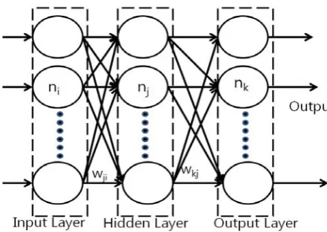
Neural networks are computational models that consist of nodes that are connected by links[5]. Each node works an operation to calculate its output value from input values. Neural networks are used for pattern mapping, pattern completion, pattern classification, etc. In medical industry, for example, neural networks are used for accurate diagnosis by visual medical images classification. The three-layer feed forward neural network is the most widely used among many neural networks architectures. The architecture of the automated retest system is the three-layer feed-forward neural network as shown in Fig. 1. The three-layer feed-forward neural networks are composed of three layers: the input layer, the hidden layer, and the output layer. The nodes in the input layer get the external input values, and the output values of the nodes transfer to the hidden layer by the links. Finally, the nodes (ni) of the hidden layer transmit the
adjusted signal by wji from input layers to the nodes (nj) in
[image:2.595.326.527.57.175.2]the output layer. This kinds of neural networks called feed-forward neural networks because the signal flow from the input layer to the output layer in a one-way direction [6].
Fig. 1. The Three-layer Feed Forward Neural Network.
The signals of each node in the layers can be adjusted by weights associated with each link. These weights can be learned from a set of training data. The well known learning algorithm is the EBP (Error Back Propagation) explained in the next section.
Fig. 2. The computation of a Neuron. The node calculates a weighted sum of all input xk .
Fig. 2 illustrates the output calculation of node nj. It
consists of two steps: the calculation of weighted summation of all input signals and the nonlinear transformation of the summation. Sj is a weighted sum of all input nodes in eq. (1). Xi is the output of node ni. and Wij is the weight between
node ni and nj.
Sj = ∑ (1)
The calculated sum is inserted to the predefined nonlinear function, f, to calculate the output signal of the node. Combining with eq. (1), we can write the output nj, Xj, as follows:
Xj = f(Sj) = ∑ (2)
B. EBP(Error Back Propagation)
The error back propagation is the most widely used algorithm for the neural network learning. The basic scheme of the algorithm is that if the neural networks give the wrong answer, the weights are corrected in accordance with error correction rules [7]. An error is the difference between the actual answer and the target answer in the neural networks. This error correction way repeats many times until the weights no longer changes. The procedures are as follows [8]:
A. Input the values of learning patterns to the nodes in the input layer, and calculate Sj with ‘Wji’, and
output Oj with Sj.
Oj = fi(Sj) (1) Sj = ∑
Wji: The weighted value between the input
and the middle layer.
Oi: The output values of the input layer. fi: The activation function of the middle layer.
B. Calculate the Ok after computing the Sk
Ok = fk(Sk) (2) Sk=∑
Wkj: The weighted value between the middle
andoutput layer.
Oj: The output value of the middle layer. Ok: The output value of the output layer. fk: The activation function of the output layer.
C. Evaluate error signal δpk from the difference between the target value tpkand the output value of neuron Opk.
δpk = (tpk - Opk)fk(Sk) (6) δpk: The variation of output layer.
[image:2.595.58.297.452.621.2]fk: The activation function of output layer.
D. Evaluate the error signal δpj connecting to neuron j from Wkjand netpj
δpj = fi(Sj) ∑ (7) δpj: The variation of the middle layer.
Wkj: The weighted value between the middle and
the output layer.
E. Adjust Wji connecting to node j of the middle layer
and node i in the input layer, and Wkj connecting to
node k of the output layer and node j in the middle layer.
Wkj(new) = Wkj(old) + α (9) Wji (new) = Wji(old) + α (10) Wkj(new):The new weight value between the
middlelayer and output layer. Wkj(old): The old weight value between the the
middle layer and the output layer. Wji(new):The new weight value between the input
layer and the middle layer.
Wji(old): The old weight value between the input
layer and the middle layer.
α: The learning rate of neural networks.
F. Repeat A to E until learning of all patterns finishes. G. Repeat A to G until the minimum square error
function E does not over the allowable error. E = ∑ ∑ (11)
III. Data Analysis for Using Input Data
A. Failure types in wafer probing test.
The wafer probing process is the last step of wafer process. There are two wafer failure types in the wafer probing test: One is originated from the bad quality of wafers and the other is originated from the unstable probing equipments irrelevant to the quality of wafers. In this step, the tester sends particular signals for wafer testing. If there are some particles on the probe card needles or the tester signal timing is not properly adjusted, non-faulty wafers can be determined as erroneous ones in the wafer probing step. The statistics shows that 73% of the retested wafers were determined non-faulty and 27% were still determined faulty. The role of an automated retesting system is detecting failure wafers which truly can be improved.
During the wafer probing test, a lot of data on tested wafers are accumulated such as fail bits, yields, bin numbers and contact resistance. If engineers analyze these data, they can determine whether a fail wafer is really defective or not. For example, the engineer can distinguish the failure wafers from the fail bits. Fig. 3 shows a failure map and a good map sorted by fail bits in the wafer probing test. In the map, the fail bits are presented by black squares. The wafer in Fig 3-(a) has a little fail bits. So, even if it was sorted as a faulty one in the test process, engineers can determine that the wafer is not really faulty by seeing the fail bit map.
(a)Good Wafer Map (b) Failure wafer map Fig. 3. Good wafer map vs. failure wafer map.
B. The candidate input data for neural networks
In this section, the data accumulated in the test process is described. The data fields are fail bits, yields, bin numbers and contact resistance.
Fail bits
Fail bits show the number of bad cells in an individual chip. The whole wafers undergo the function test in the wafer probing process. The functional test is a way of finding out whether the chips on a wafer work right or not. A wafer consists of hundreds of chips, and chips consist of millions of bits. The function test is executed on wafers by a bit unit. If there are bad bits in a chip, the number of fail bits will be recorded in the system. These data are very useful for analyzing wafers. Based on the fail bit distribution, the root causes of the failure wafers can be determined.
Bin Numbers
The bin numbers are the IDs of test items which each chip fails to pass. Each product has its own bin numbers. After the fabrication process, wafers undergo several short/open tests, and then several voltage or current tests. These bin numbers are also stored in the database. The bin numbers can be used for wafer yields analysis or package test1 information. The statics show that most of the wafers determined faulty in the retest process have problems with some particular bin numbers. However, all wafers which have problems with such particular bin numbers in the first test are not determined faulty in the retest process. Thus, the bin numbers can be used to filter out wafers before the retest process.
D/C Measure
When D/C test starts, the tester measures many voltage values and current values to find out whether a chip is good or bad by comparing standard values. D/C measuring data are the measured values of individual D/C test items. These data are also used for wafer yields analysis.
CRES (Contact Resistance)
CRES is the values of the contact resistance between probe card tips and wafer pads. The probe card works as a bridge between the tester and wafers. It sends the signal from the tester through the fine needles on the probe card [9]. However, after thousands of testing, some adherent oxide and contaminant from the aluminum pad can stack on the probe card tips. As a result, the contact resistance is unstable and becomes high. To avoid this problem, we made a
1 After the wafer probing test, the wafer is cut by sawing machine and
contact resistant limit to execute needle polishing appropriately. These data are also used for yields analysis, and it is a very important index to find the error wafers in wafer probing steps.
Yields Data
Yield data means, the percentage of good chips among the whole chips in a wafer. Most low yield wafers originate in the fabrication process problem, but there are some wafers due to unstable testing equipments. Therefore we also use these data for yield analysis in the current system.
C. Results of data analysis
In order to verify which data fields are useful for the automated retest system, we analyze the data. We collected the data for 3 months. The data are saved in the tester database. Fig. 4 shows the data in the tester database. We made a verification program in C language, and analyze the data [10].
Fig. 4. Chip data on the wafer map from database.
“F=” Fail Bits, “M=” D/C Measure, “V=” CRES. “B=” Bin Numbers
As mentioned, in the real production fields, each product has its own bin numbers. So, bin number cannot be inputs of the automated retest system which tests all kinds of products. For this reason, we exclude the bin numbers in this analysis. However, we use the bin number for wafer filtering, because we can distinguish the wafers which need the retest from ones which do not by bin numbers. Before data analysis, we filter the wafers using bin number data.
We made the simple program to find the significant data fields for the automated retest system. The program opens the wafer file and extracts the fail bits, CRES, yields, and D/C measure. The analysis program indicates the abnormal data which have the gap comparing with the average values. Finally, the engineer retests the wafer whether the wafer is failure or not.
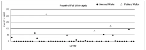
Fail bit analysis results
[image:4.595.316.568.204.285.2]Based on the data analysis program, we generate the result chart of fail bits.
Fig. 5. Results of fail bit analysis. Black triangles mean the faulty wafers. X axis: LOT ID, Y axis: Number of fail bits
We plot a graph of the number of fail bits and lot IDs. In the figure, black and white triangles represent normal and faulty wafers, respectively. Failure wafers usually have
many fail bits but normal wafers do not. Therefore after analysis, we can conclude that fail bits can be used for input data of the automated retesting system.
Contact resistance analysis results
Contact resistance means the resistance between the wafer pad and the probe card needles. If contact resistance is high, we can say that contacts between pads and tips are unstable. Fig. 6 shows the result of contact resistance data analysis result. Most of high CRES wafers are fail wafers and they need to retest. This result implies that CRES data can be used for the automation retest system.
Fig. 6. Results of CRES data analysis. Most of the high ranked triangle dots turned out the failure wafer. X axis: Lot ID, Y axis: CRES.
Yield analysis results
[image:4.595.306.557.418.512.2]Fig. 7 illustrates the result of the yields analysis. There is no significant correlation between fail wafers and yields. However, in the case of a yield of lower than 30%, such wafers are failure, so we can determine that those are faulty without the retest process. Therefore, we exclude the under the 30% yield wafers for input of auto retesting systems.
Fig. 7. Results of yield data analysis. Triangle dots are revealed to normal wafers, but under the 30% yield wafers are due to fabrication process. X axis: LOT ID, Y axis: Yields.
D/C measure analysis results
[image:4.595.306.558.608.700.2]There is D/C measure analysis results in Fig. 8. This result chart implies that D/C data cannot be input data for the automated retesting system. We cannot find a strong relation between D/D measures and fail wafers.
Fig. 8. Results of D/C Data analysis .There are no failure wafers on the high measured values. X axis: LOT ID, Y axis: Voltage.
IV. Training Result of ANN from Selected Inputs
[image:4.595.47.288.637.720.2]We use the EBP (Error Back Propagation) algorithm with 150 training data. The input data were the fail bits and CRES.
Fig. 9. Structure of artificial neural network for training
[image:5.595.314.564.145.286.2]We set up the leaning rate to 0.75 and the iteration number to 100,000 times. Fig. 10 illustrates error decreasing by EBP model. We retest wafers if the output of the neural network is larger than or equal to 0.7. This threshold is experimentally chosen.
Fig. 10. Error while training
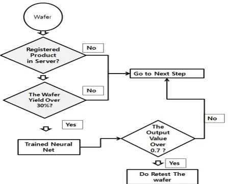
[image:5.595.54.298.357.437.2]We test the performance of the neural networks with 60 non-faulty and 15 faulty wafers. Among these wafers, 14 wafers are determined to be retested by the neural network. In the 14 wafers, 13 are faulty ones and one wafer is non-faulty. That is, the precision is 92.8% and the recall is 86.7%. Fig. 11 is the final logic of the automation retest algorithm which was installed in all of the testers in the real wafer probing step.
Fig. 11. Automated retest algorithm. Before entering the auto retesting system, the system checks whether the products are registered or not. If the wafer yields over the 30%, the wafer will enter the auto retesting system. If the output value is over 0.7, the logic executes retesting the wafer.
V. System Setup for Automated Retest System
Based on the experimental results, we set up the automated retest systems in the mass production fields. The flow chart of the automated retest systems is shown in Fig. 12.
Fig. 12. The flow chart of automated retest system. The engineer sends to the file which includes device name and yield limit. Before the wafer entering auto-retest algorithm, the algorithm filters unnecessary wafers by reading the information file
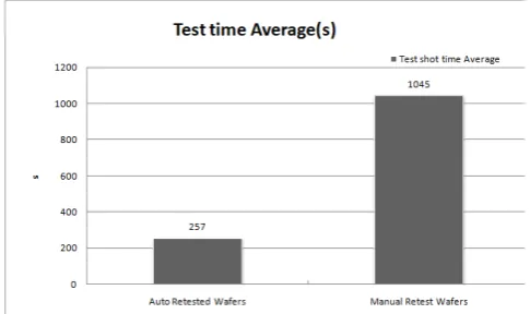
[image:5.595.313.569.539.713.2]We chose a matured product because the data of a new product are unstable so that it is not proper to apply the automated retest system. For operating the retest system process, engineers resister the major bin numbers of the product which have a strong relation to fail through the user interface server first, and then the user interface server sends the information as a file form to each tester. If a wafer which has the registered bin numbers comes, the tester sends the wafer data to the retesting algorithm. If a wafer needs retest, the tester retests the wafer and then the wafer flows to the next step. Fig. 12 is the automated retesting system in the mass production fields. We set up the automated retest system to the wafer probing testing process. There was important improvement by the automated retest system. We get 7.68% yields improvement at minimum and reduce 79.3% of the test time.
[image:5.595.56.280.555.735.2]Fig. 13. The effect of Test Time Reduction
The system save the testing time about 79.3% comparing with manual retesting wafers
Table 1 shows the actual yields improvement by the adoption of the automated retest system to the wafer probing step. We adopt the system to 12 products in the mass production fields. The total accuracy of most of product is 100%, but the Product 8 was 96.4%. The total yields improvements after adopt the automated retesting system was 34.7%. The total manual retest wafers are 13 wafers which cannot be detected by the automated retesting system. Fig. 14 illustrates the effect of test time reduction. The total test time was reduced to 79.3% comparing with manual retest wafers.
VI. Conclusions
Before the automated retest system, we cannot help testing manually. When we retest the failure wafers manually, the wafer needs to wait until the test of the current lot finishes. This point makes more time consumption than retesting directly by automated retesting system. Therefore, we adopt the automated retesting system, and get the improvements about the test time reduction and wafer yields. For making the automated retesting system, we use the neural network and extract distinct data such as contact resistance, fail bits, and yields by data analysis. We also made an environment for the retest system such as user interface.
This research results are very meaningful to companies which have wafer probing tests. An automated retesting system has more advantages than manual retesting. This system judges whether the wafers need retest or not, and executes retesting automatically. These systems reduce the wafer test time and cost in the wafer probing test. However, these systems have been adopted only in DRAM test process because DRAM memory type is nonvolatile type. This nonvolatile memory can be tested in the same process and tester, because the tested data can be erased from memory cell. However NAND FLASH memory, called nonvolatile, cannot be erased the programmed data from memory cell directly [10]. These factors are one of main limits of retesting in the same process and tester. Therefore, to build an automated retest system for NAND FLASH MEMORY, we have to invent new system flow and program. This is a future research subject for making NAND FLASH automated retest system.
Reference
[1] S.H. Kang, “Memory Test”, Seoul, Deayoungsa, 2001, pp. 85 – 101 (in Korean).
[2] F.L. Chen, S.C. Lin, Y.Y. Doong, K.L. Young, “LOGIC Product Yield Analysis by Wafer Bin Map Pattern Recognition Supervised Neural Network,” in Proceedings of the 2003 IEEE International Symposium on Semiconductor Manufacturing, San Jose, CA, 2003, pp. 501–504.
[3] F.L. Chen, S.F. Liu, “A Neural-Network Approach to Recognize Defect Spatial Pattern in Semiconductor Fabrication,” IEEE Transactions on Semiconductor Manufacturing, vol. 13, no.3, pp. 366-373, Aug. 2000.
[4] S.C. Horng, H.-T. Tsou, “Apply Genetic Algorithm to
Minimize the Overkills in Wafer Probe Testing,” in Proceedings of the 2010 IEEE international Electronics and Applications, 2010, pp. 593.
[5] M. T. Hagan, H. B. Demuth, M. H. Beale. “Neural Network Design”, Boston, MA: PWS Publishing, 1996. Pp 240-300.
[6] J. Yen, R. Langgary, “Fuzzy Logic Intelligence, Control and Information”, Prentice Hall,1998, pp. 441 – 446.
[7] J. Nilsson, Artificial Intelligence: “A New Synthesis”, Morgan Kaufmann Publishers, inc, Sanfrancisco, California, 1998, pp. 37 – 55.
[8] J.E. Dayhoff, “An Introduction Neural Network Architectures”, New York, Van Nostrand Reinhold,1990, pp.58-79
[9] J.J. Broz, R.M. Rincon, “Probe contact resistance
variations during elevated temperature wafer test,” in Proceedings of Test conference, 1999, pp.396-405. [10] R. Micheloni, L. Crippa, A. Marelli, “Inside Nand