Ames Laboratory Accepted Manuscripts
Ames Laboratory
11-12-2018
The role of Anderson’s rule in determining
electronic, optical and transport properties of
transition metal dichalcogenide heterostructures
Ke Xu
Fudan University
Yuanfeng Xu
Fudan University
Bo Peng
Fudan University
Hezhu Shao
Chinese Academy of Sciences
Gang Ni
Fudan University
See next page for additional authors
Follow this and additional works at:
https://lib.dr.iastate.edu/ameslab_manuscripts
Part of the
Biological and Chemical Physics Commons
, and the
Physical Chemistry Commons
This Article is brought to you for free and open access by the Ames Laboratory at Iowa State University Digital Repository. It has been accepted for inclusion in Ames Laboratory Accepted Manuscripts by an authorized administrator of Iowa State University Digital Repository. For more information, please [email protected].
Recommended Citation
Xu, Ke; Xu, Yuanfeng; Peng, Bo; Shao, Hezhu; Ni, Gang; Li, Jing; Yao, Mingyuan; Lu, Hongliang; Zhu, Heyuan; and Soukoulis, Costas M., "The role of Anderson’s rule in determining electronic, optical and transport properties of transition metal dichalcogenide heterostructures" (2018).Ames Laboratory Accepted Manuscripts. 307.
The role of Anderson’s rule in determining electronic, optical and transport
properties of transition metal dichalcogenide heterostructures
Abstract
Two-dimensional (2D) transition metal dichalcogenides (TMDs) MX2 (M = Mo, W; X = S, Se, Te) possess
unique properties and novel applications in optoelectronics, valleytronics and quantum computation. In this
work, we performed first-principles calculations to investigate the electronic, optical and transport properties
of the van der Waals (vdW) stacked MX2 heterostructures formed by two individual MX2 monolayers. We
found that the so-called Anderson's rule can effectively classify the band structures of heterostructures into
three types: straddling, staggered and broken gap. The broken gap is gapless, while the other two types possess
direct (straddling, staggered) or indirect (staggered) band gaps. The indirect band gaps are formed by the
relatively higher energy level of Te-d orbitals or the interlayer couplings of M or X atoms. For a large part of
the formed MX2 heterostructures, the conduction band maximum (CBM) and valence band minimum
(VBM) reside in two separate monolayers, thus the electron–hole pairs are spatially separated, which may lead
to bound excitons with extended lifetimes. The carrier mobilities, which depend on three competitive factors,
i.e. elastic modulus, effective mass and deformation potential constant, show larger values for electrons of
MX2 heterostructures compared to their constituent monolayers. Finally, the calculated optical properties
reveal strong absorption in the ultraviolet region.
Disciplines
Biological and Chemical Physics | Physical Chemistry
Authors
The role of Anderson’s rule in determining
electronic, optical and transport properties of
transition metal dichalcogenide heterostructures
†
Ke Xu,a Yuanfeng Xu,a Hao Zhang, *a Bo Peng,a Hezhu Shao, *b Gang Ni,a Jing Li, a Mingyuan Yao,a Hongliang Lu, c Heyuan Zhu*a
and Costas M. Soukoulisde
Two-dimensional (2D) transition metal dichalcogenides (TMDs) MX2 (M = Mo, W; X = S, Se, Te) possess unique properties and novel applications in optoelectronics, valleytronics and quantum computation. In this work, we performed first-principles calculations to investigate the electronic, optical and transport properties of the van der Waals (vdW) stacked MX2 heterostructures formed by two individual MX2 monolayers. We found that the so-called Anderson’s rule can effectively classify the band structures of heterostructures into three types: straddling, staggered and broken gap. The broken gap is gapless, while the other two types possess direct (straddling, staggered) or indirect (staggered) band gaps. The indirect band gaps are formed by the relatively higher energy level of Te-d orbitals or the interlayer couplings of M or X atoms. For a large part of the formed MX2 heterostructures, the conduction band maximum (CBM) and valence band minimum (VBM) reside in two separate monolayers, thus the electron– hole pairs are spatially separated, which may lead to bound excitons with extended lifetimes. The carrier mobilities, which depend on three competitive factors, i.e. elastic modulus, effective mass and deformation potential constant, show larger values for electrons of MX2 heterostructures compared to their constituent monolayers. Finally, the calculated optical properties reveal strong absorption in the ultraviolet region.
1 Introduction
The family of two-dimensional (2D) materials has grown rapidly
due to their unique properties, different from their 3D counter-
parts. A wide range of 2D materials, e.g. graphene,1,2 BN,3,4
transition metal dichalcogenides (TMDs),5,6 black phosphorus,7–9
etc., have been proposed and are under intense investigations. Among these, transition metal dichalcogenides, with the formula
MX2 (where M is a transition metal and X is a chalcogen), are
a Department of Optical Science and Engineering, Key Laboratory of Micro and
Nano Photonic Structures (MoE) and Key Laboratory for Information Science of Electromagnetic Waves (MoE), Fudan University, Shanghai 200433, China. E-mail: [email protected], [email protected]
b Ningbo Institute of Materials Technology and Engineering, Chinese Academy of
Sciences, Ningbo 315201, China. E-mail: [email protected]
c State Key Laboratory of ASIC and System, Institute of Advanced Nanodevices,
School of Microelectronics, Fudan University, Shanghai 200433, China d Department of Physics and Astronomy and Ames Laboratory, Iowa State
University, Ames, Iowa 50011, USA
e Institute of Electronic Structure and Laser (IESL), FORTH, 71110 Heraklion,
Crete, Greece
† Electronic supplementary information (ESI) available. See DOI: 10.1039/ c8cp05522j
prominent due to their finite direct band gaps with strong
optoelectronic responses,10 large on–off ratios and high carrier
mobilities.11,12 Furthermore, a spin–orbit driven splitting of the
valence band was found in 2H monolayer TMDs due to the lack of inversion symmetry, which ultimately allows for valley-selective
excitation of carriers.13–15 In addition, the electronic properties of
TMDs can be tuned by strain,16 multilayers,17 nanostructuring18
and electrostatic gating,19 or by combining individual 2D mono-
layers into van der Waals (vdW) stacked heterostructures.20 The
vdW heterostructures can be obtained by transfer or direct
epitaxial growth.21,22 The interface of the heterostructures is
atomically sharp, with a two-atom thick junction region,21 and
the interlayer coupling intensity can be further tuned. Thus, vdW heterostructures open up many possibilities for creating new TMD material systems with rich functionalities and novel
physical properties.23 When two different atomically thin layers
are stacked and bound by van der Waals forces to form MX2
heterostructures, the electronic properties of the formed vdW
MX2 heterostructures will be significantly affected by the band
alignment of the monolayer MX2, forming various band struc-
tures different from the monolayer counterpart, which can be
l
B l
Moreover, as we show here, a large proportion of vdW MX2
heterostructures possess the band structures with the conduc- tion band maximum (CBM) and valence band minimum (VBM)
residing in different monolayers. Due to the separate spatial locations of the CBM and VBM, the photon-generated electron– hole pairs are therefore spatially separated, resulting in much longer exciton lifetimes and the possible existence of interlayer
exciton condensation,25 which might help develop two-
dimensional lasers, light-emitting diodes and photovoltaic
devices.26,27 The strong interlayer coupling between the two
individual MX2 monolayers in a MoS2–WSe2 hetero-bilayer was
shown to lead to a new photoluminescence (PL) mode.28 Hong
et al. have also investigated the ultrafast charge transfer in a
MoS2–WS2 heterostructure29 and found the charge-transfer
time is on the femtosecond scale, much smaller than that in
monolayer MoS2 or WS2. Furthermore, the recombination
times of interlayer charge transition are tunable for different
stacking orders of MoS2–WS2 heterostructures, being 39 ps for
the one obtained by vertical epitaxial growth and 1.5 ns for
the randomly-stacked bilayer.30 Finally, tunneling transistors31
and photovoltaic detectors32 based on a MoS2/MoTe2 hetero-
structure show excellent performance.
Until now, most researches on MX2 heterostructures focus
on S and Se systems. For example, the indirect-to-direct band
gap transition and semiconductor-to-metal transition in MoS2/
MX2(M = Mo, Cr, W, Fe, V; X = S, Se) heterobilayers can be
realized by tensile strain or an external electrical field.33 Hetero-
layered TMDs (MoS2, MoSe2, WS2 and WSe2) with different
stacking modes exhibit tunable direct band gaps.24 Furthermore,
Kang et al. calculated the band offsets of MX2 heterostructures
and found that the MoX2–WX2 (X = S, Se) heterostructures have
type-II band alignment.34 However, a systematic study on vdW
MX2 heterostructures including a Te system is still lacking. In
this paper, using first-principles calculations, we theoretically investigate the electronic, mechanical, transport and optical
properties of vdW MX2 (M = Mo, W; X = S, Se, Te) heterostruc-
tures with different stacking modes. The band alignment and
interlayer coupling can result in much smaller band gaps of MX2
heterostructures compared to those of the constituent MX2
monolayers, and a direct to indirect band gap transition may occur. The excellent mechanical properties show the structural
stability of the optimized vdW MX2 heterostructures. The theo-
retical values for the transport properties are predicted based on deformation-potential theory. Furthermore, to demonstrate the
contribution from monolayer MX2, the relative relationship
between MX2 heterostructures and the constituent monolayers
with respect to the elastic modulus, deformation-potential con- stants and effective masses is studied in detail. Finally, we also
point out the strong optical absorption of the vdW MX2 hetero-
structures in the ultraviolet region.
2 Methodology
All calculations are performed using the Vienna ab initio simula-
tion package (VASP) based on density functional theory (DFT).35
The exchange–correlation energy is described by the generalized gradient approximation (GGA) in the Perdew–Burke–Ernzerhof (PBE) parameterization. We choose the DFT-D2/D3 approach to
involve the long-distance van der Waals (vdW) interactions.36–39
The calculation is carried out using the projector-augmented- wave (PAW) pseudopotential method with a plane-wave basis set
and a kinetic energy cutoff of 600 eV. A 15 x 15 x 1 G-centered
k-mesh is used during structural relaxation for the unit cell until
the energy differences converge to within 10-6 eV, with a
Hellman–Feynman force convergence threshold of 10-4 eV Å-1.
The vacuum size is larger than 25 Å between two adjacent atomic layers to eliminate artificial interactions between them. The electronic band structures of the vdW layered heterostruc- tures are further verified by calculations using a hybrid Heyd–
Scuseria–Ernzerhof (HSE06) functional,40,41 which improves the
precision of band structures by reducing the localization and delocalization errors of PBE and Hartree–Fock (HF) functionals. Here, the mixing ratio is 25% for the short-range HF exchange.
The screening parameter is 0.2 Å-1.
As we know, electron–phonon scatterings play an important
role in determining the intrinsic carrier mobility m of 2D vdW
MX2 heterostructures, in which the scattering intensities
by acoustic phonons are much stronger than those by optic
phonons in two-dimensional materials.42 Therefore, the defor-
mation potential theory for semiconductors, which considers only longitudinal acoustic phonon scattering processes in the
long-wavelength limit43–46 and was originally proposed by
Bardeen and Shockley,47 can be used to calculate the intrinsic
carrier mobility of 2D materials. In the long-wavelength limit, the
carrier mobility of 2D semiconductors can be written as:46,48,49
2eh-3C m ¼
3k Tjm j2D 2; (1)
where e is the electron charge, -h is the reduced Planck’s
constant and T is the temperature (equal to 300 K throughout
the paper). C is the elastic modulus of a uniformly deformed
crystal by strain and derived from C = [q2E/q2(Dl/l0)]/S0, in
which E is the total energy, Dl represents the change of lattice
constant l0 along the strain direction and S0 is the lattice area at
equilibrium for a 2D system. m* is the effective mass given by
m* = -h2(q2E(k)/qk2)-1 (k is wave-vector, and E(k) is the energy). The spacing of the k-mesh we used to calculate the effective
masses is 0.02 [Å-1]. In addition, Dl is the deformation
potential (DP) constant defined by De(h) = DECBM(VBM)/(Dl/l0),
where D ECBM(VBM) is the energy shift of the band edge with
respect to the vacuum level under a small dilation Dl of the
lattice constant l0.
3 Results and discussion
3.1 Geometric structures of hetero-bilayer MX2
Generally, MX2 crystals have four stable lattice structures,
i.e., 2H, 1T, 1T0 and 3R,50 with the first being the dominant
one in nature at room temperature. Most MX2 crystals, like
v
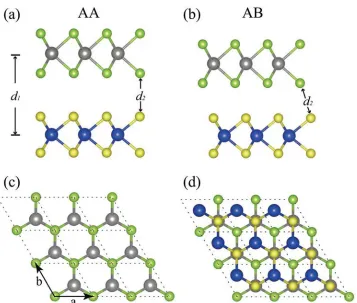
Fig. 1 Atomic structure of AA stacking and AB stacking hetero-bilayer MX2 in a 3 x 3 x 1 supercell from a side view (upper panel) and top view (lower
panel), respectively. Large and small spheres represent the M and X atoms, respectively. Color coding is used to distinguish the different atomic species.
d1 and d2 are the interlayer distance (M1–M2) and the bond length of X1–X2, respectively.
have been studied widely.51 For 2H-phase MX2 crystals, the M
atoms and X atoms are located in different layers, which can be
described by the point group D3h. While for the 3R-phase unit
cell shown as Fig. 1(b and d), one M atom is eclipsed by the X atoms above and the other one is located in the hexagonal center, leading to the AB Bernal stacking. In fact, the electronic
structure of the MX2 heterostructure is sensitive to the stacking
modes, due to the different interlayer interactions. AA and AB
which provides a simple universal form for the relationship
between binding energy and atomic separation.55,56 The
optimized interlayer distance is predicted from a series of
unrelaxed models with different values of d1 (from 5 to 8 Å).
We then calculate the surface adhesion energy Wad for all
30 types of 2D vdW MX2 heterostructure under investigation
here (e.g. MoS2/WSe2 hetero-bilayer),
EMoS þ EWSe - EMoS =WSe
stacking structures possess the weakest and strongest interlayer
electronic coupling, respectively.52 For simplicity, we only consider
Wad ¼ 2 2 2 ; (2)
A
these two stacking modes. However, some interesting properties, where A is the interface area and EMoS , EWSe and EMoS /WSe are
2 2 2 2
e.g. the relatively constant change in both electronic and mechan- ical couplings at twist angles between 01 (AA stacking) and 601 (AB
stacking) found in twisted MoS2 bilayers53 and so on, may not be
captured by these two modes and are beyond the scope of our work. One stacking type can be geometrically transformed to the other by horizontal sliding or by rotation around the vertical
axis. For MX2 heterostructures with two different constituent
monolayer MX2 crystals, both AA and AB stacking crystals
possess a lower symmetry of C3v point group, with the symme-
try operations of C3 and vertical mirror reflection s 54 rather
than the mirror reflection operation sh in the horizontal plane.
To determine the energetically stable structure before geo- metry optimization, an interlayer-distance optimization algorithm
is implemented to reach an optimized d1 (defined in Fig. 1(a))
using the universal binding energy relation (UBER) method,
the total energies of the monolayer MoS2 and WSe2 and the
MoS2/Wse2 heterostructure, respectively. The optimal interlayer
distances d1 can be obtained by maximizing the value of Wad.
Then, further structure optimizations are implemented without any external constraints. Furthermore, the formation energies
E (E = EAB - EA - EB) are listed in Table S2 (ESI†). The negative
values for the formation energies also confirm the stability of
our structures and, for most MX2 heterostructures, AA stacking
is more energetically favorable.
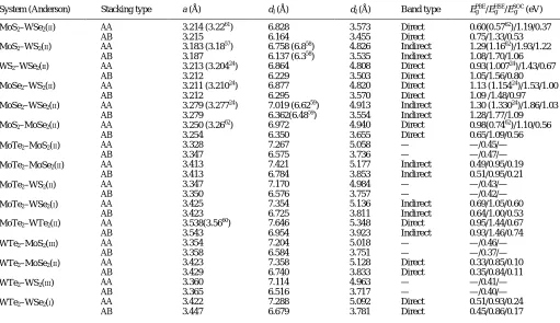
The calculated lattice constants a and interlayer distances d
for the above-mentioned 30 types of 2D MX2 heterostructure are
summarized in Table 1 and are in good agreement with
previous theoretical and experimental results.57–60 As shown
in Table 1, the optimized interlayer distances of AA stacking structures are larger than those of the corresponding AB
Table 1 Hetero-bilayer system and band alignment type, optimized lattice constant a (Å), interlayer distance d1 (Å), the atomic distance d2 (Å) between
the adjacent anion in different layers and the band gap of MX2 heterostructures (PBE/HSE/SOC). Other theoretical data are also listed in parentheses for
comparison
g g g
stacking structures. This is due to the fact that, in AB struc- tures, the X atoms are not aligned along the vertical axis and a shorter interlayer distance leads to a smaller total energy. Furthermore, the change of stacking type of the heterostruc- tures will affect the interlayer interactions of M or X atoms.
3.2 Electronic band structure of hetero-bilayer MX2
Previous studies have revealed that monolayer MX2 possesses a
direct band gap and both the CBM and VBM are located at the K
point in the first Brillouin zone.17,34,63,64 Owing to the lack of
inversion symmetry and the strong spin–orbit coupling (SOC), the valence bands possess a significant spin–orbit splitting at
the K valleys.65 The band alignment for MX2 shows the follow-
ing trends (see Fig. 2(b)): (1) for common-X systems, the band
gaps of MoX2 are larger than that of WX2, and the CBM and
VBM of WX2 are higher than those of MoX2; (2) for common-M
systems, an increase in the atomic number of X results in a shallower anion p orbital and thus a shift of the VBM to higher
Fig. 2 (a) Various possible band-edge lineups in semiconductors A and B. (b) Band alignment for monolayer MX2. The vacuum level is taken
as 0 reference.
.
System (Anderson) Stacking type a (Å) d1 (Å) d2 (Å) Band type EPBE/EHSE/ESOC (eV)
MoS2–WSe2(II) AA 3.214 (3.2261) 6.828 3.573 Direct 0.60(0.5762)/1.19/0.37
AB 3.215 6.164 3.455 Direct 0.75/1.33/0.53
MoS2–WS2(II) AA 3.183 (3.1857) 6.758 (6.858) 4.826 Indirect 1.29(1.1662)/1.93/1.22
AB 3.187 6.137 (6.358) 3.535 Indirect 1.08/1.70/1.06
WS2–WSe2(II) AA 3.213 (3.20424) 6.864 4.808 Direct 0.93(1.00724)/1.43/0.67
AB 3.212 6.229 3.503 Direct 1.05/1.56/0.80
MoSe2–WS2(II) AA 3.211 (3.21024) 6.877 4.820 Direct 1.13 (1.15424)/1.53/1.00
AB 3.212 6.295 3.570 Direct 1.09 /1.48/0.97
MoSe2–WSe2(II) AA 3.279 (3.27724) 7.019 (6.6259) 4.913 Indirect 1.30 (1.33024)/1.86/1.03
AB 3.279 6.362(6.4859) 3.554 Indirect 1.28/1.77/1.09
MoS2–MoSe2(II) AA 3.250 (3.2662) 6.972 4.940 Direct 0.98(0.7462)/1.10/0.56
AB 3.254 6.350 3.655 Direct 0.65/1.09/0.56
MoTe2–MoS2(II) AA 3.328 7.267 5.058 — —/0.45/—
AB 3.347 6.575 3.736 — —/0.47/—
MoTe2–MoSe2(II) AA 3.413 7.421 5.177 Indirect 0.49/0.95/0.19
AB 3.413 6.784 3.853 Indirect 0.51/0.95/0.21
MoTe2–WS2(II) AA 3.347 7.170 4.984 — —/0.43/—
AB 3.350 6.576 3.757 — —/0.42/—
MoTe2–WSe2(I) AA 3.425 7.354 5.136 Indirect 0.69/1.05/0.60
AB 3.423 6.725 3.811 Indirect 0.64/1.00/0.53
MoTe2–WTe2(II) AA 3.538(3.5660) 7.646 5.348 Direct 0.95/1.44/0.67
AB 3.543 6.954 3.923 Indirect 0.93/1.46/0.74
WTe2–MoS2(III) AA 3.354 7.204 5.018 — —/0.46/—
AB 3.358 6.584 3.751 — —/0.37/—
WTe2–MoSe2(II) AA 3.423 7.358 5.128 Direct 0.33/0.85/0.10
AB 3.429 6.740 3.833 Direct 0.35/0.84/0.11
WTe2–WS2(III) AA 3.360 7.114 4.963 — —/0.41/—
AB 3.365 6.516 3.717 — —/0.40/—
WTe2–WSe2(I) AA 3.422 7.288 5.092 Direct 0.51/0.93/0.24
[image:6.596.58.540.517.686.2]energy levels, finally leading to decreased band gaps.66 To understand these two trends in band alignment, the atomic orbital composition of the states should be taken into
consideration. Taking MoS2 as an example, the CBM of MoS2 is
mainly composed of the dz2 orbital of Mo and the px and py
orbitals of S, whereas the VBM mostly consists of the dx2–y2 and
dxy orbitals of Mo.
For the hetero-bilayer MX2 crystals constructed from two
MX2 monolayers, the formation of their band structures can be
understood by the so-called Anderson’s rule, which provides a scheme for the construction of energy band diagrams for
heterostructures consisting of two semiconductor materials.67
According to Anderson’s rule, the vacuum energy levels of the two constituent semiconductors on either side of the
heterostructure should be aligned at the same energy,68 and
[image:7.596.67.519.199.659.2]there are three types of possible band-edge lineups: straddling, staggered and broken gap, as shown in Fig. 2(a). For type I heterostructures, the CBM and VBM mainly consist of the orbitals of semiconductor B, which possesses a smaller band gap compared to semiconductor A. Thus, the band type of the heterostructure is consistent with the smaller-gap material. For type II heterostructures, the VBM and CBM around the Fermi
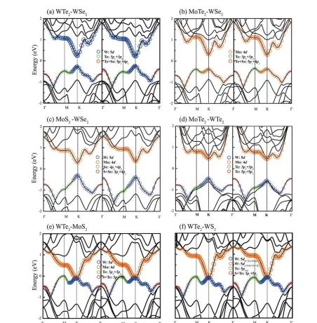
Fig. 3 Band structures of the AA and AB stacking vdW MX2 heterostructures and atomic orbital weights in the energy bands. The blue and orange circles
represent d orbitals of the cations. The green and red circles represent px + py and pz orbitals of the anions, respectively. The size of each
circle is proportional to the weight of the atomic orbital. (a and b) Type I band alignment system: WTe2–WSe2 and MoTe2–WSe2 hetero-bilayer.
(c and d) Type II band alignment system: MoS2–WSe2 and MoSe2–WSe2 hetero-bilayer. (e and f) Type III band alignment system: WTe2–MoS2 and WTe2–
level reside in two separate semiconductors, and the formed heterostructure still possesses a small direct or indirect band gap. As for type III heterostructures, the locations of the CBM and VBM are similar to those of type II heterostructures, but band gap does not exist, and the formed heterostructure is a semi-metal. It should be noted that, for type II and type III
heterostructures, since the CBM and VBM may locate in differ-
ent semiconductors, the photon-generated excitons are thus spatially separated, which will suppress the recombination of electron–hole pairs and extend the exciton lifetime compared
with the corresponding individual semiconductors.26,27,34,69–71
The band structures for the vdW MX2 heterostructures are
calculated using the PBE and HSE06 method and the results,
i.e., band types and band gaps, are shown in Table 1. The direct
band gap at the K point for monolayer MX2 is transformed into
three types of band gap when a hetero-bilayer MX2 crystal is
formed, i.e., direct, indirect (M–K, G–K, K–Q) and zero band
gap or overlapping bands, according to the calculated results shown in Table 1 and the above-mentioned analyses based on Anderson’s rule. The formation types of band gap for the
vdW MX2 heterostructures categorized according to Anderson’s
rule are also shown in Table 1. The classification of the band types according to Anderson’s rule is called as Anderson band type hereafter. It is shown in Table 1 that the Anderson
band types for the vdW MX2 are determined by the constituent
monolayer MX2 irrespective of the stacking manner. This is
probably due to the fact that the VBM/CBM of the hetero-bilayer structure is attributed to the d/p-orbitals of M/X atoms, and the weak vdW interactions will not change the charge distribution of the constituent monolayers significantly, thus the relative CBM/VBM energies of the constituent monolayers will not change.
For simplicity, we first consider the Anderson band type I
heterostructure, e.g. band structures for WTe2–WSe2 and MoTe2–
WSe2 hetero-bilayers, shown in Fig. 3(a and b). Generally, as we
mentioned above, two monolayer MX2 crystals with identical M
atoms but different X atoms possess different CBM/VBM energy levels, and the crystal with the X atoms with the larger atomic number has a higher energy level CBM or VBM. However, as
shown in Fig. 2(b), the CBM energy level of WTe2 is lower than
that of WSe2, although the atomic number of Te is larger than
Se. Such a deviation can be understood by the fact that the bond
length dW–Te of WTe2 is the largest one among those of the
monolayer MX2 crystals, which leads to a small overlap integral V
between the d orbitals of the M atoms and the p orbitals of the
X atoms for the formation of the CBM due to V p 1/dW–Te2,72,73
and thus counteracts the increase of the CBM energy level from
Se with smaller p orbitals compared to Te.34 The smaller CBM
energy level of WTe2 ultimately results in the Anderson band
type-I alignment of band edges in the WTe2–WSe2 hetero-bilayer,
leading to a direct band gap at the K point for both AA and AB
stacking manners, as shown in Fig. 3(a).
According to Table 1, most of the hetero-bilayer MX2 crystals
are Anderson band type II heterostructures, e.g., hetero-bilayer
MoS2–WSe2 and MoTe2–WTe2. Fig. 3(c) shows the energy band
structures of the AA and AB stacking MoS2–WSe2 hetero-
bilayers, exhibiting direct band gaps of 0.60 eV and 0.75 eV for the AA and AB stacking types, respectively, which are
consistent with the previous results.33 The CBM locates in the
MoS2 layer and the VBM locates in the WSe2 layer, resulting
in the formation of spatially separated electron–hole pairs.
Experiments on hetero-bilayer MoS2–WSe2 revealed the dramatic
quenching of the photoluminescence (PL) intensities28 and the
[image:8.596.72.539.442.685.2]extended exciton lifetime.27
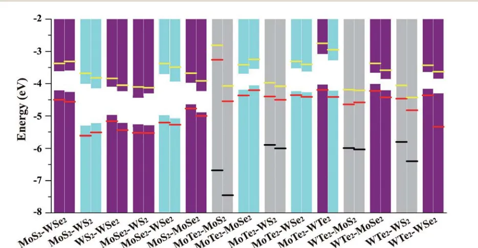
Fig. 4 Calculated band alignment for the vdW MX2 heterostructures. The histogram is obtained by PBE, with the purple, blue and grey representing the
2D ¼ 78
2 As for the formation of indirect band gaps for type-II
heterostructures, there are three types of such indirect band
gap, i.e. M–K, G–K and K–Q, resulting from the relatively higher
energy level of the Te-5p orbital, the relatively stronger pz–pz
bonds of X atoms in different monolayers and the hybridization of M-d and X-p orbitals, respectively.
As shown in Fig. 3, the valence band at the M point is
attributed to the px and py orbitals of X atoms, and the
corresponding energy level for hetero-bilayer MX2 crystals
containing Te atoms is larger than those only containing Se or S atoms, since the atomic number of Te is the largest one.
Therefore, for hetero-bilayer MTe2–MX2, the valence band
energies at the M point significantly increase compared with
the hetero-bilayer MSe2–MX2 (X a Te) or MS2–MX2 (X a Te),
which subsequently leads to the formation of the M–K indirect
band gap, e.g. hetero-bilayer MoTe2–WSe2, as shown in Fig. 3(b).
The valence band at the G point can be attributed to the
inter-layer overlap integral of pz orbitals of X atoms belonging to
different monolayers at the G point, as shown in Fig. 3. For
hetero-bilayer MX2 considered here, the distance between X
atoms in different monolayers for the AB stacking hetero-
bilayer, i.e. d2 shown in Fig. 1(a and b), is smaller than the
corresponding AA stacking hetero-bilayer, as shown in Table 1,
thus the energy level of the valence band at the G point for the
former is the higher one, due to Vp –p p 1/d22. The increase of
WTe2–MoS2 and WTe2–WS2 crystals as shown in Fig. 3(e and f),
are replaced by direct band gaps based on HSE calculations,
which means that the hetero-bilayer MX2 crystals considered here
do not possess Anderson band type III alignment.
In summary, the CBM state at the K point is weakly localized
and not usually affected by the stacking types. The VBM may
shift from the K to G point in regard to different stacking types
due to the interlayer electronic coupling. Kang et al. have stated
that the interlayer coupling strength of the AB configuration at
the G point is the strongest among the heterostructures with
arbitrary in-plane angular rotations to push the band energy at
the G point up to a highest level.75 In contrast, the interlayer
coupling strength of AA configuration (0 degree) is the weakest.
This argument can be proved by the Moir´e pattern of these
heterostructures to demonstrate that the pattern becomes
smaller and more complex with the rotation angle y increasing.
Moreover, this Moir´e pattern-induced wave function localiza-
tion of the VBM will significantly affect the carrier mobilities of
MX2 heterostructures and will be discussed in the next section.
3.3 Mechanical properties and transport properties of hetero- bilayer MX2
Since the MX2 heterostructures under consideration here pos-
sess C3v symmetry, the number of independent second-order
elastic coefficients cij is five and c11 = c22.76 The calculated
z z
the energy level of the valence band at G points sometimes
leads to the formation of G–K indirect band gaps with AB
stacking, e.g. AB-stacking MoTe2–WTe2 as shown in Fig. 3(d).
elastic coefficients of all MX2 heterostructures are shown in
Table S2 (ESI†) and all the vdW MX2 heterostructures are
mechanically stable, according to the Born criteria:77
Another indirect band gap (K–Q), e.g. MoSe2–WSe2 shown in
Fig. S2 (ESI†), is formed by the VBM located at the K point and C11 - C12 4 0, C11 + 2C12 4 0, C44 4 0 (3)
the CBM located at the Q point between G and K. According to
the analysis on the atomic orbitals, the energy level of the 2D The 2D Young’s moduli of all MXc11c22 - c 78 2 heterostructures, given by
valence band at the Q point is formed by the strong hybridiza- Y ¼ c
11 12 , are listed in Table 2. The 2D Young’s
tion between the Mo-d orbitals and W-d orbitals, which lowers
the energy level at the Q point and ultimately leads to the shift
modulus for monolayer MX2 crystals decreases from MS2 to
MSe2 to MTe2,79 which is due to the fact that the strength of
of the CBM from the K to Q point.74 However, the CBM and d –p orbital coupling, which forms M–X bonding, becomes
VBM at K are insignificantly hybridized, due to the higher
symmetry and a larger bond length dMo–W compared to those
at the Q point,57 thus the VBM is fixed at the K point.
The extreme state of staggering is the formation of broken band gaps, which is also known as the Anderson band type III alignment, as shown in Fig. 2(a). For example, the CBMs
of MoS2 and WS2 are much lower than those of other MX2
monolayers and WTe2 possesses the highest VBM, as shown in
Fig. 2(b). The band alignment in hetero-bilayer WTe2–MoS2
and WTe2–WS2 thus can be approximately considered as the
Anderson band type III alignment, as shown in Fig. 3(e and f).
The band overlaps at the K point, changing the heterostructures
into metallic phase.
The band gaps of the hetero-bilayer MX2 crystals based on
the HSE06 and SOC calculations are also provided in Table 1
and Fig. 4. The negative SOC effects decrease the band gap and
the HSE calculations increase the band gap by 0.4–0.6 eV, compared to the PBE calculations. It should be noted that the
metallic phases of the hetero-bilayer MX2 crystals, i.e. the
Anderson band type III heterostructures, e.g. hetero-bilayer
xy,yz,zx
weaker with an increase of the atomic number of chalcogen.80
The calculated 2D Young’s moduli for monolayer MX2 crystals are
shown in Table S1 (ESI†). The contributions to the mechanical
properties of MX2 heterostructures can be roughly considered
from constituent monolayer MX2 crystals and the weak interlayer
bonding.
The Young’s moduli of the MTe2–MX2 heterostructures
are lower than others due to the weakest Y2D of monolayer
MTe2 among the monolayer MX2 crystals considered here.
Meanwhile, the Young’s moduli of the MX2 heterostructures
are a little lower than the sum of those of the constituent
monolayer MX2 crystals, which means that the contribution
from the interlayer bonding to the total Young’s modulus is
c12
negative. The Poisson’s ratio is given by v , which
c22
describes the lateral deformation when applying uniaxial strains, is calculated and shown in Table 2. Generally materials with a high Poisson’s ratio possess good plasticity. The Poisson’s
ratios for the MX2 heterostructures are numerically close
l
Table 2 Hetero-bilayer system and band alignment type, Young’s modulus Y (GPa), Poisson’s ratio v, electron and hole effective masses along the
armchair direction, deformation potential constants for CBM and VBM, elastic modulus and electron and hole mobilities along armchair direction. System
l l
AB 197.77 0.22 0.30 0.45 2.79 3.08 115.65 875.3 918.66
of 0.20 of monolayer WTe2 crystal among the monolayer MX2
crystals (see Table S1, ESI†).
The effective masses for electrons me* and holes mh* of vdW
MX2 heterostructures along armchair and zigzag directions are
calculated, and the results along the armchair direction are
shown in Table 2. The values of me* for AA-stacking MX2
heterostructures are close to those of the corresponding AB-
stacking ones, however, the values of mh* for AA-stacking
heterostructures are obviously deviated from those of AB-
stacking ones, e.g. MoS2–WS2 and MoTe2–WTe2 heterostruc-
tures, especially when the band types for AA and AB stackings
are different (direct vs. indirect), as shown in Tables 1 and 2.
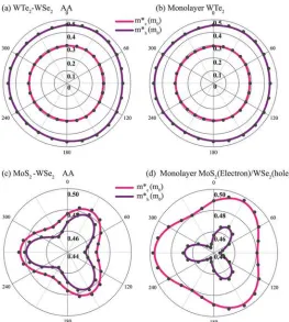
monolayer WTe2 crystal. It is shown in Fig. 5(a and b) that the
effective masses of electrons and holes for the WTe2–WSe2
hetero-bilayer are close to those of monolayer WTe2 crystals.
However, for MoS2–WSe2 hetero-bilayers (Anderson band type II),
since the CBM is attributed to that of monolayer MoS2 crystals
and the VBM is attributed to that of monolayer WSe2 crystals, the
me* value for the MoS2–WSe2 hetero-bilayer is similar to that of
monolayer MoS2 and the mh* value is similar to that of monolayer
WSe2, as shown in Fig. 5(c and d).
According to eqn (1), the third factor determining carrier
mobilities m is the deformation potential constant, De,h, which
describes the scatterings of electrons/holes by longitudinal acoustic
Such phenomena can be understood by the fixed CBM (elec- phonons. The calculated De,h values for MX heterostructures and
l 2
trons) at the K or Q point for all the MX2 heterostructures, and
the transition of the VBM (holes) from the K point to the M or G
point for MX2 heterostructures with an indirect band gap.
As mentioned above, the band structures of MX2 hetero-
structures can be roughly decomposed into those of the con-
stituent monolayer MX2 crystals, according to Anderson’s rule,
which also leads to the formation of the effective masses of
electrons and holes for MX2 heterostructures. Fig. 5 shows the
effective masses of electrons and holes for MX2 heterostruc-
tures and the corresponding constituent monolayer MX2 crys-
tals along all directions, taking WTe2–WSe2 and MoS2–WSe2
hetero-bilayer as examples without loss of generality.
The WTe2–WSe2 hetero-bilayer belongs to Anderson band
type I and the CBM and VBM are attributed to those of the
monolayer MX2 crystals are shown in Table 2 and Table S1 (ESI†),
respectively. By comparison, it is found that the deformation
potential constants of MX2 heterostructures are larger overall than
those of the constituent monolayer MX2, which means that the
formation of the vdW MX2 heterostructures increases the electron–
acoustic phonon coupling, leading to the increase of deformation
potential constant Dl, especially for MoS2–WS2 heterostructures.
Since the CBM and VBM of the MX2 heterostructures can be
attributed to the respective band structures of the constituent
monolayer MX2, according to the Anderson rule, the shift of the
VBM from the K point to the G/M point will result in a dramatic
change of the deformation potential constants and hole effec-
tive masses for MX2 heterostructures with indirect band gaps,
e.g. MoTe2–WTe2. (Anderson)
System (Anderson) Stacking type Y (N m-1) v m
e* (m0) mh* (m0 ) De Dh C (N m
-1) m
e (cm2 (V s) -1) mh (cm2 (V s)-1)
MoS2–WSe2(II) AA 217.58 0.25 0.47 0.47 3.05 3.26 139.55 961.16 875.94
AB 211.03 0.27 0.48 0.46 4.05 2.43 152.92 573.03 1808.89
MoS2–WS2(II) AA 241.46 0.25 0.46 1.70 6.01 5.70 127.81 256.46 18.04
AB 242.03 0.24 0.46 0.92 6.28 5.03 121.19 318.08 76.70
WS2–WSe2(II) AA 229.08 0.26 0.30 0.47 3.44 3.60 149.27 1990.11 770.94
AB 226.75 0.26 0.26 0.45 4.85 2.38 151.14 1345.29 1947.10
MoSe2–WS2(II) AA 261.16 0.31 0.28 0.62 3.26 3.38 152.12 2575.74 511.18
AB 272.66 0.32 0.29 0.58 5.09 1.87 92.47 600.18 1158.73
MoSe2–WSe2(II) AA 218.88 0.27 0.67 0.45 4.29 1.59 130.84 224.10 3752.36
AB 212.42 0.28 0.61 1.12 1.93 2.84 122.16 1239.06 177.56
MoS2–MoSe2(II) AA 232.78 0.26 0.42 0.71 2.87 2.78 125.83 1321.55 454.69
AB 230.26 0.27 0.42 0.71 3.07 4.50 114.86 758.03 359.04
MoTe2–MoS2(II) AA 196.82 0.36
AB 196.87 0.34
MoTe2–MoSe2(II) AA 184.77 0.31 0.46 1.37 4.40 3.74 113.18 532.75 45.79
AB 200.46 0.25 0.46 1.37 4.07 3.75 110.81 532.75 45.79
MoTe2–WS2(II) AA 206.17 0.28
AB 195.86 0.31
MoTe2–WSe2(I) AA 183.70 0.28 0.30 1.33 3.95 3.83 109.1 515.87 52.52
AB 194.71 0.24 0.30 1.25 4.41 4.14 114.79 1191.02 58.76
MoTe2–WTe2(II) AA 136.33 0.39 0.57 0.42 1.61 1.38 101.62 1023.61 55.76
AB 171.83 0.22 0.58 3.46 4.32 3.30 99.43 2315.94 3285.72
WTe2–MoS2(III) AA 169.33 0.20
AB 189.09 0.28
WTe2–MoSe2(II) AA 183.83 0.27 0.45 0.48 2.65 2.85 109.47 382.87 6.58
AB 196.41 0.22 0.45 0.48 2.70 2.85 102.26 912.5 987.31
WTe2–WS2(III) AA 189.00 0.20
AB 233.27 0.29
l
e2ðoÞ ¼ Oe0 k;v;c
[image:11.596.165.428.46.339.2]d Ek - Ek - -ho Ck u · r Ck
Fig. 5 The calculated carrier (hole massh* and electron masse*) for (a) type I band alignment system (WTe2–WSe2 hetero-bilayer), (b) monolayer WTe2,
(c) type II band alignment system (MoS2–WSe2 hetero-bilayer) and (d) monolayer MoS2 (electron) and WSe2 (hole).
In order to figure out the exact contributions from the three
factors, i.e. effective masses me,h*, deformation potential con-
stants De,h and elastic modulus C, to the carrier mobilities m,
compared to the constituent monolayer MX2 crystals, we plot
the values of the three factors for constituent monolayer
crystals and hetero-bilayer structures in Fig. S4 (ESI†). It is
clear that the elastic modulus of hetero-bilayer structures is
nearly twice that of the constituent monolayer MX2 crystals,
while the deformation potential constants of hetero-bilayer structures are larger overall or close to the constituent
monolayer MX2 crystals. Moreover, the effective masses of
hetero-bilayer structures, mostly determined by the constituent monolayer crystals, are close to those of the constituent mono- layer crystals, except some hetero-bilayer structures with VBM
points shifted from K to G/M, e.g. MoTe2–WTe2. Finally, the
carrier mobility of electrons and holes along armchair and
zigzag directions for the MX2 hetero-bilayer can be calculated
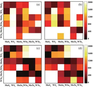
according to eqn (1), as shown in Fig. 6. Fig. 6(a, b) and (c, d) show electron/hole mobilities along armchair and zigzag direc-
tions, respectively. The mobilities for monolayer MX2 as a
overall than those of constituent monolayer MX2 crystals, and
the same situation takes place for the hole mobilities of hetero-
bilayer structures with the VBM located at the K point. However,
the hole mobilities of hetero-bilayer structures with the VBM
located at the G/M point are smaller than those of constituent
monolayer MX2 crystals.
The AA stacked MoTe2–MoSe2 heterostructure possesses
the highest electron mobility along the zigzag direction,
i.e. 3658 cm2 (V s)-1, and the AA stacked MoSe2–WSe2 hetero- structure possesses the highest hole mobility along the
armchair direction, i.e. 3752 cm2 (V s)-1.
3.4 Optical properties of hetero-bilayer MX2
The optical properties of the vdW MX2 heterostructures
are described by the complex dielectric function, i.e. e(o) =
e1(o) + ie2(o). The imaginary part of the dielectric tensor e2(o)
is determined by a summation over empty band states as
follows:81,82
2pe2 X c v c vo 2
spond to the cases of AA/AB-stacking types. For example, the red block of the 1st row and 4th column in Fig. 6(a) corresponds to the electron mobilities along the armchair direction of the
AB-stacking MoS2–WSe2 heterostructure, i.e. m = 573 cm2 (V s)-1.
The electron mobilities of hetero-bilayer structures are larger
where O is the crystal volume, e0 is the vacuum dielectric
constant, -ho represents the photon energy, v and c mean the
valence and conduction bands respectively, u is the polariza-
tion vector in the incident electric field, u·r is the momentum
operator and Ck is the wave function at the k point. The real
contrast are shown as color blocks in the diagonal direction and the color blocks in the lower/upper triangular part corre-
aðoÞ ¼ e 1 2ðoÞ þ e 2 2ðoÞ -e 1 ðoÞ 2; (6)
[image:12.596.141.457.46.342.2]1
Fig. 6 The calculated carrier mobilities for the vdW MX2 heterostructures, with the AA stackings in the lower left corner and AB stackings in the upper right
corner. The values along the diagonal are the mobilities for monolayer MX2.(a and b) The electron mobilities of the vdW MX2 heterostructures along armchair
and zigzag directions, respectively; (c and d) The hole mobilities of the vdW MX2 heterostructures along armchair and zigzag directions, respectively.
part of the dielectric tensor e1(o) is obtained by the well-known pffi
2ffion 1=2 o1
e ðoÞ ¼ 1 þ P
ð1 e2ðo0Þo0 do0; (5) In 2D semiconductor materials, the band gap obtained by
p 0 o02 - o2 þ iZ
where P denotes the principle value. Based on the complex
dielectric function, the absorption coefficient a(o) is given by:84,85
HSE06 is usually close to the real optical band gap due to the underestimation of the band gap by neglecting excitonic
effects.86
[image:12.596.65.535.507.707.2]Thus, we only performed HSE06 calculations to obtain
Fig. 7 HSE06 calculations of (a) the real part of the dielectric function, (b) the imaginary part of the dielectric function and (c) refractive and (d) optical
c c
83 Kramers–Kronig relation:
2
optical properties for the hetero-bilayer MX2 under consideration here, which show that all of them are semiconductors with a finite band gap, as shown in Table 1. All the optical constants are
calculated for incident radiations with the electric field vector E
polarized along the a and b directions,87 as shown in Fig. 1(c).
Due to the C3 symmetry of the hexagonal structure of the
hetero-bilayer MX2, the dielectric function e(o) possesses the
same results along the a and b directions. The e(o) results
for AA and AB stacking types are also close to each other, as
shown in Fig. 7(a and b) and Fig. S4 (ESI†), irrespective of the
corresponding Anderson band type. The similarity in e(o)
results between AA and AB stacking hetero-bilayer MX2 can
be understood by the fact that the band structure of the hetero-
bilayer MX2 can be roughly decomposed into the respective
band structures of the constituent monolayer MX2 according to
Anderson’s rule. Thus, the contribution to the total optical
response, i.e. e2(o), from absorption of an incident photon -ho
and then transition from Cc to Cv, can be traced back to the
Conflicts of interest
There are no conflicts to declare.
Acknowledgements
This work is supported by the National Natural Science Foun- dation of China under grant nos. 11374063 and 11404348, the National Basic Research Program of China (973 Program) under grant no. 2013CBA01505 and FDUROP (Fudan’s Undergraduate Research Opportunities Program) under no. 16066. Work at Ames Laboratory is partially supported by the US Department of
Energy, Office of Basic Energy Science, Division of Materials Science and Engineering (Ames Laboratory is operated for the US Department of Energy by Iowa State University under contract no. DE-AC02-07CH11358). The European Research Council under ERC Advanced grant no. 320081 (PHOTOMETA) supports work at FORTH.
k k
behaviors of electrons located within the constituent mono-
layer MX2. Therefore, the e2(o) results for AA and AB stacking
hetero-bilayer MX2 probably are similar since they contain
identical constituent monolayer MX2, according to eqn (4).
The optical properties of hetero-bilayer MX2, e.g. WTe2–WSe2,
MoS2–WSe2 and WTe2–MoS2, are shown in Fig. 7. The main
absorption peaks of these three hetero-bilayer MX2 locate in the
range of 3.0 to 5.0 eV, i.e. the ultraviolet region, with a refractive
range from 2.80 to 4.27 in this region.
4 Conclusion
In this work, we have investigated the structure and electronic,
mechanical, transport and optical properties of the vdW MX2
heterostructures using first-principles calculations. The AA and
AB stacked hetero-bilayer MX2 exhibit three types of band
alignment according to Anderson’s rule, with a wide band
gap range between 0 and 2 eV. The main differences between
AA and AB stacked hetero-bilayer MX2 lie in the band structure
and mechanical properties due to the interlayer coupling, such
as the indirect G–K band gap. The band structure of MTe2–MX2
will possess a higher valance band at the M point due to the
high band energy of the 5px,y orbitals of Te. The type II band
alignment of the vdW hetero-bilayer MX2 makes interlayer
transitions possible, leading to spatially separated excitons.
The transport properties of the vdW MX2 heterostructures are
consistent with the symmetry of the geometric structures. It should be noted that the carrier mobilities of the hetero-bilayer
MX2 are often higher than those of monolayer MX2, attributed
to the higher elastic modulus for the hetero-bilayer MX2, while
the hetero-bilayer MX2 with an indirect band gap possesses
much lower hole mobilities due to the increased effective masses and deformation potential constants. Furthermore, the calculated optical properties show strong optical absorption
for vdW MX2 heterostructures, enabling novel applications in
optoelectronics from the visible to ultraviolet regions, such as photodetectors, light-emitting diodes and photovoltaics.
References
1 K. S. Novoselov, A. K. Geim, S. V. Morozov, D. Jiang, M. I.
Katsnelson, I. V. Grigorieva, S. V. Dubonos and A. A. Firsov, Two-dimensional gas of massless dirac fermions in graphene,
Nature, 2005, 438, 197–200.
2 H. L. Stormer, Y. Zhang, Y.-W. Tan and P. Kim, Experi-
mental observation of the quantum hall effect and berry’s
phase in graphene, Nature, 2005, 438(7065), 201–204.
3 C. R. Dean, A. F. Young, I. Meric, C. Lee, L. Wang, S. Sorgenfrei,
K.Watanabe, T. Taniguchi, P. Kim, K. L. Shepard and J. Hone,
Boron nitride substrates for high-quality graphene electronics,
Nat. Nanotechnol., 2010, 5(10), 722–726.
4 M. Yankowitz, J. Xue, D. Cormode, J. D. Sanchez-Yamagishi,
K. Watanabe, T. Taniguchi, P. Jarillo-Herrero, P. Jacquod and
B. J. LeRoy, Emergence of superlattice dirac points in graphene
on hexagonal boron nitride, Nat. Phys., 2012, 8(5), 382–386.
5 B. Radisavljevic, A. Radenovic, J. Brivio, V. Giacometti and
A. Kis, Single-layer MoS2 transistors, Nat. Nanotechnol., 2011,
6, 147–150.
6 A. Splendiani, L. Sun, Y. Zhang, T. Li, J. Kim, C.-Y. Chim,
G. Galli and F. Wang, Emerging photoluminescence in
monolayer MoS2, Nano Lett., 2010, 10(4), 1271–1275.
7 D. Xiang, C. Han, J. Wu, S. Zhong, Y. Liu, J. Lin, X.-A. Zhang,
W. P. Hu, B. O¨zyilmaz, A. H. C. Neto, A. T. Shen Wee and
W.Chen, Surface transfer doping induced effective modula-
tion on ambipolar characteristics of few-layer black phos-
phorus, Nat. Commun., 2015, 6, 6485.
8 L. Li, Y. Yu, G. J. Ye, Q. Ge, X. Ou, H. Wu, D. Feng,
X. H. Chen and Y. Zhang, Black phosphorus field-effect
transistors, Nat. Nanotechnol., 2014, 9(5), 372–377.
9 V. Tran, R. Soklaski, Y. Liang and L. Yang, Layer-controlled
band gap and anisotropic excitons in few-layer black phos-
phorus, Phys. Rev. B: Condens. Matter Mater. Phys., 2014,
89(23), 235319.
10 M. Bernardi, M. Palummo and J. C. Grossman, Extra-
photovoltaics using two-dimensional monolayer materials,
Nano Lett., 2013, 13(8), 3664–3670.
11 D. Hennig and C. Mulhern, Collective transport of coupled
particles, Eur. Phys. J. B, 2012, 85(1), 1.
12 W. Zhang, Z. Huang, W. Zhang and Y. Li, Two-dimensional
semiconductors with possible high room temperature
mobility, Nano Res., 2014, 7(12), 1731–1737.
13 T. Cao, G. Wang, W. Han, H. Ye, C. Zhu, J. Shi, Q. Niu,
P. Tan, E. Wang, B. Liu and J. Feng, Valley-selective circular
dichroism of monolayer molybdenum disulphide, Nat.
Commun., 2012, 3(6), 887.
14 H. Zeng, J. Dai, W. Yao, D. Xiao and X. Cui, Valley polarization
in MoS2 monolayers by optical pumping, Nat. Nanotechnol.,
2012, 7(8), 490–493.
15 F. A. Rasmussen and K. S. Thygesen, Computational 2d
materials database: electronic structure of transition-metal
dichalcogenides and oxides, J. Phys. Chem. C, 2015, 119(23),
13169–13183.
16 H. J. Conley, B. Wang, J. I. Ziegler, R. F. Haglund,
S. T. Pantelides and K. I. Bolotin, Bandgap engineering of
strained monolayer and bilayer MoS2, Nano Lett., 2013,
13(8), 3626–3630.
17 K. F. Mak, C. Lee, J. Hone, J. Shan and T. F. Heinz, Atom-
ically thin MoS2: a new direct-gap semiconductor, Phys. Rev.
Lett., 2010, 105, 136805.
18 T. G. Pedersen, C. Flindt, J. Pedersen, N. A. Mortensen, A.-P.
Jauho and K. Pedersen, Graphene antidot lattices: designed
defects and spin qubits, Phys. Rev. Lett., 2008, 100(13), 136804.
19 Q. Liu, L. Li, Y. Li, Z. Gao, Z. Chen and J. Lu, Tuning
electronic structure of bilayer MoS2 by vertical electric field:
a first-principles investigation, J. Phys. Chem. C, 2012,
116(40), 21556–21562.
20 K. S. Novoselov, A. Mishchenko, A. Carvalho and A. H. Castro
Neto, 2d materials and van der Waals heterostructures,
Science, 2016, 353(6298), aac9439.
21 S. J. Haigh, A. Gholinia, R. Jalil, S. Romani, L. Britnell, D. C.
Elias, K. S. Novoselov, L. A. Ponomarenko, A. K. Geim and R. Gorbachev, Cross-sectional imaging of individual layers and buried interfaces of graphene-based heterostructures
and superlattices, Nat. Mater., 2012, 11(9), 764–767.
22 W.-T. Hsu, Z.-A. Zhao, L.-J. Li, C.-H. Chen, M.-H. Chiu, P.-S.
Chang, Y.-C. Chou and W.-H. Chang, Second harmonic generation from artificially stacked transition metal dichal-
cogenide twisted bilayers, ACS Nano, 2014, 8(3), 2951–2958.
23 W. Zhang, Q. Wang, Y. Chen, Z. Wang and A. T. S. Wee, Van
der Waals stacked 2d layered materials for optoelectronics,
2D Mater., 2016, 3(2), 022001.
24 H. Terrones, F. Lo´pez-Ur´ıas and M. Terrones, Novel hetero-
layered materials with tunable direct band gaps by sand-
wiching different metal disulfides and diselenides, Sci. Rep.,
2013, 3(3), 1549.
25 A. Kogar, M. S. Rak, S. Vig, A. A. Husain, F. Flicker, Y. I. Joe,
L. Venema, G. J. MacDougall, T. C. Chiang, E. Fradkin, J. van Wezel and P. Abbamonte, Signatures of exciton condensa-
tion in a transition metal dichalcogenide, Science, 2017,
358(6368), 1314–1317.
26 P. Rivera, J. R. Schaibley, A. M. Jones, J. S. Ross, S. Wu,
G. Aivazian, P. Klement, K. Seyler, G. Clark, N. J. Ghimire, J. Yan, D. G. Mandrus, W. Yao and X. Xu, Observation of
long-lived interlayer excitons in monolayer MoSe2–WSe2
heterostructures, Nat. Commun., 2015, 6, 6242.
27 M.-H. Chiu, C. Zhang, H.-W. Shiu, C.-P. Chuu, C.-H. Chen,
C.-Y. S. Chang, C.-H. Chen, M.-Y. Chou, C.-K. Shih and L.-J. Li,
Determination of band alignment in the single-layer MoS2/
WSe2 heterojunction, Nat. Commun., 2015, 6, 7666.
28 H. Fang, C. Battaglia, C. Carraro, S. Nemsak, B. Ozdol,
J. S. Kang, H. A. Bechtel, S. B. Desai, F. Kronast, A. A. Unal, G. Conti, C. Conlon, G. K. Palsson, M. C. Martin, A. M. Minor, C. S. Fadley, E. Yablonovitch, R. Maboudian and A. Javey, Strong interlayer coupling in van der Waals heterostructures
built from single-layer chalcogenides, Proc. Natl. Acad. Sci.
U. S. A., 2014, 111(17), 6198–6202.
29 X. Hong, J. Kim, S.-F. Shi, Y. Zhang, C. Jin, Y. Sun, S. Tongay,
J. Wu, Y. Zhang and F. Wang, Ultrafast charge transfer in
atomically thin MoS2/WS2 heterostructures, Nat. Nanotechnol.,
2014, 9(9), 682–686.
30 H. Heo, J. H. Sung, S. Cha, B.-G. Jang, J.-Y. Kim, G. Jin, D. Lee,
J.-H. Ahn, M.-J. Lee, J. H. Shim, H. Choi and M.-H. Jo, Interlayer orientation-dependent light absorption and emission in mono-
layer semiconductor stacks, Nat. Commun., 2015, 6(5), 7372.
31 Y. Balaji, Q. Smets, C. J. Lockhart De La Rosa, A. K. Augustin
Lu, D. Chiappe, T. Agarwal, D. H. C. Lin, C. Huyghebaert, I. Radu, D. Mocuta and G. Groeseneken, Tunneling transis-
tors based on MoS2/MoTe2 van der Waals heterostructures,
IEEE J. Electron Devices Soc., 2018, 6, 1048–1055.
32 Y. Chen, X. Wang, G. Wu, Z. Wang, H. Fang, T. Lin, S. Sun,
H. Shen, W. Hu, J. Wang, J. Sun, X. Meng and J. Chu, High-
performance photovoltaic detector based on MoTe2/MoS2
van der Waals heterostructure, Small, 2018, 14(9), 1703293.
33 N. Lu, H. Guo, L. Li, J. Dai, L. Wang, W.-N. Mei, X. Wu and
X. C. Zeng, MoS2/MX2 heterobilayers: bandgap engineering
via tensile strain or external electrical field, Nanoscale, 2014,
6(5), 2879–2886.
34 J. Kang, S. Tongay, J. Zhou, J. Li and J. Wu, Band offsets and
heterostructures of two-dimensional semiconductors, Appl.
Phys. Lett., 2013, 102(1), 012111.
35 G. Kresse and J. Furthmu¨ller, Efficient iterative schemes for
ab initio total-energy calculations using a plane-wave basis set,
Phys. Rev. B: Condens. Matter Mater. Phys., 1996, 54, 11169–11186.
36 J. P. Perdew, K. Burke and M. Ernzerhof, Generalized
gradient approximation made simple, Phys. Rev. Lett.,
1996, 77, 3865–3868.
37 S. Grimme, Semiempirical gga-type density functional con-
structed with a long-range dispersion correction, J. Comput.
Chem., 2006, 27(15), 1787–1799.
38 S. Grimme, J. Antony, S. Ehrlich and H. Krieg, A consistent
and accurate ab initio parametrization of density functional dispersion correction (DFT-d) for the 94 elements h-pu,
J. Chem. Phys., 2010, 132(15), 154104.
39 S. Grimme, S. Ehrlich and L. Goerigk, Effect of the damping
function in dispersion corrected density functional theory,
J. Comput. Chem., 2011, 32(7), 1456–1465.
40 J. Heyd, G. E. Scuseria and M. Ernzerhof, Hybrid functionals
based on a screened coulomb potential, J. Chem. Phys.,
2003, 118(18), 8207–8215.
41 J. Heyd, G. E. Scuseria and M. Ernzerhof, Erratum: Hybrid
functionals based on a screened coulomb potential?, J. Chem.
Phys., 2003, 118, 8207 (J. Chem. Phys., 2006, 124, 219906).
42 L. Tang, M. Q. Long, D. Wang and Z. G. Shuai, The role of
acoustic phonon scattering in charge transport in organic semiconductors: a first-principles deformation-potential
study, Sci. China, Ser. B: Chem., 2009, 52(10), 1646–1652.
43 Y. Cai, G. Zhang and Y. W. Zhang, Polarity-reversed robust
carrier mobility in monolayer MoS2 nanoribbons, J. Am.
Chem. Soc., 2014, 136, 6269–6275.
44 M. Long, L. Tang, D. Wang, Y. Li and Z. Shuai, Electronic struc-
ture and carrier mobility in graphdiyne sheet and nanoribbons:
theoretical predictions, ACS Nano, 2011, 5(4), 2593–2600.
45 J. Chen, J. Xi, D. Wang and Z. Shuai, Carrier mobility in
graphyne should be even larger than that in graphene: a
theoretical prediction, J. Phys. Chem. Lett., 2013, 4, 1443–1448.
46 W. Yanli and Y. Ding, Electronic structure and carrier
mobilities of arsenene and antimonene nanoribbons: a
first-principle study, Nanoscale Res. Lett., 2015, 10, 254.
47 J. Bardeen and W. Shockley, Deformation potentials and
mobilities in non-polar crystals, Phys. Rev., 1950, 80, 72–80.
48 W. Walukiewicz, H. E. Ruda, J. Lagowski and H. C. Gatos,
Electron mobility in modulation-doped heterostructures, Phys.
Rev. B: Condens. Matter Mater. Phys., 1984, 30(8), 4571–4582.
49 S ichi Takagi, J. L. Hoyt, J. J. Welser and J. F. Gibbons,
Comparative study of phonon-limited mobility of two- dimensional electrons in strained and unstrained si metal–
oxide–semiconductor field-effect transistors, J. Appl. Phys.,
1996, 80(3), 1567–1577.
50 J. A. Wilson and A. D. Yoffe, The transition metal dichalco- genides discussion and interpretation of the observed opti-
cal, electrical and structural properties, Adv. Phys., 1969,
18(73), 193–335.
51 G. R. Bhimanapati, Z. Lin, V. Meunier, Y. Jung, J. Cha,
S. Das, D. Xiao, Y. Son, M. S. Strano, V. R. Cooper, L. Liang, S. G. Louie, E. Ringe, W. Zhou, S. S. Kim, R. R. Naik, B. G. Sumpter, H. Terrones, F. Xia, Y. Wang, J. Zhu, D. Akinwande, N. Alem, J. A. Schuller, R. E. Schaak, M. Terrones and J. A. Robinson, Recent Advances in Two-
Dimensional Materials beyond Graphene, ACS Nano, 2015,
9(12), 11509–11539.
52 H. Shu, Y. Li, X. Niu and J. Wang, The stacking dependent
electronic structure and optical properties of bilayer black
phosphorus, Phys. Chem. Chem. Phys., 2016, 18(8), 6085–6091.
53 K. Liu, L. Zhang, T. Cao, C. Jin, D. Qiu, Q. Zhou, A. Zettl,
P. Yang, S. G. Louie and F. Wang, Evolution of interlayer
coupling in twisted molybdenum disulfide bilayers, Nat.
Commun., 2014, 5, 4966.
54 J. L. Birman and G. Burns, Introduction to Group Theory with
Applications, Academic Press, 1977.
55 J. H. Rose, J. Ferrante and J. R. Smith, Universal binding
energy curves for metals and bimetallic interfaces, Phys.
Rev. Lett., 1981, 47(9), 675–678.
56 J. Zhao, Y. Li and J. Ma, Quantum spin hall insulators
in functionalized arsenene (asx, x = f, oh andch3) mono-
layers with pronounced light absorption, Nanoscale, 2016, 8,
9657–9666.
57 S. Gao, L. Yang and C. D. Spataru, Interlayer coupling and
gate-tunable excitons in transition metal dichalcogenide
heterostructures, Nano Lett., 2017, 17(12), 7809–7813.
58 Z. Ji, H. Hong, J. Zhang, Q. Zhang, W. Huang, T. Cao,
R. Qiao, C. Liu, J. Liang, C. Jin, L. Jiao, K. Shi, S. Meng and K. Liu, Robust stacking-independent ultrafast charge
transfer in MoS2/WS2 bilayers, ACS Nano, 2017, 11(12),
12020–12026.
59 B. Amin, N. Singh and U. Schwingenschlæˇzˇsgl, Heterostruc-
tures of transition metal dichalcogenides, Phys. Rev. B:
Condens. Matter Mater. Phys., 2015, 92(7), 075439.
60 Z. Zheng, X. Wang and W. Mi, Strain and electric-field tunable
valley states in 2d van der Waals MoTe2/WTe2 heterostructures,
J. Phys.: Condens. Matter, 2016, 28(50), 505003.
61 B. Amin, T. P. Kaloni, G. Schreckenbach and M. S. Freund,
Materials properties of out-of-plane heterostructures of MoS2–
WSe2 and WS2–MoSe2, Appl. Phys. Lett., 2016, 108(6), 063105.
62 N. Lu, H. Guo, L. Li, J. Dai, L. Wang, W.-N. Mei, X. Wu and
X. C. Zeng, MoS2/MX2 heterobilayers: bandgap engineering
via tensile strain or external electrical field, Nanoscale, 2014,
6(5), 2879–2886.
63 H. Jiang, Electronic band structures of molybdenum and
tungsten dichalcogenides by the GW approach, J. Phys.
Chem. C, 2012, 116(14), 7664–7671.
64 Y. Ding, Y. Wang, J. Ni, L. Shi, S. Shi and W. Tang, First
principles study of structural, vibrational and electronic properties of graphene-like MX2 (m = mo, nb, w, ta; x = s,
se, te) monolayers, Phys. B, 2011, 406(11), 2254–2260.
65 K. Ko´smider and J. Fern´andez-Rossier, Electronic properties
of the MoS2–WS2 heterojunction, Phys. Rev. B: Condens.
Matter Mater. Phys., 2012, 87(7), 216.
66 W. G. Zeier, A. Zevalkink, Z. M. Gibbs, G. Hautier, M. G.
Kanatzidis and G. Jeffrey Snyder, Thinking like a chemist:
intuition in thermoelectric materials, Angew. Chem., Int. Ed.,
2016, 55(24), 6826–6841.
67 R. L. Anderson, Germanium–gallium arsenide heterojunctions
[letter to the editor], IBM J. Res. Dev., 1960, 4(3), 283–287.
68 N. Vol, What is what in the nanoworld: a handbook on
nanoscience and nanotechnology, Materials Today, 2004,
7(12), 49.
69 H. Fang, C. Battaglia, C. Carraro, S. Nemsak, B. Ozdol,
J. S. Kang, H. A. Bechtel, S. B. Desai, F. Kronast, A. A. Unal, G. Conti, C. Conlon, G. K. Palsson, M. C. Martin, A. M. Minor, C. S. Fadley, E. Yablonovitch, R. Maboudian and A. Javey, Strong interlayer coupling in van der Waals heterostructures built from single-layer chal-
cogenides, Proc. Natl. Acad. Sci. U. S. A., 2014, 111(17),
6198–6202.
70 S. Zhang, M. Xie, F. Li, Z. Yan, Y. Li, E. Kan, W. Liu, Z. Chen
and H. Zeng, Semiconducting group 15 monolayers: a broad
range of band gaps and high carrier mobilities, Angew.
Chem., Int. Ed., 2016, 55(5), 1666–1669.
71 M.-H. Chiu, C. Zhang, H.-W. Shiu, C.-P. Chuu, C.-H. Chen, C.-Y. S. Chang, C.-H. Chen, M.-Y. Chou, C.-K. Shih and L.-J. Li, Determination of band alignment in the single-layer
MoS2/WSe2 heterojunction, Nat. Commun., 2015, 6, 7666.
72 B. Peng, H. Zhang, H. Shao, K. Xu, G. Ni, J. Li, H. Zhu and
C. M. Soukoulis, Chemical intuition for high thermoelectric performance in monolayer black phosphorus, alpha-arsenene
and aw-antimonene, J. Mater. Chem. A, 2018, 6(5), 2018–2033.
73 S. Froyen and W. A. Harrison, Elementary prediction of linear
combination of atomic orbitals matrix elements, Phys. Rev. B:
Condens. Matter Mater. Phys., 1979, 20, 2420–2422.
74 A. T. Hanbicki, H.-J. Chuang, M. R. Rosenberger,
C. S. Hellberg, S. V. Sivaram, K. M. McCreary, I. I. Mazin
and B. T. Jonker, Double indirect interlayer exciton in a
MoSe2/WSe2 van der Waals heterostructure, ACS Nano,
2018, 12(5), 4719–4726.
75 J. Kang, J. Li, S.-S. Li, J.-B. Xia and L.-W. Wang, Electronic
structural moir´e pattern effects on MoS2/MoSe2 2d hetero-
structures, Nano Lett., 2013, 13(11), 5485–5490.
76 M. F´elix and F.-X. Coudert, Necessary and sufficient elastic
stability conditions in various crystal systems, Phys. Rev. B:
Condens. Matter Mater. Phys., 2014, 90(22), 224104.
77 B. Peng, H. Zhang, H. Shao, Z. Ning, Y. Xu, G. Ni, H. Lu,
D. W. Zhang and H. Zhu, Stability and strength of atom-
ically thin borophene from first principles calculations,
Mater. Res. Lett., 2017, 5(6), 399–407.
78 R. C. Andrew, R. E. Mapasha, A. M. Ukpong and N. Chetty,
Mechanical properties of graphene and boronitrene, Phys.
Rev. B: Condens. Matter Mater. Phys., 2012, 85(12), 777–782.
79 F. Zeng, W.-B. Zhang and B.-Y. Tang, Electronic structures
and elastic properties of monolayer and bilayer transition
metal dichalcogenides MX2 (m = mo, w; x = o, s, se, te): a
comparative first-principles study, Chin. Phys. B, 2015,
24(9), 097103.
80 L. Yu, Q. Yan and A. Ruzsinszky, Negative poisson’s ratio
in 1t-type crystalline two-dimensional transition metal
dichalcogenides, Nat. Commun., 2017, 8, 15224.
81 M. Gajdoˇs, K. Hummer, G. Kresse, J. Furthmu¨ller and
F. Bechstedt, Linear optical properties in the projector-
augmented wave methodology, Phys. Rev. B: Condens. Matter
Mater. Phys., 2006, 73, 045112.
82 Y. Xu, B. Peng, H. Zhang, H. Shao, R. Zhang and H. Zhu, First-
principle calculations of optical properties of monolayer
arsenene and antimonene allotropes, Ann. Phys., 2017, 1600152.
83 M. S. Dresselhaus. Solid State Physics Part II Optical Proper-
ties of Solids, Citeseer, 1999.
84 S. Saha, T. P. Sinha and A. Mookerjee, Electronic structure,
chemical bonding, and optical properties of paraelectric batio3,
Phys. Rev. B: Condens. Matter Mater. Phys., 2000, 62, 8828–8834.
85 B. Luo, X. Wang, E. Tian, G. Li and L. Li, Electronic
structure, optical and dielectric properties of batio3/catio3/
srtio3 ferroelectric superlattices from first-principles calcu-
lations, J. Mater. Chem. C, 2015, 3, 8625–8633.
86 J.-H. Yang, Y. Zhang, W.-J. Yin, X. G. Gong, B. I. Yakobson
and S.-H. Wei, Two-dimensional sis layers with promising electronic and optoelectronic properties: theoretical predic-
tion, Nano Lett., 2016, 16(2), 1110–1117.
87 Y. Xu, H. Zhang, H. Shao, G. Ni, J. Li, H. Lu, R. Zhang,
B. Peng, Y. Zhu, H. Zhu and C. M. Soukoulis, First- principles study on the electronic, optical, and transport
properties of monolayer alpha- and beta-GeSe, Phys. Rev. B,