MURDOCH RESEARCH REPOSITORY
Feng, C., Liang, J. and Agelidis, V.G. (2007) Modified
phase-shifted PWM control for flying capacitor multilevel converters.
IEEE Transactions on Power Electronics, 22 (1). pp. 178-185.
Copyright © 2006 IEEE
Personal use of this material is permitted. However, permission to reprint/republish
this material for advertising or promotional purposes or for creating new collective
Modified Phase-Shifted PWM Control for
Flying Capacitor Multilevel Converters
Chunmei Feng
, Member, IEEE
, Jun Liang
, Member, IEEE
, and Vassilios G. Agelidis
, Senior Member, IEEE
Abstract—The issue of voltage imbalance remains a challenge for the flying capacitor multilevel converter. The phase-shifted pulsewidth modulation (PS–PWM) method has a certain degree of self-balancing properties. However, the method alone is not sufficient to maintain balanced capacitor voltages in practical applications. The paper proposes a closed-loop modified PS–PWM control method by incorporating a novel balancing algorithm. The algorithm takes advantage of switching redundancies to adjust the switching times of selected switching states and thus maintaining the capacitor voltages balanced without adversely affecting the system’s performance. Key techniques of the proposed control method, including selection of switching states, calculation of adjusting times for the selected states, and determination of new switching instants of the modified PS–PWM are described and analyzed. Simulation and experimental results are presented to confirm the feasibility of the proposed method.
Index Terms—Flying capacitor (FC) converter, modified phase-shifted pulsewidth modulation (PS–PWM), multilevel converter, voltage balancing.
I. INTRODUCTION
M
ULTILEVEL converters synthesize voltage waveformsusing a number of semiconductor devices connected in a special arrangement, which are typically rated at a fraction of the dc bus voltage. The unique structure of these multilevel converters makes them suitable for high voltage and high power applications such as flexible alternating current transmission systems (FACTS), high voltage direct current (HVDC), and large electric adjustable speed motor drive (ASMD). These converters are able to generate output voltage waveforms with lower harmonic distortion, lower electromagnetic interference (EMI) and higher efficiencies when compared with the conven-tional topologies [1]–[3].
There are three types of multilevel converter topologies, namely, the neutral-point-clamped (NPC) converter [4], the flying capacitor (FC) converter [5], and the cascaded con-verter with separate dc voltage sources (also called H-bridge
Manuscript received September 27, 2005; revised March 13, 2006. This work was supported by the UK Engineering and Physical Sciences Research Council (EPSRC). Recommended for publication by Associate Editor A. Von Juanne.
C. Feng is with the Department of Electrical and Electronic Engineering, Im-perial College, London SW7 2AZ, U.K. (e-mail: [email protected]).
J. Liang is with the School of Electronics, University of Glamorgan, Glam-organ CF37 1DL, U.K. (e-mail: [email protected]).
V. G. Agelidis is with the School of Electrical, Energy and Process Engineering, Murdoch University, Murdoch 6150, Australia (e-mail: [email protected]).
Color versions of one or more of the figures in this paper are available online at http://ieeexplore.ieee.org.
Digital Object Identifier 10.1109/TPEL.2006.886600
converter) [6]. The FC converter has attracted a great deal of interest in recent years mainly due to a number of advanta-geous features. For instance, it seems that the extension of the converter to higher than three levels is possibly easier than the NPC alternative in commercial applications [7], [8]. However, a number of drawbacks need to be further addressed. These include large capacitor banks, additional precharging circuitry, and in particular voltage imbalance amongst FCs.
The balancing of FC voltages is quite important and dic-tates both the safe and efficient operation of the converter [9]. If voltage imbalance occurs, the quality of the output voltages will deteriorate and blocking voltages imposed on certain de-vices may increase beyond the rated values. Thus, the safe op-eration of power devices cannot be guaranteed. Therefore, it is necessary to take into account the balance of FC voltages when designing the control schemes for the FC converters.
Different control strategies taking the capacitor voltage bal-ancing into account have been proposed for FC converters op-erating in various applications. A direct staircase angle con-trol was introduced in [10]. It is adapted for those applications where the typical pulsewidth modulation (PWM) control does not exist, such as direct torque control (DTC) and sliding mode control or hysteresis control. A carrier-rotation PWM technique was proposed in [11]. However, the above two control methods only deal with the open-loop control. If the small imbalance situation occurs, a compensation algorithm is also needed. A closed-loop control strategy based on an exact linearization and capacitor voltage estimation has been presented in [12]. It re-mains attractive for dc–dc conversion as it reduces the number of sensors in the converter system. However, its design and imple-mentation becomes complicated and output voltage waveform is affected when applied to dc–ac inverters. The phase-shifted PWM (PS–PWM) method also has a self-balancing property. It has been widely used for the multilevel FC converter since its implementation is straightforward [13]. However, in practical systems, capacitor voltages may diverge from their balanced values due to non-ideal conditions and disturbances, such as un-equal capacitance leakage currents, unun-equal delays in switching, asymmetrical charging/discharging of capacitors and load dis-turbances. Thus, an external control loop, besides the PS–PWM method is needed to balance the voltage of the capacitors. The integration of an external loop with self-balancing properties is an issue that needs to be further investigated [7].
Some technical papers have presented voltage balancing strategies for FCs based on the PS–PWM method. Specifically, an extra “balance booster” was proposed in [14], which is an filter with a natural frequency equal to the switching frequency to improve the dynamics of rebalancing. It has the advantage of being reliable but the extra filter increases the cost of the overall system and its power losses especially in
Fig. 1. Phase-leg of a five-level FC multilevel converter.
high-voltage applications.Reference [15] proposed a method to either charge or discharge the FCs by switching on switch pairs of positive and negative legs of the multilevel bridge simultaneously for a very short period to maintain capacitor voltages. This method could lead to extremely high short-cir-cuit currents. In [16], a control strategy for five-level multilevel FC converters based on the idea of introducing corrected modulation waveform by adding square-wave type signals was proposed. This control approach can be easily incorporated into the phase-shifted PWM method, but with negative effect on the output waveform. A feedback control scheme was proposed for the voltage stabilization by adding or subtracting duty cycles in proportion to the unbalanced portion [17]. However, it is only suitable for three-level converters with only one FC. For higher-level converters, it is hard to describe the nonlinear rela-tionship between the output current and the capacitor voltages. In addition, there exists interaction among multicapacitors which makes it impossible to control the output current and the capacitor voltages simultaneously by just simply adjusting the respective duty cycles.
The objective of this paper is to present a closed-loop control strategy which consists of the conventional PS–PWM method and a novel voltage balancing control algorithm. The proposed approach is quite different from the above mentioned methods. Specifically, the algorithm utilizes the redundancy of FC con-verter switching states to change the charge/discharge times of capacitors. In addition, by properly selecting the combinations of the switching states, the method decouples the control of multiple capacitors. Thus, it can control capacitor voltages in-dependently. Moreover, this approach does not introduce any
TABLE I
FIVE-LEVELFC CONVERTERVOLTAGELEVELS ANDTHEIRSWITCHINGSTATES
1: switch on; 0: switch off;
+: charging mode;0: discharging mode;N: no change. Charging/discharging modes of FCs in this table are obtained assumingi >0. These modes are interchanged fori <0.
extra harmonic distortion in the output voltage waveform. Even though the proposed control scheme is applied to a five-level FC converter in this paper, it can be extended to higher-level FC converters.
The paper is organized in the following way. Section II de-scribes the basic structure of the five-level FC converter and its operating principle. The conventional PS–PWM method is briefly introduced in Section III. Section IV addresses the pro-posed voltage balancing control algorithm. Simulation and ex-perimental results with and without the proposed closed-loop control strategy are given in Sections V and VI, respectively, in order to illustrate the validity of the method. Finally, conclu-sions are summarized in Section VII.
II. FC MULTILEVELCONVERTER
A phase leg of a five-level FC multilevel converter is shown in Fig. 1. It is vital for the proper functioning of this converter
that all FCs, namely, , , and to be charged to 4,
2, and 3 4, respectively. Consequently, the voltage
stress across any switch in this circuit equals 4. The most
attractive feature of the FC converter is that the voltage synthesis in an FC converter has more flexibility than that of the NPC topology. For a given voltage level, there are several switching
states that give the same output voltage , but result in different
charging or discharging modes for the FCs. This is also known as switching redundancy. Table I lists five-level FC converter’s voltage levels and all the charging/discharging modes of each
FC for 0. It should be noted that charging/discharging
modes of capacitors are interchanged for 0. For the analysis
in this paper, the instantaneous load current is assumed to be
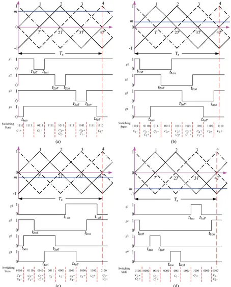
Fig. 2. Control signals for different modulating reference values. (a) 0.5 pu.< m 1.0 pu.; (b) 0 pu.< m 0.5 pu.; (c) 00.5 pu.< m 0 pu.; (d) 01 pu.< m 00.5 pu.
switch pairs in each phase leg , ,
and , respectively, but only the upper four switches
are given in Table I.
III. PHASE-SHIFTEDPWM METHOD
This concept was first proposed in [18]. For a five-level FC converter, a reference modulation signal is compared with four
triangular carrier signals that are phase shifted by 90 . The re-sulting PWM signals control the corresponding switches.
Fig. 2 illustrates the conventional PS–PWM method applied to a five-level FC converter. It is assumed that the frequency
modulation ratio is sufficiently large so that the modulating
reference value can be regarded as a constant in a switching
Fig. 3. Building block of the voltage balancing controller.
shown in Fig. 2(a)–(d), respectively. The control switching
sig-nals , , , and for the main switches of to as
well as switching states and associated capacitor charging and discharging modes are also shown in Fig. 2.
PS–PWM can maintain the capacitor voltage to a certain de-gree by applying equal time duration of the charging and the discharging switching states for each capacitor. Thus, PS–PWM has a self-balancing property. However, voltage imbalance of FCs in practical implementations may still occur due to unequal parameters of the converter caused by different IGBT
toler-ances, different and different value of the FCs, etc.
There-fore, a feedback loop is required to eliminate the accumulative error and make the capacitor voltages stabilize at the desired ref-erence values.
IV. PROPOSEDCONTROLALGORITHM FOR FLYING
CAPACITORVOLTAGEBALANCING
A. Building Block of the Voltage Balancing Controller
The voltage balancing controller is shown in Fig. 3. It consists of proportional integral (PI) controllers and a balancing control algorithm. This novel algorithm is introduced in this section.
Here, the reference voltages , , and for the three
FCs in the five-level FC converter are 4, 2, and 3 4,
respectively. The actual average values of , , and
measured by sensors are compared with their reference values and then the errors are fed into the PI controllers. The outputs of the PI controllers are multiplied with the sign of the output
current and finally generate the adjusting time , ,
and for the FCs , , and , respectively. The load
current direction must be considered since it determines the capacitor charging or discharging mode for the same switching state.
The implementation procedure of the balancing control algo-rithm can be summarized as follows.
Step 1: Selecting the related switching states to be adjusted for compensating the voltage variation for every FC in terms of different regions.
Step 2: Calculating the adjusting time for every selected
switching state taking , , and into
ac-count.
Step 3: Adjusting the time duration of every selected switching state and determining switching instants.
B. Implementation of the Novel Voltage Balancing Control Algorithm
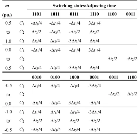
Step 1: As illustrated in Fig. 2, there are four regions in terms
of . For every region, different switching states are selected to
compensate the capacitor voltage variations. Taking the region
0.5 pu. 1.0 pu. as an example, five switching states
are available according to PS–PWM, namely 1110, 1111, 0111,
1011, and 1101, as shown in Fig. 2(a). Assuming is lower
than its reference value, it is required to increase while not
affecting and . One possible way is just to increase the
time duration of 1110 so as to increase the charging time of
and thus to increase . However, increasing the 1110
dura-tion decreases the 1111 duradura-tion, and the duty cycle is changed, thus the output voltage is affected through this simple adjust-ment. To ensure the output voltage is not affected, all of the switching instants in a switching cycle need to be considered to
force to return back to its reference value without affecting
, and the output voltage as well. It can be seen from the
Table I that the switching state 1101 discharges and charges
in this region. We can reduce the time duration of this state
by 4 so that the discharge time is reduced by 4
which increases . However, such an adjustment affects
since it shortens the charging time of . To compensate that,
the 1011 switching state can be shortened by 4. The
adjust-ment of the state 1011 in turn decreases . Then, we can
com-pensate the variation of by shortening the 0111 switching
state by 4. Therefore, by shortening the switching states
1101, 1011, and 0111 by 4, respectively, is increased
without affecting and values. Finally, in order to keep
the duty cycle in a switching period unchanged, the duration of
the switching state 1110 must be increased by 3 4, which
further increases the charging time of and . The adjusted
waveforms are shown in Fig. 4.
Similarly, and can be adjusted through selecting the
appropriate switching states. When the modulating reference value is between 0.5 and 1.0 pu., their adjustment procedure can be explained as follows.
If is lower than its reference value, then:
• reduce the time duration of the state 1101 by (i.e.,
discharging time decreases, charging time also
de-creases);
• reduce the time duration of the state 1011 by 4 (i.e.,
discharging time decreases, charging time also
de-creases);
• reduce the time duration of the state 0111 by 4 (i.e.,
discharging time decreases);
• increase the time duration of the state 1110 by 3 4 (i.e.,
charging time increases).
If is lower than its reference value, then:
• increase the time duration of the state 1101 by 2 (i.e.,
charging time increases, discharging time also
in-creases);
• increase the time duration of the state 1110 by 2 (i.e.,
charging time increases);
• reduce the time duration of the state 1011 by 2 (i.e.,
discharging time decreases, charging time also
de-creases);
• reduce the time duration of the state 0111 by 2 (i.e.,
Fig. 4. Expanded view of selected switching waveforms after adjustment.
If is lower than its reference value, then:
• increase the time duration of the state 1011 by 4 (i.e.,
charging time increases, discharging time also
in-creases);
• increase the time duration of the state 1101 by 4 (i.e.,
charging time increases, discharging time also
in-creases);
• increase state 1110 length by 4 (i.e., charging time
increases);
• reduce state 0111 length by 3 4 (i.e., discharging
time decreases).
The adjusting times of selected switching states for all four regions are summarized in Table II. The overall adjusting times during a switching period for any region is zero in order to avoid changing the output voltage and affecting the overall system characteristics. It should be mentioned that Table II is valid for any capacitor voltage and load current though it is assumed in the analysis that capacitor voltages are smaller than the
refer-ence values and the load current is positive, because , ,
and contain the information on the variation of the capacitor
voltages and the sign of the load current through the controller in Fig. 3.
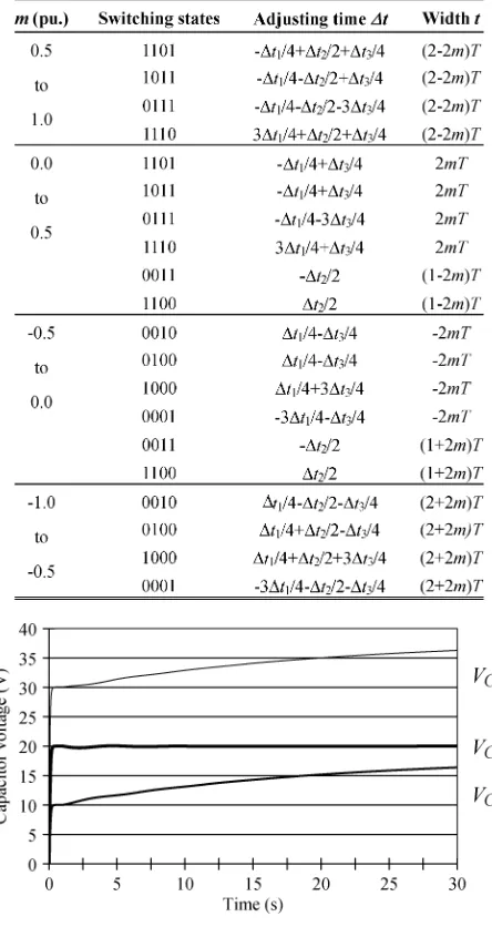
Step 2: The total adjusting time for every selected switching state can be obtained by summing the adjusting times for all capacitors as listed in Table III. According to PS–PWM, the width of each state, i.e., the time duration is a function of
TABLE II
ADJUSTMENT OFSELECTEDSWITCHINGSTATES FORINDIVIDUALCAPACITORS
, which is also listed in Table III. The time duration of a state
after adjustment should not be less than zero, otherwise
the state would not exist any longer and would result in errors
of PWM switching. of a state should also not be larger
than a maximum value which could result in a negative value
of of another state, but if 0 for all states,
has been limited to be less than the maximum value automatically because the overall adjusting time is zero. Thus, only the following condition should be met for all states:
(1)
If , then it must be normalized to the width
(2)
where . Correspondingly, all other adjusting times
also multiply the same coefficient to guarantee the overall
adjusting time in any region being zero.
Step 3: There can be various methods to adjust the time du-ration of selected switching states and determine switching in-stants. The method used in this paper is to adjust states from left to right and to shift only switching instants on the right of a
se-lected state. The region of 0.5 pu. 1.0 pu. is once again
used as an example to illustrate the method of adjusting time
duration of every selected state. For any , , and ,
the adjusting time for all four states in this region can be
calculated by using formulas in Table III. Assuming 0
and 0 to adjust only, the adjusting time
is 4 for the state 1101, 4 for 1011, 4
for 0111, and 3 4 for 1110, respectively. The switching
states before adjustment are obtained using the conventional PS–PWM method as shown in Fig. 4. For the state 1110, since it is distributed at both ends of each cycle, the time duration at
the left end is increased by half of 3 4, i.e., is shifted
right by 3 8. At the same time, all other switching instants
TABLE III
ADJUSTING TIME OF SELECTEDSWITCHING
STATES ANDTHEIRTIMEDURATION
Fig. 5. FC voltages with the conventional PS–PWM method.
, and ) are shifted right by 3 8. For the state 0111,
only its right switching instant, i.e. is shifted left by 4.
At the same time, all other switching instants on the right of
(including , , , , and ) are shifted
left by 4. For the state 1011, only its right switching
in-stant, i.e. is shifted left by 4. At the same time, all
other switching instants on the right of (including ,
, and ) are shifted left by 4. For the state 1101,
is shifted left by 4. At the same time, is shifted
left by 4. After these adjustments, it can be known that the
time duration of 1110 at the right end has actually increased by
3 8, which means the total time duration for 1110 increases
by 3 4 as required. Therefore, new switching instants for all
states after adjustment can be obtained and shown in Fig. 4.
V. SIMULATIONRESULTS
To verify the performance of the voltage balancing control al-gorithm, simulations are carried out on a single-phase five-level
Fig. 6. Phase output voltage v with the conventional PS–PWM method (THD=15.9%).
Fig. 7. Phase output current i with the conventional PS–PWM method (THD=6.7%).
FC converter. Parameters of the converter system are:
40 V, 30 V, 20 V, 10 V, 50 Hz,
1600 Hz, 1500 F; Load: 15 ,
20 mH; PI controller: 10 , 2 10 . Here, is
the fundamental frequency, or modulating frequency, is the
carrier frequency or the switching frequency.
In simulations, from 0 to 1 s, voltages of FCs , , and
are charged to their balance points, i.e., 10, 20, and 30 V respectively through an external charging circuit. After 1 s, the external charging circuit is disconnected and the conventional PS–PWM method starts to work and generates a 50-Hz
sinu-soidal output voltage . The amplitude modulation ratio of is
0.8. Since there is no feedback control, capacitor voltages have deviated from their balance points as shown in Fig. 5.
Espe-cially and have increased to 17 V and 37 V. The output
voltage and output current have deteriorated, as shown in
Figs. 6 and 7. After 30 s, the modified PS–PWM method starts to operate, and capacitor voltages are controlled back to their
bal-ance points, as shown in Fig. 8. Waveforms of and shown
in Figs. 9 and 10 are thus significantly improved. The total
har-monic distortion (THD) of decreases from 15.9% to 13.1%
and the THD of decreases from 6.7% to 5.3%.
VI. EXPERIMENTALRESULTS
Fig. 8. FC voltages with the modified PS–PWM method.
Fig. 9. Phase output voltage v with the modified PS–PWM method (THD=13.1%).
Fig. 10. Phase output current i with the modified PS–PWM method (THD=5.3%).
used in order to provide the control solution. The parameters of the converter prototype, load conditions and controllers are the same as those used in simulations.
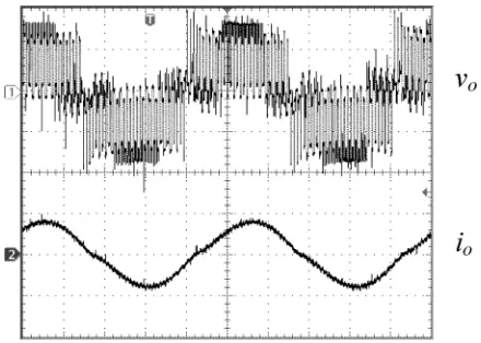
Fig. 11 shows the voltage waveforms of the three FCs before and after the modified PS–PWM control method takes action. In the captured oscilloscope window, the conventional PS–PWM method operates until 20 s, and the voltage imbalance can be observed. The capacitor voltages have deviated to 16, 20.5, and 36 V, respectively from their balance points. From 20 s the modified PS–PWM method starts to operate, and the capacitor voltages are controlled back to balance points. Figs. 12 and 13 give the waveforms of the output voltage and current with the PS–PWM method and with the modified PS–PWM method, re-spectively, for a comparison. The waveform quality has been improved with the modified PS–PWM method.
Fig. 11. FC voltages with the conventional PS–PWM method before 20 s and with the modified PS–PWM method after 20 s. Scales of oscilloscope: 10 V/div and 10 s/div.
Fig. 12. Output voltage and current with the conventional PS–PWM method. Ch1:v (10 V/div); Ch2:i (1 A/div); time (4 ms/div).
Fig. 13. Output voltage and current with the modified PS–PWM method. Ch1:
v (10 V/div); Ch2:i (1 A/div); time (4 ms/div).
VII. CONCLUSION
instants of PS–PWM so as to compensate for the deviation of the capacitor voltages. The proposed method can maintain bal-anced voltages of FCs, which contributes to both the quality of the output voltages and safe operation of the converter. In sum-mary, the method has the following features.
• The overall adjusting time is zero in each switching period in order to keep the duty cycle unchanged. Therefore, the output voltage performance is not affected by such an ad-justment.
• Each capacitor voltage is adjusted individually and their control is decoupled.
• This method can be extended to higher-level FC converters and can be easily implemented with a typical DSP con-troller.
REFERENCES
[1] J. S. Lai and F. Z. Peng, “Multilevel converters-a new breed of power converters,”IEEE Trans. Ind. Appl., vol. 32, no. 3, pp. 509–517, May/ Jun. 1996.
[2] J. Rodriguez, J. S. Lai, and F. Z. Peng, “Multilevel inverters: a survey of topologies, controls, and applications,”IEEE Trans. Ind. Electron., vol. 49, no. 4, pp. 724–738, Aug. 2002.
[3] L. M. Tolbert, F. Z. Peng, and T. G. Habetler, “Multilevel converters for large electric drives,”IEEE Trans. Ind. Appl., vol. 35, no. 1, pp. 36–44, Jan./Feb. 1999.
[4] A. Nabae, I. Takahashi, and H. Akagi, “A new neutral-point-clamped PWM inverter,”IEEE Trans. Ind. Appl., vol. IA-17, no. 5, pp. 518–523, Sep./Oct. 1981.
[5] T. A. Meynard and H. Foch, “Multi-level choppers for high voltage applications,”Eur. Power Electron. Drives J., vol. 2, no. 1, pp. 45–50, 1992.
[6] F. Z. Peng, J. S. Lai, J. W. McKeever, and J. VanCoevering, “A mul-tilevel voltage-source inverter with separate dc sources for static VAr generation,”IEEE Trans. Ind. Appl., vol. 32, no. 5, pp. 1130–1138, Sep./Oct. 1996.
[7] X. Yuan, H. Stemmler, and I. Barbi, “Investigation on the clamping voltage self-balancing of the three-level capacitor clamping in-verter,” inProc. IEEE Power Electron. Spec. Conf., 1999, vol. 2, pp. 1059–1064.
[8] S. G. Lee, D. W. Kang, Y. H. Lee, and D. S. Hyun, “The carrier-based PWM method for voltage balance of flying capacitor multilevel in-verter,” inProc. IEEE Power Electron. Spec. Conf., Vancouver, BC, Canada, Jun. 17–21, 2001, vol. 1, pp. 126–131.
[9] B. M. Song, J. Kim, J. S. Lai, K. C. Seong, H. J. Kim, and S. S. Park, “A multilevel soft-switching inverter with inductor coupling,”IEEE Trans. Ind. Appl., vol. 37, no. 2, pp. 628–636, Mar./Apr. 2001.
[10] M. F. Escalante, J. C. Vannier, and A. Arzande, “Flying capacitor mul-tilevel inverters and DTC motor drive applications,”IEEE Trans. Ind. Electron., vol. 49, no. 4, pp. 809–815, Aug. 2002.
[11] D. W. Kang, W. K. Lee, and D. S. Hyun, “Carrier-rotation strategy for voltage balancing in flying capacitor multilevel inverter,”Proc. Inst. Elect. Eng., vol. 151, no. 2, pp. 239–248, 2004.
[12] G. Gateau, M. Fadel, P. Maussion, R. Bensaid, and T. A. Meynard, “Multicell converters: active control and observation of flying-capac-itor voltages,”IEEE Trans. Ind. Electron., vol. 49, no. 5, pp. 998–1008, Oct. 2002.
[13] T. A. Meynard, M. Fadel, and N. Aouda, “Modeling of multilevel con-verters,”IEEE Trans. Ind. Electron., vol. 44, no. 3, pp. 356–364, Jun. 1997.
[14] J. P. Lavieville, O. Bethoux, P. Carrere, and T. A. Meynard, “Electronic Circuit for Converting Electrical Energy,” U.S. Patent 57 268 70, 1998. [15] J. P. Lavieville and J. Gonzalez, “Multilevel Power Converter With Self-Correction Capacitor Charge Timing Adjustment,” U.S. Patent 58 285 61, 1998.
[16] L. Xu and V. G. Agelidis, “Active capacitor voltage control of flying capacitor multilevel converters,”Proc. Inst. Elect. Eng., vol. 151, no. 3, pp. 313–320, May 2004.
[17] B. M. Song, J. S. Lai, C. Y. Jeong, and D. W. Yoo, “A soft-switching high-voltage active power filter with flying capacitors for urban Maglev system applications,” inProc. IEEE/IAS Annu. Meeting, Chicago, IL, 2001, vol. 3, pp. 1461–1468.
[18] J. Holtz, W. Lotzkat, and K. H. Werner, “A high-power multitran-sistor-inverter uninterruptible power supply system,” IEEE Trans. Power Electron., vol. PE-3, no. 3, pp. 278–285, May 1988.
Chunmei Feng(S’03–M’06) received the B.S. and the M.S. degrees in electrical engineering from Huazhong University of Science and Technology, Wuhan, China, in 1992 and 1996, respectively, and the PhD degree in power electronics from the University of Glasgow, Glasgow, U.K., in 2004.
From 1996 to 2001, she was a lecturer at Tsinghua University, Beijing, China. Currently, she is a Re-search Associate in the Department of Electrical and Electronic Engineering, Imperial College London, U.K. Her research interest includes multilevel con-verters, advanced control applied to the power electronics, distribution systems, electromagnetic measurement, and instrumentation.
Jun Liang(M’02) received the B.S. degree in elec-trical engineering from Huazhong University of Sci-ence and Technology, Wuhan, China, in 1992 and the M.S. and Ph.D. degrees in electrical engineering from the China Electric Power Research Institute (CEPRI), Beijing, in 1995 and 1998, respectively.
From 1998 to 2001, he was a Senior Engineer with CEPRI. From 2001 to 2005, he was a Research Associate in the Department of Electrical and Electronic Engineering, Imperial College London, London, U.K. He is currently a Senior Lecturer in the School of Electronics, University of Glamorgan, Glamorgan, U.K. His research interests are power electronics, power system control, renewable power generation, and distributed generation.
Vassilios G. Agelidis(SM’00) was born in Serres, Greece. He received the B.S. degree in electrical engineering from Democritus University of Thrace, Thrace, Greece, in 1988, the M.S. degree in applied science from Concordia University, Montreal, QC, Canada, in 1992, and the Ph.D. degree in electrical engineering from the Curtin University of Tech-nology, Perth, Australia, in 1997.
From 1993 to 1999, was with the School of Elec-trical and Computer Engineering, Curtin University of Technology. In 2000, he joined the University of Glasgow, Glasgow, U.K., as a Research Manager for the Centre for Economic Renewable Power Delivery. In addition, he has authored/coauthored several journal and conference papers as well as Power Electronic Control in Electrical Systems (2002). In January 2005, he was appointed as the inaugural Chair of Power Engineering in the School of Electrical, Energy and Process Engineering, Murdoch University, Perth, Australia.