www.adv-radio-sci.net/5/279/2007/ © Author(s) 2007. This work is licensed under a Creative Commons License.
Advances in
Radio Science
Power supply network design: a case study driven approach
M. Eireiner1, S. Henzler2, T. Missal1, J. Berthold2, and D. Schmitt-Landsiedel11Institute for Technical Electronics, Technical University Munich, Germany 2Infineon Technologies AG, Munich, Germany
Abstract. A study, based on product related scenarios, on power supply integrity issues is conducted. The effective-ness of specific design parameters depends strongly on the expected loading of the power distribution grid. Therefore, the commonly used approach to only use an even current dis-tribution can lead to non-optimal power grid designs. For power grid optimization, a problem reduction from quadratic to linear order is presented. Simulations in a System-on-Chip (SoC) environment show, that power supply integrity mainly depends on the placing of the cores within the SoC die.
1 Introduction
With decreasing feature sizes, power supply integrity has be-come a serious concern in integrated circuit design. Lowered supply voltages, increasing current densities, increasing op-erating frequencies, and increasing sheet resistances have de-creased the noise margins for every process technology. This trend is expected to continue with technology scaling (Nassif and Fakhouri, 2002, Larsson, 1999, Mezhiba and Friedman, 2004).
Up to now, the design of power distribution networks has been the only design method to combat power supply distor-tions. The design of a power distribution grids includes the choice of how many of the available metal layers are used for power distribution, as well as the sizing, in terms of widths and pitches, of the used metal layers. The thickness of a metal layer is given by technology and therefore is no design parameter.
The rest of the paper is organized as follows. In Sect. 2 and Sect. 3 the movitation and the simulation setup are outlined. Simulation results for single parameter sweeps are presented in Sect. 4, for combined parameter sweeps in Sect. 5. A SoC environment is analyzed in Sect. 6.
Correspondence to: M. Eireiner ([email protected])
2 Motivation
Based on the International Technology Roadmap for Semi-conductors (ITRS) (ITRS, 2005), for technology nodes from 130 nm to 45 nm, values for sheet resistance (R) of local and intermediate signal wires, supply voltage (VDD), power
density (P/A), current density (I/A), and the resulting IR-Drop are displayed in Table 1. All values are normalized to their corresponding value in the 90 nm technology node. We see that from the 90nm to the 45nm technology, the sheet resistance will increase by a factor of 2.07 and 1.77 for lo-cal and intermediate signal wires, respectively. The current density will also increase by a factor of 1.46. This together results in an IR-Drop increase of about a factor of 2.6–3.0 de-pending on the usage of local and intermediate signal wires for supply voltage delivery.
Therefore, power supply integrity is a growing concern not only for high performance, but also for low power designs.
Another point which increases the challenge of power sup-ply network design is that the power supsup-ply network has to be designed at an early stage in the design process. There-fore, only little is know about the actual power distribution within the chip (Benoit et al., 1998). Since after the rout-ing the power grid hardly can be changed, it is a common approach to estimate the power consumption of a chip, mul-tiply it by a factor of three to seven, depending on the circuit architecture and on how conservative the chip is designed, and distribute it evenly over the entire chip based on a DC simulation (Dharchoudhury et al., 1998). For these reasons, power distribution grids are always designed over conserva-tive. Therefore, up to one third of the available metal re-sources in one layer might be used for power distribution. A DC simulation is much faster compared to a transient simulation. However, this comes at the cost that transient ef-fects are lost in the simulation setup. In (Saint-Laurent and Swaminathan, 2004) it was shown that the cycle average of the supply voltage can be taken as key metric for path delay degradation. To verify this, we did simulations on a criti-cal path replica in a 90 nm technology. The nominal sup-ply voltage is 1.2 V. In Fig. 1 the resulting path delay versus the cycle average of the variation of effective supply voltage
280 M. Eireiner et al.: Power supply network design
Table 1. Scaling properties of IR-Drop normalized to 90 nm
tech-nology node (ITRS, 2005).
130 nm 90 nm 65 nm 45 nm
R(local) 0.7 1 1.54 2.07 (intermed.) 0.85 1 1.44 1.77
VDD 1.13 1 1 0.9
P/A 0.87 1 1.14 1.31
I/A 0.77 1 1.14 1.46
IR-Drop 0.54–0.65 1 1.64–1.76 2.58–3.02
2
M. Eireiner, et al: Power Supply Network Design
architecture and on how conservative the chip is designed,
and distribute it evenly over the entire chip based on a DC
simulation [Dharchoudhury et al. (1998)]. For these reasons,
power distribution grids are always designed over
conserva-tive. Therefore, up to one third of the available metal
re-sources in one layer might be used for power distribution.
A DC simulation is much faster compared to a transient
sim-ulation. However, this comes at the cost that transient
ef-fects are lost in the simulation setup. In [Saint-Laurent and
Swaminathan (2004)] it was shown that the cycle average of
the supply voltage can be taken as key metric for path delay
degradation. To verify this, we did simulations on a critical
path replica in a 90nm technology. The nominal supply
volt-age is 1.2V. In Fig. 1 the resulting path delay versus the cycle
average of the variation of effective supply voltage
∆
V
Supplyis displayed. Here, the effective supply voltage
V
Supplyis
defined as the difference between the cycle average of
V
DDand
V
SS, respectively. In turn
∆
V
Supplyis defined as the
difference between the case of no noise, 1.2V, and the noisy
one:
∆
V
Supply= 1
.
2
V
−
V
Supply noise. The graphs with
the circles and rectangular symbols are simulation sweeps, in
which
V
DDand
V
SS, respectively, are kept constant during
one simulation run. Both graphs act as reference. The solid
black lines give a 5% boundary around the
V
SSsweep. The
graphs with crosses and stars show the results of simulations
with transient varying
V
SScurves. Sinodial and rectangular
curves were taken with varying amplitude and/or frequency.
The frequency range for the sinodial noise was swept from
100MHz up to 40GHz. However, most of the simulation
re-sults, which had almost perfect correlation with the reference
simulation are not shown due to reasons of clarity. The peak
to peak amplitude of the ground disturbance was up to 0.6V.
We see that all simulations, with one minor exception, show
an error which is well below 5%. Simulations with transient
varying
V
DDcurves showed similar results. Therefore, the
exact waveform of
V
DDand
V
SSare not of concern but only
their cycle average has to be taken into consideration if the
effect of power supply distortions on path delay variations is
analyzed.
Hence, fast DC simulations instead of expensive transient
simulations were performed to allow for a fast evaluation of
varying power grid sizings.
3
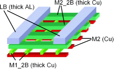
Simulation Setup
We base our analysis on the example of an ARM926 core
in a 90nm technology, as it is described in [Lueftner et al.
(2006)]. As initial point of our analysis we take a power
distribution grid, which consists of four layers.
The top
layer, LB, is a thick aluminum layer, followed by two
cop-per metal layers with double height for intermediate signal
wiring, M2 2B and M1 2B, and finally the local power rails
in the M2 layer, which is a copper layer with single height.
The layers are orthogonal to each other and are connected
frequent with vias at the crossing points. The schematic is
depicted in Fig. 2. For our analysis we take a symmetric
−0.1 −0.075 −0.05 −0.025 0 0.025 0.05 0.075 0.1 1.05 1.1 1.15 1.2 1.25 1.3 1.35 1.4 1.45 1.5
Cycle Average ∆V
Supply
Path Delay [ns]
V
SS DC Ref
V
DD DC Ref
V
SS sine sweep
V
SS rect sweep
V
SS sine 0.1GHz
VSS sine 0.9GHz VSS sine 2GHz VSS sine 5GHz VSS sine 10GHz VSS sine 40GHz
Fig. 1. Path delay versus cycle average of effective supply voltage
VSupply for varying VSS/VDD curves, with amplitudes +/- 0.3V. The solid black lines give a 5% boundary around theVSSreference case.
600
µm
×
1200
µm
section of the power grid. The end points
of the layers at the section boundary are short-circuited with
their starting points to supress artefacts. From the power data
Fig. 2. Schematic of the used 4 stages power grid.
given in [Lueftner et al. (2006)] the average power
consump-tion was taken and multiplied by a factor of three for
tempo-ral variations. For latetempo-ral variations of the grid loading, two
different settings were analyzed. In the first loading scenario
the power is distributed evenly across the whole chip. In the
second scenario, a hotspot was created in the middle of the
power grid. The hotspot is
150
µm
×
300
µm
and has a
cur-rent density which is three times higher than in the case of
the even loading, the schematic is depicted in Fig. 3. The
current density in the rest of the chip was chosen such that
for Even and Hotspot loading the same total current density
resulted.
4
Single Parameter Sweeps
In the first analysis all design parameter of the power grid are
varied one at the time, with the others at their initial value,
and the resulting IR-Drop was simulated for both loading
scenarios. The pitch of the lowest power rail is given through
Fig. 1. Path delay versus cycle average of effective supply voltage VSupply for varyingVSS/VDD curves, with amplitudes +/–0.3 V.
The solid black lines give a 5% boundary around theVSSreference
case.
1VSupply is displayed. Here, the effective supply voltage VSupplyis defined as the difference between the cycle average ofVDDandVSS, respectively. In turn1VSupplyis defined as the difference between the case of no noise, 1.2 V, and the noisy one: 1VSupply=1.2 V−VSupply noise. The graphs with the circles and rectangular symbols are simulation sweeps, in whichVDDandVSS, respectively, are kept constant during
one simulation run. Both graphs act as reference. The solid black lines give a 5% boundary around theVSSsweep. The
graphs with crosses and stars show the results of simulations with transient varyingVSScurves. Sinodial and rectangular
curves were taken with varying amplitude and/or frequency. The frequency range for the sinodial noise was swept from 100 MHz up to 40 GHz. However, most of the simulation re-sults, which had almost perfect correlation with the reference simulation are not shown due to reasons of clarity. The peak to peak amplitude of the ground disturbance was up to 0.6 V. We see that all simulations, with one minor exception, show an error which is well below 5%. Simulations with transient varyingVDD curves showed similar results. Therefore, the
architecture and on how conservative the chip is designed, and distribute it evenly over the entire chip based on a DC simulation [Dharchoudhury et al. (1998)]. For these reasons, power distribution grids are always designed over conserva-tive. Therefore, up to one third of the available metal re-sources in one layer might be used for power distribution. A DC simulation is much faster compared to a transient sim-ulation. However, this comes at the cost that transient ef-fects are lost in the simulation setup. In [Saint-Laurent and Swaminathan (2004)] it was shown that the cycle average of the supply voltage can be taken as key metric for path delay degradation. To verify this, we did simulations on a critical path replica in a 90nm technology. The nominal supply volt-age is 1.2V. In Fig. 1 the resulting path delay versus the cycle average of the variation of effective supply voltage∆VSupply
is displayed. Here, the effective supply voltageVSupply is
defined as the difference between the cycle average ofVDD
and VSS, respectively. In turn ∆VSupply is defined as the
difference between the case of no noise, 1.2V, and the noisy one: ∆VSupply = 1.2V −VSupply noise. The graphs with
the circles and rectangular symbols are simulation sweeps, in whichVDD andVSS, respectively, are kept constant during
one simulation run. Both graphs act as reference. The solid black lines give a 5% boundary around theVSS sweep. The
graphs with crosses and stars show the results of simulations with transient varyingVSScurves. Sinodial and rectangular
curves were taken with varying amplitude and/or frequency. The frequency range for the sinodial noise was swept from 100MHz up to 40GHz. However, most of the simulation re-sults, which had almost perfect correlation with the reference simulation are not shown due to reasons of clarity. The peak to peak amplitude of the ground disturbance was up to 0.6V. We see that all simulations, with one minor exception, show an error which is well below 5%. Simulations with transient varyingVDD curves showed similar results. Therefore, the
exact waveform ofVDDandVSSare not of concern but only
their cycle average has to be taken into consideration if the effect of power supply distortions on path delay variations is analyzed.
Hence, fast DC simulations instead of expensive transient simulations were performed to allow for a fast evaluation of varying power grid sizings.
3 Simulation Setup
We base our analysis on the example of an ARM926 core in a 90nm technology, as it is described in [Lueftner et al. (2006)]. As initial point of our analysis we take a power distribution grid, which consists of four layers. The top layer, LB, is a thick aluminum layer, followed by two cop-per metal layers with double height for intermediate signal wiring, M2 2B and M1 2B, and finally the local power rails in the M2 layer, which is a copper layer with single height. The layers are orthogonal to each other and are connected frequent with vias at the crossing points. The schematic is depicted in Fig. 2. For our analysis we take a symmetric
−0.1 −0.075 −0.05 −0.025 0 0.025 0.05 0.075 0.1 1.05 1.1 1.15 1.2 1.25 1.3 1.35 1.4 1.45 1.5
Cycle Average ∆V
Supply
Path Delay [ns]
VSS DC Ref V
DD DC Ref
VSS sine sweep V
SS rect sweep
VSS sine 0.1GHz V
SS sine 0.9GHz
V
SS sine 2GHz
V
SS sine 5GHz
V
SS sine 10GHz
V
SS sine 40GHz
Fig. 1. Path delay versus cycle average of effective supply voltage VSupply for varyingVSS/VDDcurves, with amplitudes +/- 0.3V. The solid black lines give a 5% boundary around theVSSreference case.
600µm×1200µmsection of the power grid. The end points of the layers at the section boundary are short-circuited with their starting points to supress artefacts. From the power data
Fig. 2. Schematic of the used 4 stages power grid.
given in [Lueftner et al. (2006)] the average power consump-tion was taken and multiplied by a factor of three for tempo-ral variations. For latetempo-ral variations of the grid loading, two different settings were analyzed. In the first loading scenario the power is distributed evenly across the whole chip. In the second scenario, a hotspot was created in the middle of the power grid. The hotspot is150µm×300µmand has a cur-rent density which is three times higher than in the case of the even loading, the schematic is depicted in Fig. 3. The current density in the rest of the chip was chosen such that for Even and Hotspot loading the same total current density resulted.
4 Single Parameter Sweeps
In the first analysis all design parameter of the power grid are varied one at the time, with the others at their initial value, and the resulting IR-Drop was simulated for both loading scenarios. The pitch of the lowest power rail is given through
Fig. 2. Schematic of the used 4 stages power grid.
exact waveform ofVDDandVSSare not of concern but only
their cycle average has to be taken into consideration if the effect of power supply distortions on path delay variations is analyzed. Hence, fast DC simulations instead of expen-sive transient simulations were performed to allow for a fast evaluation of varying power grid sizings.
3 Simulation setup
We base our analysis on the example of an ARM926 core in a 90nm technology, as it is described in (Lueftner et al., 2006). As initial point of our analysis we take a power distri-bution grid, which consists of four layers. The top layer, LB, is a thick aluminum layer, followed by two copper metal lay-ers with double height for intermediate signal wiring, M2 2B and M1 2B, and finally the local power rails in the M2 layer, which is a copper layer with single height. The layers are or-thogonal to each other and are connected frequent with vias at the crossing points. The schematic is depicted in Fig. 2. For our analysis we take a symmetric 600µm×1200µm tion of the power grid. The end points of the layers at the sec-tion boundary are short-circuited with their starting points to supress artefacts.
From the power data given in (Lueftner et al., 2006) the average power consumption was taken and multiplied by a factor of three for temporal variations. For lateral varia-tions of the grid loading, two different settings were ana-lyzed. In the first loading scenario the power is distributed evenly across the whole chip. In the second scenario, a hotspot was created in the middle of the power grid. The hotspot is 150µm×300µm and has a current density which is three times higher than in the case of the even loading, the schematic is depicted in Fig. 3. The current density in the rest of the chip was chosen such that for Even and Hotspot loading the same total current density resulted.
M. Eireiner et al.: Power supply network design 281 M. Eireiner, et al: Power Supply Network Design 3
Fig. 3. Schematic of the hotspot loading. A hotspot, 150µm× 300µm, with a three times higher current density compared to the even case is placed in the middle of the power grid. The remaining power grid was loaded such that the overall current density matched for Hotspot and Even loading
the height of a standard cell. The pitch of the LB layer is set through minimum bump pitch requirements. Therefore, six independent design parameters, four width and two pitch pa-rameters, exist.
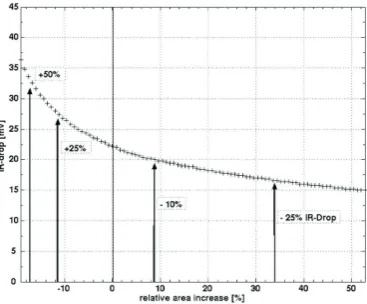
For every design parameter a sweep across a wide parameter range was conducted. The increase or decrease of a design parameter was translated into an equivalent relative increase or decrease in area. The resulting IR-Drop depending on the change in area is displayed in Fig. 4, here at the example of varying M2 width with Hotspot loading. The resulting
Fig. 4. Resulting IR-Drop for varying M2 width for the Hotspot
loading. An increase/decrease of M2 width is translated into a rela-tive increase/decrease of area
graphs for the remaining five design parameters look simi-lar to the one for the M2 width sweep in Fig. 4. Changing from Hotspot to Even loading results in a decrease of IR-Drop by preserving roughly the shape of the graph. However, it has to be mentioned that in our use case, in which the grid is connected by bumps to the package supply every600µm see Fig. 2, virtually no voltage drop occurs in the LB layer.
Therefore, changing the width of the LB layer has minimal impact on the resulting IR-Drop.
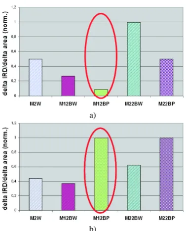
Based on the simulations described above, a cost perfor-mance analysis in terms of resulting change in IR-Drop and change in occupied area is conducted for both loading sce-narios. Fig. 5 shows the effectiveness of a design change for the different design parameters. Effectiveness is defined as ∆IR∆rel.area−Drop. The effectiveness is derived from the crite-rion how much area is needed to achieve a given reduction in IR-Drop. The less area needed, the more efficient the design parameter is. The results in Fig. 5 are normalized to the max-imum effectiveness in one loading scenario. The LB layer is omitted in this plot, since, as mentioned before, it does not contribute significantly to IR-Drop.
We see that for different loading scenarios of the power grid, the effectiveness of the design parameter drastically changes. For example for Even loading M1 2B pitch has the lowest effectiveness, whereas for a Hotspot loading the situation is vice versa, M1 2B pitch is the preferable parameter to reduce IR-Drop area efficient.
The loading of an actual design hardly will be an Even load-ing, and the critical case for IR-Drop is some hotspot on the chip. Therefore, we see that the common approach to use Even loading for initial power grid dimensioning gives wrong design incentives. This can lead to non-optimal power grid designs in terms of area efficiency. Therefore, we pro-pose to use not only Even loading, but also some Hotspot loading for initial power grid design. With the additional loading scenario effects of lateral varying current densities on power grid dimensioning can be accounted for. Hence, right from the start a better power grid design is possible, which helps to achieve the area efficient optimum.
5 Combined Parameter Sweeps
Power grid design usually is not done by only varying one de-sign parameter, but multiple at a time. The question we want to address in this section is, whether it is possible to estimate the resulting IR-Drop of varying two design paramters at the same time, by taking the simulation results of their single pa-rameter sweeps. Therefore, it would be possible to achieve a problem reduction from a quadratic order,O(N2), to
lin-ear order,O(N). This in turn decreases the simulation time signficantly.
First we tried to estimate the resulting IR-Drop with the ad-ditive equation:
IRDest(v1+ ∆v1, v2+ ∆v2) =IRDsingle(v1+ ∆v1)
+IRDsingle(v2+ ∆)−IRDstd
WhereIRDest(v1+∆v1, v2+∆v2)is the estimated IR-Drop
for changing design paramtersv1andv2,∆IRDsingle(v1+ ∆v1) and ∆IRDsingle(v2 + ∆v2) are the changes in
IR-Drop caused by single design paramter variation ∆v1 and ∆v2, respectively, IRDstdis the IR-Drop for the initial or
standard dimensioning of the power grid. As reference all
Fig. 3. Schematic of the hotspot loading. A hotspot, 150µm×300µm, with a three times higher current density com-pared to the even case is placed in the middle of the power grid. The remaining power grid was loaded such that the overall current density matched for Hotspot and Even loading.
4 Single parameter sweeps
In the first analysis all design parameter of the power grid are varied one at the time, with the others at their initial value, and the resulting IR-Drop was simulated for both loading scenarios. The pitch of the lowest power rail is given through the height of a standard cell. The pitch of the LB layer is set through minimum bump pitch requirements. Therefore, six independent design parameters, four width and two pitch pa-rameters, exist.
For every design parameter a sweep across a wide parame-ter range was conducted. The increase or decrease of a design parameter was translated into an equivalent relative increase or decrease in area. The resulting IR-Drop depending on the change in area is displayed in Fig. 4, here at the example of varying M2 width with Hotspot loading. The resulting graphs for the remaining five design parameters look simi-lar to the one for the M2 width sweep in Fig. 4. Changing from Hotspot to Even loading results in a decrease of IR-Drop by preserving roughly the shape of the graph. However, it has to be mentioned that in our use case, in which the grid is connected by bumps to the package supply every 600µm see Fig. 2, virtually no voltage drop occurs in the LB layer. Therefore, changing the width of the LB layer has minimal impact on the resulting IR-Drop.
Based on the simulations described above, a cost perfor-mance analysis in terms of resulting change in IR-Drop and change in occupied area is conducted for both loading sce-narios. Fig. 5 shows the effectiveness of a design change for the different design parameters. Effectiveness is defined as 11IRrel−.areaDrop. The effectiveness is derived from the criterion how much area is needed to achieve a given reduction in
IR-Fig. 3. Schematic of the hotspot loading. A hotspot, 150µm×
300µm, with a three times higher current density compared to the even case is placed in the middle of the power grid. The remaining power grid was loaded such that the overall current density matched for Hotspot and Even loading
the height of a standard cell. The pitch of the LB layer is set through minimum bump pitch requirements. Therefore, six independent design parameters, four width and two pitch pa-rameters, exist.
For every design parameter a sweep across a wide parameter range was conducted. The increase or decrease of a design parameter was translated into an equivalent relative increase or decrease in area. The resulting IR-Drop depending on the change in area is displayed in Fig. 4, here at the example of varying M2 width with Hotspot loading. The resulting
Fig. 4. Resulting IR-Drop for varying M2 width for the Hotspot
loading. An increase/decrease of M2 width is translated into a rela-tive increase/decrease of area
graphs for the remaining five design parameters look simi-lar to the one for the M2 width sweep in Fig. 4. Changing from Hotspot to Even loading results in a decrease of IR-Drop by preserving roughly the shape of the graph. However, it has to be mentioned that in our use case, in which the grid is connected by bumps to the package supply every600µm
see Fig. 2, virtually no voltage drop occurs in the LB layer.
Therefore, changing the width of the LB layer has minimal impact on the resulting IR-Drop.
Based on the simulations described above, a cost perfor-mance analysis in terms of resulting change in IR-Drop and change in occupied area is conducted for both loading sce-narios. Fig. 5 shows the effectiveness of a design change for the different design parameters. Effectiveness is defined as ∆IR∆rel.area−Drop. The effectiveness is derived from the crite-rion how much area is needed to achieve a given reduction in IR-Drop. The less area needed, the more efficient the design parameter is. The results in Fig. 5 are normalized to the max-imum effectiveness in one loading scenario. The LB layer is omitted in this plot, since, as mentioned before, it does not contribute significantly to IR-Drop.
We see that for different loading scenarios of the power grid, the effectiveness of the design parameter drastically changes. For example for Even loading M1 2B pitch has the lowest effectiveness, whereas for a Hotspot loading the situation is vice versa, M1 2B pitch is the preferable parameter to reduce IR-Drop area efficient.
The loading of an actual design hardly will be an Even load-ing, and the critical case for IR-Drop is some hotspot on the chip. Therefore, we see that the common approach to use Even loading for initial power grid dimensioning gives wrong design incentives. This can lead to non-optimal power grid designs in terms of area efficiency. Therefore, we pro-pose to use not only Even loading, but also some Hotspot loading for initial power grid design. With the additional loading scenario effects of lateral varying current densities on power grid dimensioning can be accounted for. Hence, right from the start a better power grid design is possible, which helps to achieve the area efficient optimum.
5 Combined Parameter Sweeps
Power grid design usually is not done by only varying one de-sign parameter, but multiple at a time. The question we want to address in this section is, whether it is possible to estimate the resulting IR-Drop of varying two design paramters at the same time, by taking the simulation results of their single pa-rameter sweeps. Therefore, it would be possible to achieve a problem reduction from a quadratic order,O(N2), to
lin-ear order,O(N). This in turn decreases the simulation time signficantly.
First we tried to estimate the resulting IR-Drop with the ad-ditive equation:
IRDest(v1+ ∆v1, v2+ ∆v2) =IRDsingle(v1+ ∆v1)
+IRDsingle(v2+ ∆)−IRDstd
WhereIRDest(v1+∆v1, v2+∆v2)is the estimated IR-Drop
for changing design paramtersv1andv2,∆IRDsingle(v1+
∆v1)and ∆IRDsingle(v2+ ∆v2)are the changes in
IR-Drop caused by single design paramter variation ∆v1 and
∆v2, respectively,IRDstd is the IR-Drop for the initial or
standard dimensioning of the power grid. As reference all
Fig. 4. Resulting IR-Drop for varying M2 width for the Hotspot
loading. An increase/decrease of M2 width is translated into a rela-tive increase/decrease of area.
Drop. The less area needed, the more efficient the design parameter is. The results in Fig. 5 are normalized to the max-imum effectiveness in one loading scenario. The LB layer is omitted in this plot, since, as mentioned before, it does not contribute significantly to IR-Drop.
We see that for different loading scenarios of the power grid, the effectiveness of the design parameter drastically changes. For example for Even loading M1 2B pitch has the lowest effectiveness, whereas for a Hotspot loading the situ-ation is vice versa, M1 2B pitch is the preferable parameter to reduce IR-Drop area efficient.
The loading of an actual design hardly will be an Even loading, and the critical case for IR-Drop is some hotspot on the chip. Therefore, we see that the common approach to use Even loading for initial power grid dimensioning gives wrong design incentives. This can lead to non-optimal power grid designs in terms of area efficiency. Therefore, we pro-pose to use not only Even loading, but also some Hotspot loading for initial power grid design. With the additional loading scenario effects of lateral varying current densities on power grid dimensioning can be accounted for. Hence, right from the start a better power grid design is possible, which helps to achieve the area efficient optimum.
5 Combined parameter sweeps
Power grid design usually is not done by only varying one design parameter, but multiple at a time. The question we want to address in this section is, whether it is possible to es-timate the resulting IR-Drop of varying two design paramters at the same time, by taking the simulation results of their sin-gle parameter sweeps. Therefore, it would be possible to achieve a problem reduction from a quadratic order,O(N2),
282 M. Eireiner et al.: Power supply network design
4 M. Eireiner, et al: Power Supply Network Design
a)
b)
Fig. 5. Effectiveness in terms of IR-Drop over relative area change
for given reduction in IR-Drop for varying design paramters. a) Even loading b) hotspot loading
combinations of parameter sweeps were simulated. How-ever, the additive IR-Drop estimation showed high deviation from the reference simulation and therefore can not be used for an acurate estimation.
As a second approach we tried to estimate the resulting IR-Drop with the multiplicative equation:
IRDest(v1+ ∆v1, v2 + ∆v2) =
IRDsingle(v1+ ∆v1)·IRDsingle(v2+ ∆v2)
IRDstd
To visualize the normalized error,Errnorm, between the
simulated and the estimated IR-Drop the error was calculated for all parameter cominations:
Errnorm= IRDsim−IRDest
IRDsim
The resulting error map over the entire parameter range, here at the example for varying M1 2B width and M2 2B width, is displayed in Fig. 6. The color of the map reflects the re-sulting error in percentage. In Fig. 7 the histogram for the error map of Fig. 6 is displayed. The error in this case is between -2% and +4%. For all possible combinations of pa-rameter variations over the entire relevant design space the error is in the range of±10%. Therefore, the resulting IR-Drop of changing two design paramters at the same time can efficiently and accurately be estimated by the proposed equa-tion. Hence, a problem reduction from quadratic to linear or-der was achieved.
Up to now, no analytical derivation for the good fit of the
multiplicative approach can be given. But it is expected, that parallel connections of power rails, e.g. LB||M1 2B and M2 2B||M2, are responsible for the malfunction of the addi-tive as well as for the good fit of the multiplicaaddi-tive approach. However, more research has to be done to derive an analyti-cal verification of the observed phenomenon.
Fig. 6. Resulting error map for estimating IR-Drop multiplicatively,
for varying M1 2B width and M2 2B width
Fig. 7. Histogram for the error map of Fig. 6
6 SoC Power Grid Example
As an other example, we consider an System on Chip (SoC) design, as it is presented in [Lueftner et al. (2006)]. We choose a chip size of6mm×6mm. The schematic of an exemplary power distribution is given in Fig. 8. In the green region in the middle of the chip, regular bump connections are available. In the outer pink region no bump connections are available due to package constraints. In the red region at the edge of the chip, the I/O connections are located and therefore, no bump connections for power distribution and no power routing in the LB metal layer is possible.
As loading we again take an ARM926 core, with a die size of
Fig. 5. Effectiveness in terms of IR-Drop over relative area change
for given reduction in IR-Drop for varying design paramters. (a) Even loading (b) hotspot loading
to linear order,O(N ). This in turn decreases the simulation time signficantly.
First we tried to estimate the resulting IR-Drop with the additive equation:
IRDest(v1+1v1, v2+1v2)=IRDsingle(v1+1v1) +IRDsingle(v2+1v2)−IRDstd
Where IRDest(v1+1v1, v2+1v2) is the estimated IR-Drop for changing design paramters v1 and v2, 1IRDsingle(v1+1v1) and 1IRDsingle(v2+1v2) are the changes in IR-Drop caused by single design paramter variation1v1and1v2, respectively,I RDstdis the IR-Drop for the initial or standard dimensioning of the power grid. As reference all combinations of parameter sweeps were simulated. However, the additive IR-Drop estimation showed high deviation from the reference simulation and therefore can not be used for an acurate estimation.
As a second approach we tried to estimate the resulting IR-Drop with the multiplicative equation:
IRDest(v1+1v1, v2+1v2)=
IRDsingle(v1+1v1)·IRDsingle(v2+1v2) IRDstd
To visualize the normalized error, Errnorm, between the simulated and the estimated IR-Drop the error was calculated for all parameter cominations:
Errnorm=
IRDsim−IRDest IRDsim
a)
b)
Fig. 5. Effectiveness in terms of IR-Drop over relative area change
for given reduction in IR-Drop for varying design paramters. a) Even loading b) hotspot loading
combinations of parameter sweeps were simulated. How-ever, the additive IR-Drop estimation showed high deviation from the reference simulation and therefore can not be used for an acurate estimation.
As a second approach we tried to estimate the resulting IR-Drop with the multiplicative equation:
IRDest(v1+ ∆v1, v2 + ∆v2) =
IRDsingle(v1+ ∆v1)·IRDsingle(v2+ ∆v2)
IRDstd
To visualize the normalized error,Errnorm, between the
simulated and the estimated IR-Drop the error was calculated for all parameter cominations:
Errnorm=
IRDsim−IRDest
IRDsim
The resulting error map over the entire parameter range, here at the example for varying M1 2B width and M2 2B width, is displayed in Fig. 6. The color of the map reflects the re-sulting error in percentage. In Fig. 7 the histogram for the error map of Fig. 6 is displayed. The error in this case is between -2% and +4%. For all possible combinations of pa-rameter variations over the entire relevant design space the error is in the range of±10%. Therefore, the resulting IR-Drop of changing two design paramters at the same time can efficiently and accurately be estimated by the proposed equa-tion. Hence, a problem reduction from quadratic to linear or-der was achieved.
Up to now, no analytical derivation for the good fit of the
multiplicative approach can be given. But it is expected, that parallel connections of power rails, e.g. LB||M1 2B and M2 2B||M2, are responsible for the malfunction of the addi-tive as well as for the good fit of the multiplicaaddi-tive approach. However, more research has to be done to derive an analyti-cal verification of the observed phenomenon.
Fig. 6. Resulting error map for estimating IR-Drop multiplicatively,
for varying M1 2B width and M2 2B width
Fig. 7. Histogram for the error map of Fig. 6
6 SoC Power Grid Example
As an other example, we consider an System on Chip (SoC) design, as it is presented in [Lueftner et al. (2006)]. We choose a chip size of6mm×6mm. The schematic of an exemplary power distribution is given in Fig. 8. In the green region in the middle of the chip, regular bump connections are available. In the outer pink region no bump connections are available due to package constraints. In the red region at the edge of the chip, the I/O connections are located and therefore, no bump connections for power distribution and no power routing in the LB metal layer is possible.
As loading we again take an ARM926 core, with a die size of
Fig. 6. Resulting error map for estimating IR-Drop multiplicatively,
for varying M1 2B width and M2 2B width.
The resulting error map over the entire parameter range, here at the example for varying M1 2B width and M2 2B width, is displayed in Fig. 6. The color of the map reflects the re-sulting error in percentage. In Fig. 7 the histogram for the error map of Fig. 6 is displayed. The error in this case is between –2% and +4%. For all possible combinations of pa-rameter variations over the entire relevant design space the error is in the range of±10%. Therefore, the resulting IR-Drop of changing two design paramters at the same time can efficiently and accurately be estimated by the proposed equa-tion. Hence, a problem reduction from quadratic to linear order was achieved.
Up to now, no analytical derivation for the good fit of the multiplicative approach can be given. But it is expected, that parallel connections of power rails, e.g. LB||M1 2B and M2 2B||M2, are responsible for the malfunction of the addi-tive as well as for the good fit of the multiplicaaddi-tive approach. However, more research has to be done to derive an analyti-cal verification of the observed phenomenon.
6 SoC power grid example
As an other example, we consider an System on Chip (SoC) design, as it is presented in (Lueftner et al., 2006). We choose a chip size of 6 mm×6 mm. The schematic of an exemplary power distribution is given in Fig. 8. In the green region in the middle of the chip, regular bump connections are able. In the outer pink region no bump connections are avail-able due to package constraints. In the red region at the edge of the chip, the I/O connections are located and therefore, no bump connections for power distribution and no power rout-ing in the LB metal layer is possible.
As loading we again take an ARM926 core, with a die size of 1 mm×1 mm. The die is placed at varying positions within the SoC and the resulting IR-Drop is simulated. Due
M. Eireiner et al.: Power supply network design 283 a)
b)
Fig. 5. Effectiveness in terms of IR-Drop over relative area change
for given reduction in IR-Drop for varying design paramters. a) Even loading b) hotspot loading
combinations of parameter sweeps were simulated. How-ever, the additive IR-Drop estimation showed high deviation from the reference simulation and therefore can not be used for an acurate estimation.
As a second approach we tried to estimate the resulting IR-Drop with the multiplicative equation:
IRDest(v1+ ∆v1, v2 + ∆v2) =
IRDsingle(v1+ ∆v1)·IRDsingle(v2+ ∆v2)
IRDstd
To visualize the normalized error,Errnorm, between the
simulated and the estimated IR-Drop the error was calculated for all parameter cominations:
Errnorm=
IRDsim−IRDest
IRDsim
The resulting error map over the entire parameter range, here at the example for varying M1 2B width and M2 2B width, is displayed in Fig. 6. The color of the map reflects the re-sulting error in percentage. In Fig. 7 the histogram for the error map of Fig. 6 is displayed. The error in this case is between -2% and +4%. For all possible combinations of pa-rameter variations over the entire relevant design space the error is in the range of±10%. Therefore, the resulting IR-Drop of changing two design paramters at the same time can efficiently and accurately be estimated by the proposed equa-tion. Hence, a problem reduction from quadratic to linear or-der was achieved.
Up to now, no analytical derivation for the good fit of the
multiplicative approach can be given. But it is expected, that parallel connections of power rails, e.g. LB|| M1 2B and M2 2B||M2, are responsible for the malfunction of the addi-tive as well as for the good fit of the multiplicaaddi-tive approach. However, more research has to be done to derive an analyti-cal verification of the observed phenomenon.
Fig. 6. Resulting error map for estimating IR-Drop multiplicatively,
for varying M1 2B width and M2 2B width
Fig. 7. Histogram for the error map of Fig. 6
6 SoC Power Grid Example
As an other example, we consider an System on Chip (SoC) design, as it is presented in [Lueftner et al. (2006)]. We choose a chip size of6mm×6mm. The schematic of an exemplary power distribution is given in Fig. 8. In the green region in the middle of the chip, regular bump connections are available. In the outer pink region no bump connections are available due to package constraints. In the red region at the edge of the chip, the I/O connections are located and therefore, no bump connections for power distribution and no power routing in the LB metal layer is possible.
As loading we again take an ARM926 core, with a die size of
Fig. 7. Histogram for the error map of Fig. 6.
M. Eireiner, et al: Power Supply Network Design 5
1mm×1mm. The die is placed at varying positions within the SoC and the resulting IR-Drop is simulated. Due to rea-sons of symmertry and to reduce simulation time the grid was reduced to the shaded area, 4mm×4mm, in Fig. 8. Exemplarily, three positions of the ARM core within the SoC
Fig. 8. Schematic of the power supply network of an example SoC
with6mm×6mmdie size. ESD and I/O restiction prohibit the bump connections and LB usage in the outer regions of the chip
are depicted in Fig. 9. The resulting maximum, minimum, and average IR-Drop within the core area are tabulated in Tab. 2. For the placing in the lower left corner, almost the entire IR-Drop is on LB and M2 2B layer. M1 2B and M2 contribute only minor to the overall IR-Drop. We see from Tab. 2, that by moving the core only 1mm to the center, max-imum IR-Drop is reduced be about a factor of 10, for mini-mum and average IR-Drop the factors are even higher. Sim-ilar simulations with different placings, e.g. starting in the left center, were also conducted and showed compareable re-sults. Therefore, in a SoC environemnt the placing of the major power consuming cores is the most critical issue for power supply integrity. However, I/O and ESD restrictions might require a placing of such blocks to the edges and I/O pins of the SoC.
Table 2. Power supply noise for varying core positions within SoC
power grid
Low center Half moved moved Max 126.3mV 42.4mV 13.1mV Min 96.7mV 30.1mV 7.2mV Avg 35.9mV 0.2mV 0.2mV
7 Conclusions
In this paper a case study driven approach to power supply integrity analysis was presented. Based on product related
Fig. 9. Schematic of the power supply network of an example SoC
with6mm×6mmdie size. ESD and I/O restiction prohibit the bump connections and LB usage in the outer regions of the chip
scenarios, it was shown that using only the assumption of Even loading for initial power grid design can lead to non-optimal power grids. For the optimization of power grids, it was shown that a problem reduction from quadratic to lin-ear order is possible by using a multiplicative IR-Drop esti-mation. However, an analytical derivation of the used for-mula could not be given and is the goal of future research, as well as the extension from two to multiple design vari-ables. In SoC environments in which I/O, packaging, and ESD requirements restrict the on-chip power routing, almost the entire IR-Drop is in the upper layers. Placing of cores within the SoC has the highest single impact on power sup-ply integrity.
References
Benoit, M., Taylor, S., Overhauser, D., and Rochel, S.: Power Distribution in High-Performance Design, in: Proceedings of IEEE Symposium of Low-Power Electronics Design, pp. 274– 278, 1998.
Dharchoudhury, A., Panda, R., Blaauw, D., and Vaidyanathan, R.: Design and Analysis of Power Distribution Networks in Pow-erPC Mircoprocessors, in: Proceedings of Design Automation Converence, pp. 738–743, 1998.
ITRS: International Technology Roadmap for Semiconductors, http://public.itrs.net/, 2005.
Larsson, P.: Power Supply Noise in Future IC’s: A Crystal Ball Reading, in: IEEE Custom Integrated Circuits Conference, pp. 467–474, 1999.
Lueftner, T., Berthold, J., Pacha, C., Georgakos, G., Sauzon, G., Hoemke, O., Beshenar, J., Mahrla, P., Just, K., Hober, P., Henzler, S., Schmitt-Landsiedel, D., Yakovleff, A., Klein, A., Knight, R., Acharya, P., Mabrouki, H., Juhoor, G., and Sauer, M.: A 90nm CMOS Low-Power GSM/EDGE Multimedia-Enhanced
Fig. 8. Schematic of the power supply network of an example SoC
with 6 mm×6 mm die size. ESD and I/O restiction prohibit the bump connections and LB usage in the outer regions of the chip.
to reasons of symmertry and to reduce simulation time the grid was reduced to the shaded area, 4 mm×4 mm, in Fig. 8. Exemplarily, three positions of the ARM core within the SoC are depicted in Fig. 9. The resulting maximum, minimum, and average IR-Drop within the core area are tabulated in Table 2. For the placing in the lower left corner, almost the entire IR-Drop is on LB and M2 2B layer. M1 2B and M2 contribute only minor to the overall IR-Drop. We see from Table 2, that by moving the core only 1mm to the center, maximum IR-Drop is reduced be about a factor of 10, for minimum and average IR-Drop the factors are even higher. Similar simulations with different placings, e.g. starting in the left center, were also conducted and showed compareable results. Therefore, in a SoC environemnt the placing of the major power consuming cores is the most critical issue for
M. Eireiner, et al: Power Supply Network Design 5
1mm×1mm. The die is placed at varying positions within the SoC and the resulting IR-Drop is simulated. Due to rea-sons of symmertry and to reduce simulation time the grid was reduced to the shaded area, 4mm×4mm, in Fig. 8. Exemplarily, three positions of the ARM core within the SoC
Fig. 8. Schematic of the power supply network of an example SoC
with6mm×6mmdie size. ESD and I/O restiction prohibit the bump connections and LB usage in the outer regions of the chip
are depicted in Fig. 9. The resulting maximum, minimum, and average IR-Drop within the core area are tabulated in Tab. 2. For the placing in the lower left corner, almost the entire IR-Drop is on LB and M2 2B layer. M1 2B and M2 contribute only minor to the overall IR-Drop. We see from Tab. 2, that by moving the core only 1mm to the center, max-imum IR-Drop is reduced be about a factor of 10, for mini-mum and average IR-Drop the factors are even higher. Sim-ilar simulations with different placings, e.g. starting in the left center, were also conducted and showed compareable re-sults. Therefore, in a SoC environemnt the placing of the major power consuming cores is the most critical issue for power supply integrity. However, I/O and ESD restrictions might require a placing of such blocks to the edges and I/O pins of the SoC.
Table 2. Power supply noise for varying core positions within SoC
power grid
Low center Half moved moved Max 126.3mV 42.4mV 13.1mV Min 96.7mV 30.1mV 7.2mV Avg 35.9mV 0.2mV 0.2mV
7 Conclusions
In this paper a case study driven approach to power supply integrity analysis was presented. Based on product related
Fig. 9. Schematic of the power supply network of an example SoC
with6mm×6mmdie size. ESD and I/O restiction prohibit the bump connections and LB usage in the outer regions of the chip
scenarios, it was shown that using only the assumption of Even loading for initial power grid design can lead to non-optimal power grids. For the optimization of power grids, it was shown that a problem reduction from quadratic to lin-ear order is possible by using a multiplicative IR-Drop esti-mation. However, an analytical derivation of the used for-mula could not be given and is the goal of future research, as well as the extension from two to multiple design vari-ables. In SoC environments in which I/O, packaging, and ESD requirements restrict the on-chip power routing, almost the entire IR-Drop is in the upper layers. Placing of cores within the SoC has the highest single impact on power sup-ply integrity.
References
Benoit, M., Taylor, S., Overhauser, D., and Rochel, S.: Power Distribution in High-Performance Design, in: Proceedings of IEEE Symposium of Low-Power Electronics Design, pp. 274– 278, 1998.
Dharchoudhury, A., Panda, R., Blaauw, D., and Vaidyanathan, R.: Design and Analysis of Power Distribution Networks in Pow-erPC Mircoprocessors, in: Proceedings of Design Automation Converence, pp. 738–743, 1998.
ITRS: International Technology Roadmap for Semiconductors, http://public.itrs.net/, 2005.
Larsson, P.: Power Supply Noise in Future IC’s: A Crystal Ball Reading, in: IEEE Custom Integrated Circuits Conference, pp. 467–474, 1999.
Lueftner, T., Berthold, J., Pacha, C., Georgakos, G., Sauzon, G., Hoemke, O., Beshenar, J., Mahrla, P., Just, K., Hober, P., Henzler, S., Schmitt-Landsiedel, D., Yakovleff, A., Klein, A., Knight, R., Acharya, P., Mabrouki, H., Juhoor, G., and Sauer, M.: A 90nm CMOS Low-Power GSM/EDGE Multimedia-Enhanced
Fig. 9. Schematic of the power supply network of an example SoC
with 6 mm×6 mm die size. ESD and I/O restiction prohibit the bump connections and LB usage in the outer regions of the chip.
Table 2. Power supply noise for varying core positions within SoC
power grid.
Low center Half moved Moved
Max 126.3 mV 42.4 mV 13.1 mV Min 96.7 mV 30.1 mV 7.2 mV Avg 35.9 mV 0.2 mV 0.2 mV
power supply integrity. However, I/O and ESD restrictions might require a placing of such blocks to the edges and I/O pins of the SoC.
7 Conclusions
In this paper a case study driven approach to power supply integrity analysis was presented. Based on product related scenarios, it was shown that using only the assumption of Even loading for initial power grid design can lead to non-optimal power grids. For the optimization of power grids, it was shown that a problem reduction from quadratic to lin-ear order is possible by using a multiplicative IR-Drop esti-mation. However, an analytical derivation of the used for-mula could not be given and is the goal of future research, as well as the extension from two to multiple design vari-ables. In SoC environments in which I/O, packaging, and ESD requirements restrict the on-chip power routing, almost the entire IR-Drop is in the upper layers. Placing of cores
within the SoC has the highest single impact on power sup-ply integrity.
References
Benoit, M., Taylor, S., Overhauser, D., and Rochel, S.: Power Dis-tribution in High-Performance Design, in: Proceedings of IEEE Symposium of Low-Power Electronics Design, 274–278, 1998. Dharchoudhury, A., Panda, R., Blaauw, D., and Vaidyanathan, R.:
Design and Analysis of Power Distribution Networks in Pow-erPC Mircoprocessors, in: Proceedings of Design Automation Converence, 738–743, 1998.
ITRS: International Technology Roadmap for Semiconductors, http://public.itrs.net/, 2005.
Larsson, P.: Power Supply Noise in Future IC’s: A Crystal Ball Reading, in: IEEE Custom Integrated Circuits Conference, 467– 474, 1999.
Lueftner, T., Berthold, J., Pacha, C., Georgakos, G., Sauzon, G., Hoemke, O., Beshenar, J., Mahrla, P., Just, K., Hober, P., Henzler, S., Schmitt-Landsiedel, D., Yakovleff, A., Klein, A., Knight, R., Acharya, P., Mabrouki, H., Juhoor, G., and Sauer, M.: A 90 nm CMOS Low-Power GSM/EDGE Multimedia-Enhanced Baseband Processor with 380 MHz ARM9 and Mixed-Signal Ex-tensions, in: 2006 ISSCC Digest of Digital Papers, 252–253, 2006.
Mezhiba, A. V. and Friedman, E. G.: Scaling Trends of On-Chip Power Distribution Noise, IEEE Transactions on Very Large Scale Integration (VLSI) Systems, 12, 386–394, 2004.
Nassif, S. R. and Fakhouri, O.: Technology Trends in Power-Grid-Induced Noise, in: Proceedings of the 2002 international workshop on System-level interconnect prediction, 55–59, ACM Press, 2002.
Saint-Laurent, M. and Swaminathan, M.: Impact of Power-Supply Noise on Timing in High-Frequency Microprocessors, IEEE Transactions on Advanced Packaging, 27, 135–144, 2004.