Copyright © 2013 IJECCE, All right reserved
Design and Simulation of Pipelined FFT Processor Using
FPGA
N. Amarnath Reddy
[email protected].GMR institute of Technology, Rajam, INDIA Email: [email protected]
D. Srinivasa Rao
Asst. Prof, Dept. of ECEGMR institute of Technology, Rajam, INDIA Email: [email protected]
Abstract – A parallel and pipelined Fast Fourier Transform (FFT) processor for use in the Orthogonal Frequency division Multiplexer (OFDM). Unlike being stored in the traditional ROM, the twiddle factors in our pipelined FFT processor can be accessed directly. A novel simple address mapping scheme and the modified radix 4 FFT also proposed. Finally, the pipelined 64-point FFT processor can be completely implemented within 20.093ns.
Keywords–OFDM, FFT, DIF, Radix- 4, FPGA.
I. I
NTRODUCTIONActive radar systems are commonly used in military and commercial applications for the detection and tracking of objects through a medium such as air. Most active radar systems work by transmitting a signal pulse through the medium and receiving the reflected energy wave field as it scatters off objects in the medium. By processing the received wave field, an active radar system can determine an object's distance, velocity, and other features. A passive radar system can consist solely of an array of receiving antennas as opposed to an active radar system with a co-located transmitter and receiver.
Without a transmitter the passive radar system relies on other sources of electromagnetic waves, such as AM or FM radio waves, TV broadcast, nearby radar, cell towers, or a
wideband waveform to “illuminate” objects in the medium.
Various signal processing algorithms can be applied to the data from the antenna array. One algorithm of interest is the Direction of Arrival (DOA) of the incoming scattered waveform and therefore the object. A computationally efficient version of the DFT is known as the Fast Fourier Transform (FFT) and is commonly used to reduce the computational burden.
In the communication world of today more and more OFDM systems are brought on-line with an ever increasing number of standards, applications, and services, all with different requirements on the physical layer of the transceiver. The physical layer is most often, due to speed and power constraints, implemented as an ASIC and thus locked to one specific case. Hence, the number of required implementations will grow fast. Due to this fact, there will
be an interest from the industry’s point of view to search
for a flexible architecture that can be configured to function with several standards, applications, or services. A flexible architecture will lead to re-usage of design and implementation and thus reduced cost. This project addresses both OFDM in theory and the implementation aspects of a flexible hardware solution for digital baseband OFDM[8].
This project a flexible FFT processor and a flexible OFDM transmitter are presented. The FFT processor is a central part of an OFDM transceiver, and has been fabricated both as a standalone chip and as part of an OFDM transmitter chip. The transmitter chip includes in addition to the FFT, a signal mapper and a cyclic prefix inserter. It is shown that high flexibility is obtained in the transmitter with a reasonable amount of extra hardware. Comprehensive measurements on power consumption are presented for both chips.
A scheme to reduce hardware and delay in an OFDM transceiver is proposed in this project. The scheme shows that the data buffers in an OFDM transceiver, due to a cyclic prefix and a bit reversing pipelined FFT processor, can be significantly reduced with a cyclic suffix and a bidirectional FFT processor.
II. B
ASICT
HEORY OFOFDM
Fig.1. The digital baseband parts of an OFDM transceiver. The digital baseband parts of an OFDM transceiver [12], is shown in Figure 1. The basic idea of OFDM[14] is to divide the available spectrum into N orthogonal sub channels. In the mapper, data is converted to signals located in the frequency domain where each sub channel is assigned one signal[1]. The signals are then transformed to the time domain with the inverse fast Fourier transform (IFFT). The FFT is an efficient method to implement the DFT algorithm, based on a divide and conquer approach [13]. The implementation of an FFT is discussed in Chapter 4[26] and from now on, only the FFT notation will be used. The last digital part of the transmitter inserts a cyclic extension to remove the effects of intersymbol interference (ISI) and inter channel interference (ICI). The FFT and the IFFT of length N, is defined by the equations
N
1
o
i
x
i
W
N
Ki
,0
K
N
k
X
(2.1)
N
1
0
K
,0
K
N
Ki
N
W
k
X
N
1
i
x
(2.2)In the receiver the cyclic extension is discarded and the transmitted signals are transformed back to the frequency domain with an FFT. The N received signals points Y, can be written as
β)
g
)
FFT(IFFT(X
Y
where ’◦’ is a circular convolution, X the N transmitted
signal points, g the channel impulse response, and β is the
channel noise. Due to the fact that the cyclic extension removes both ISI and ICI, and that the signals are located in the frequency domain, the effect of the channel impulse is easily removed in the equalizer, compared to single tone systems. An estimate of the transmitted signals is written as
G
Y
X
where G is the FFT of g. To estimate g known data are transmitted over the channel, these data are called pilots. In
the demapper the estimated signals ˆX are converted back
to data
IFFT and FFT
The Inverse Fast Fourier Transform (IFFT) transforms signals from frequency domain to time domain and the FFT performs the reverse operation. To keep signals in the frequency domain simplifies some signal processing operations, e.g. convolution in the time domain becomes multiplication in the frequency domain. The transformation into the time domain is done in order to reduce the number of backend RF-oscillators and demodulators [5]. The available bandwidth (B) in frequency is split into N sub channels, one for each subcarrier, where each has a power spectrum shape of a squared sine pulse. The individual power spectra, after the IFFT in the transmitter, of a number of subcarriers in Figure 3, Since the IFFT is a linear operation the sub-carriers can be separated again with the FFT, even though there spectrum overlap. This is also true after the signals have passed a multipath channel, due to the cyclic extension. The property that each subcarrier is unaffected by the other subcarriers[11] is called orthogonally, hence the name OFDM.
FFT
The first designed chip is an FFT processor. The FFT processor has a central position both in the OFDM transmitter and receiver. The FFT is a computationally demanding operation that requires an ASIC implementation to reach high performance, i.e. high throughput combined with low energy consumption.
FFT Architecture
The FFT and IFFT Equation 2.1 and 2.2 has the property that, if
Re
xi
jIm
xi
Re
Xi
jIm
Xi
FFT
and
Re
Xi
jIm
Xi
Re
xi
jIm
xi
IFFT
where xi and Xi are N words long sequences of complex valued, samples and sub-carriers respectively, then
Im
Xi
jRe
Xi
Im
xi
jRe
xi
FFT
*
1/N
Thus, it is only necessary to discuss and implement the FFT equation. To calculate the inverse transform, the real and imaginary part of the input and output are swapped. Since N is a power of two, scaling with 1/N is the same as
just remember that the binary point has moved log2(N) bits to the left. Not performing the bit shift until, if ever, it is necessary, which depends on how the output from the IFFT will be used.
Fig.2. A radix-2 DIF butterfly (a) and a radix-2 DIT butterfly (b), where W is the twiddle factor The FFT algorithm can be realized with a butterfly operation as the basic building block [23]. There are two types of butterfly operations, decimation in time (DIT) and decimation in frequency (DIF), both are shown in Figure 2. The difference between DIT and DIF lies in the position of the twiddle factor multiplication, which is either performed before or after the subtraction and addition. Since the FFT is based on divide and conquer, it will be most efficient if the input sequence is of length N = rp, where N is called point, r is called radix, and p is a positive integer. To compute an N-point FFT, p stages of butterflies are connected. An example of a hardware mapped N = 64-point radix-4 DIF FFT is shown in Figure 3. Observe that the input data, x(n), occurs in consecutive order, whereas the output data, X(n), is rearranged. The order of the rearranged data is called bit reversed order [23] . It is possible to reconfigure the FFT in Figure 3 so that the input occurs in bit reversed order and the output occurs in natural order. The reconfiguration can be thought of as vertically moving the horizontal data paths in Figure 3, while the cross connections remain fixed to respective path, until the output is in natural order. Also notice that, if all arrows in Figure 3 is turned around a DIT FFT is performed instead of a DIF FFT[21].
Fig.3. A hardware mapped N =64-point radix-4 DIF FFT algorithm
Copyright © 2013 IJECCE, All right reserved FFT. The drawback with a radix-4 is that the butterfly
structure is more complicated. Another, better type of radix-4 is the radix-22, there the butterflies still look like radix-2 butterflies but the number of complex multipliers are reduced as if it were a radix-4 [24]. Figure 3 shows an N = 64-point radix-22 DIF FFT. Each stage in a radix-22 FFT consists of two butterflies, one trivial multiplier, i.e. multiplication with −j, and one complex multiplier that
multiply data with the twiddle factor.
III. FPGA I
MPLEMENTATIONThe Field Programmable Gate Array is majorly used for
generation ASIC IC’s to the computations. They offer more
speed in execution process. SO, for generation ASIC IC’s FPGA’s[21] are majorly used. The 64 FFT with radix 4 is simulated and synthesized as well as implemented on the FPGA of below configuration.
Table 1: Configuration of FPGA
Property Name Value
Family Spartan 3
Device XC3S200
Package TQG144
Speed Grade -4
IV. R
ESULTSThe RTL view of the butterfly structure obtained after the simulation of the 64-point FFT block, Decimation in time domain is shown next and also the internal architecture of the butterfly block is shown.
Fig.5. RTL View Of A Butterfly Component Used In 64-Point FFT
Fig.6. Internal Architecture of the Butterfly Component
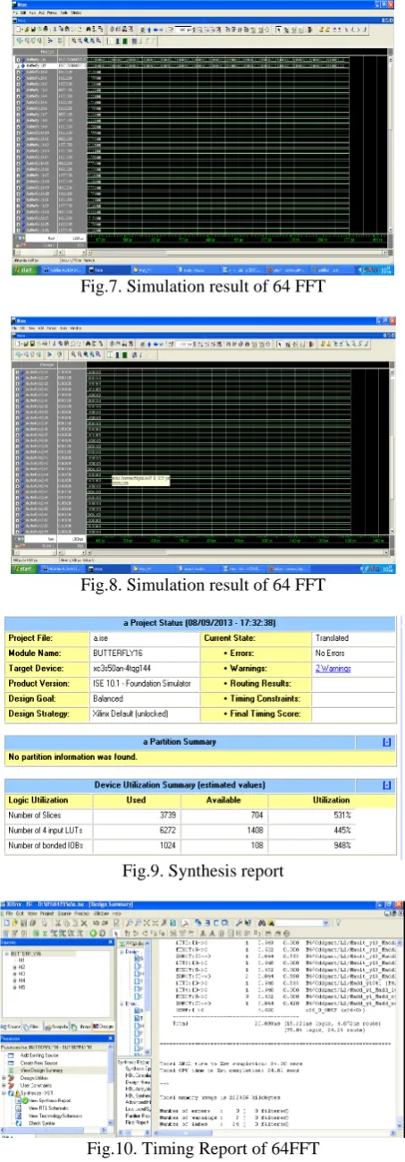
Fig.7. Simulation result of 64 FFT
Fig.8. Simulation result of 64 FFT
Fig.9. Synthesis report
Fig.10. Timing Report of 64FFT
Fig.11.Timing report on Hardware
Fig.12. Result of 64 FFT on Hard ware implementation
V. C
ONCLUSIONThis project it is shown that a baseband ASIC can be fast and at the same time flexible with a low power consumption. The term fast do not refer to extreme clock frequencies but to the fact that no part of the designs needs more than one clock cycle to process a sample once the pipe is filled. Hence, the design does not need to be clocked any faster than the requested bandwidth and compared to modern CMOS technology this is a low number, in the order of 5-100 MHz There are several advantages with a low clock frequency, first is possible use a low power/low speed cell library with low static leakage current and secondly, it is easier to create a clock tree. In addition, there will be more margins to reduce supply voltage if the required clock frequency is low. To have a low leakage power is important in these designs, since flexibility is achieved with independent modules, where the operation mode decides if a module should be used or not. The unused modules are not clocked and hence only consume static leakage power.
R
EFERENCES[1] R. W. Chang, “Synthesis of Band-Limited Orthogonal Signals
for Multichannel Data Transmission,” Bell System Tech. J., vol.
45, pp. 1775–1796, Dec. 1966.
[2] ETS 300401, ETSI, “Digital Audio Broadcasting (DAB);DAB
to mobile, portable and fixed receivers,” 1995.
[3] ETSI EN 300 744, “Digital video broadcasting (DVB);framing structure, channel coding, and modulation for digital terrestrial
television,” 2001.
[4] European IST Project, “Power Aware Communications for Wireless OptiMised personal Area Networks (PACWOMAN),”
http://www.imec.be/pacwoman/.
[5] S. B. Weinstein and P. M. Ebert, “Data transmission by
frequency division multiplexing using the discrete Fourier
transform,” IEEE Transactions on Communications, vol. 19, pp. 628–634, Oct. 1971.
[6] A .Peled and A. Ruiz, “Frequency domain data transmission
using reduced computational complexity algorithms,” in Int.
Conf. Acoustic, Speech, Signal Processing, Denver, CO, 1980, pp. 964–967.
[7] ETSI TS 101 475, “Broadband Radio Access Networks (BRAN); HIPERLAN Type 2 Physical (PHY) layer, v1.1.1,”
2000, http://portal.etsi.org/bran/.
[8] L.J. Cimini, “Analysis and Simulation of a Digital Mobile
Channel Using Orthogonal Frequency Division Multiplexing,”
IEEE Transactions on Communications, vol. 33, pp. 665–675, July 1985.
[9] IEEEstd 802.11a, “High-speed Physical Layer in 5 GHz Band,”
1999, http://ieee802.org/.
[10] IEEE std 802.11g, “High-speed Physical Layer in 2.4 GHz
Band,” 2003, http://ieee802.org/.
[11] J. Bingham, “Multicarrier Modulation for Data Transmission: An Idea Whose Time Has Come,” IEEE Communications
Magazine, vol. 8, pp. 5–14, May 1990
[12] O. Edfors, M. Sandell, J. van de Beek, D. Landström and F.
Sjöberg, “An introduction to orthogonal frequency-division
multiplexing,” TULEA 1996:16, Div. of Signal Processing,
Luleå, Tech. Rep., a University of Technology, Luleå 1996. [13] J. W. Cooley and J. W. Tukey, “An Algorithm for Machine
Calculation of Complex Fourier Series,” Math. Comput., vol. 19,
pp. 297–301, Apr. 1965.
[14] R. Grunheid, E. Bolinth, and H. Rohling, “A blockwise loading
algorithm for the adaptive modulation technique in OFDM
systems,” in Proc. of Vehicular Technology Conference, VTC
2001 Fall, Atlantic City, NJ, USA, Oct. 7-11 2001, pp. 948–951. [15] J. G. Proakis, Digital Communications. McGraw-Hill, 2001. [16] M. Russel and G. Stuber,“Interchannel interference
[17] N. Petersson, “Peak and power reduction in multicarrier
systems,” 2002, licentiate thesis, Lund University, Sweden. [18] S.Johansson, “ASIC Implementation of an OFDM
[19] R. Morrison, L. J. Cimini, and S. K. Wilson, “On the Use of a Cyclic Extension in OFDM,” in Proc. of Vehicular Technology Conference, VTC 2001 Fall, vol. 2, Atlantic City, NJ, USA, Oct. 7-11 2001, pp. 664–668
[20] K. Parhi, VLSI Digital Signal Processing Systems. New York, NY, USA: John Wiley & Sons, 1999.
[21] Hongjiang He and Hui Guo, “The Realization of FFT Algorithm
based on FPGA Co-processor,” Second International
Symposium on Intelligent Information Technology Application, vol. 3, pp.239-243, Dec. 2008.
[22] Transmeta Corporation, “Transmeta Long Run Power Management,”http://www.transmeta.com
[23] ] J. G. Proakis and D. G. Manolakis, Digital Signal Processing. Prentice-Hall, 1996.
[24] S. He, “Concurrent VLSI Architecture for DFT Computing and
Algorithms for Multi-output Logic Decomposition,” Ph.D.
dissertation, Lund University, 1995.
[25] K. Nazifi and G. Hasson, “Industry’s First RTL Power
Optimization Feature Significantly Improves Power Compiler’s Quality of Results,” 1998, www.synopsys.com/news/pubs/rsvp/
spr98/rsvp spr98 6.html.
[26] W. Li and L. Wanhammar, “A Pipelined FFT Processor,” in
IEEE Workshop on Signal Processing Systems, 1999, pp. 654–
662.
[27] S. Johansson, S. He, and P. Nilsson, “Wordlength Optimization of a Pipelined FFT Processor,” in Proc. of 42nd Midwest
Copyright © 2013 IJECCE, All right reserved
A
UTHOR’
SP
ROFILEN. Amarnath Reddy
pursuing M.Tech (VLSI & ES) in GMRIT, Rajam, India. He has completed B.Tech (ECE) from N.I.E, Macherla, India. He is a Student IEEE member from 2012.