Equalization Chargers Using Parallel- or
Series-Parallel-Resonant Inverter for Series-Connected
Supercapacitors
Yifan Zhou and Lei Li
College of Automation, NUST, Nanjing, Jiangsu, 210094, China Email: [email protected], [email protected]
Abstract—A equalization charger using parallel-or series-parallel-resonant inverter for series-connected supercapacitors is proposed in this paper, according to low voltage characteristic of supercapacitor. This topology reduces a large number switches and only has resonant structure including some diodes and a single transformer. In addition, because of the characteristic of parallel resonant inverter, the equalization charging current can be limited in the numerical value. So the topology can work steadily without feedback control. The control circuit is greatly simplified. The simulation results from a 200W universal input prototype are given to verify the effectiveness of the analysis and the merits and demerits of this topology also are introduced.
Index Terms—supercapacitor (SCs), resonant inverter,
equalization charger
I. INTRODUCTION
With the rapid development of the rail transportation today, how to reduce the subway’s energy loss and operating costs is especially important. The research on metro regenerative braking energy recycling is of great significance to the development of rail transportation, the energy conservation as well as the protection of environment. In metro regenerative braking energy recycling systems, supercapacitors (SCs) are widely used to store the regenerative braking energy. However, the voltage equalization of SCs in series is a key technical problem which limits the application of SC storage systems. The equalizers of SCs become research hotspots. A SC voltage equalization charger device used in DC metro traction power grid is studied, and a novel voltage equalization charger circuit is proposed which is promised to achieve a high equalization precision. The equalization device also has other auxiliary functions to guarantee the security and reliability of SCs.
Alongside, a variety of equalization techniques have been proposed to mitigate the voltage unbalance of series-connected Lic and Scs [1]-[4]. But the conventional topology exist too much transformers and switches. So the equalization charger needs a large scale and high weight [5]. The least but not the least, it is rather expensive comparing to this novel topology.
Manuscript received March 5, 2015; revised July 21, 2015.
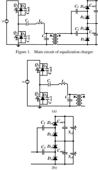
II. OPERATION ANAYSIS OF EQALIZATION CHARGER Fig. 1 is the main circuit of equalization charger. First, the circuit has two parts. Fig. 2 is resonant inverter and voltage multiplier.
Cs Lr
C1
Q1
Q2
Dr1
D1
D2
Co
s
s
1
Co
s
s
2
Co
s
s
1
Dr3
Dr2
Dr4
Cr
C2 Cout1
Cout2
Sc2
Sc1 * *
DC
Figure 1. Main circuit of equalization charger
Cs Lr
Q1
Q2
D1
D2
Cos
s
1
Cos
s
2
Cos
s
1
Cr * *
DC
(a)
C1
Dr1 Dr3
Dr2 Dr4
C2 Cout1
Cout2 Sc2
Sc1
(b)
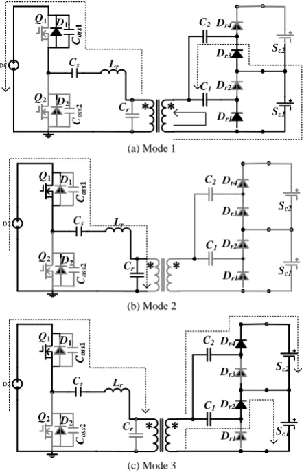
Figure 2. (a) Resonant inverter (b) voltage multiplier
In resonant inverter circuit, a DC source gives the energy to resonance unit. The resonance unit consists of two capacitors Cs Cr and single inductance Lr. Cs plays an
effect as not only resonance unit but also a blocking capacitor. So the Cs need to design much larger than Cp.
Also the equalization current can be designed at high value.
In voltage multiplier circuit, the equalization current from primary side of transformer deliver to transformer secondary side. On account of current flow direction, we can be divided into two types. Firstly, the current inflows into diodes which have the odd-numbered subscript. Secondly, the current inflows into diodes which have even-numbered subscript. These two situations are the same considering the effect on mitigate the Scs. C1 and
C2 have an effect on clamping voltage. Cout is filter
capacitor and it is leaved out when analysis the multiplier.
t 0 0 t t 0 t 0
0 t0 t1 t2t3 t
Q2
VDrv1
v
aiLr
v
criDr1
iDr2
VDrv2
t4 t5
Q1 Q2 Q1
t6 t7
Figure 3. Key operation waveforms under voltage-balanced condition
Cs Lr
C1 Q1 Q2 Dr1 D1 D2 Cos s 1 Cos s 2 Cos s 1 Dr3 Dr2 Dr4 Cr C2 Sc2 Sc1 * * DC
(a) Mode 1
Cs Lr
C1 Q1 Q2 Dr1 D1 D2 Cos s 1 Cos s 2 Cos s 1 Dr3 Dr2 Dr4 Cr C2 Sc2 Sc1 * * DC
(b) Mode 2
Cs Lr
C1 Q1 Q2 Dr1 D1 D2 Cos s 1 Cos s 2 Cos s 1 Dr3 Dr2 Dr4 Cr C2 Sc2 Sc1 * * DC
(c) Mode 3
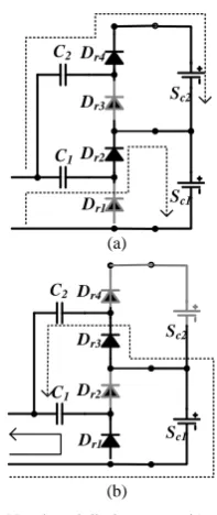
Figure 4. Current flow direction
Waveforms in Fig. 3 are illustrated assuming the components are ideal and Cout is large enough. Fig. 4
illustrates current condition in every state.
Time t0-t1: Current condition are expressed in Fig. 4(a).
The current inflow into fly-wheel diode while Vcp is
clamped to –nVi/2 and iDr1 iDr3 have the current that from
the primary transformer. Lr and Cs happen resonance.
Because before iLr reaches to zero, the driving signal of
Q1 is emerged. So the Q1 can turn on at zero Voltage
(ZVS).
Time t1-t2: When iLr reaches to zero, transformer quit to
the circuit. So Lr Cs Cr resonant. All the diodes in
secondary transformer have no currents. The multiplier does not work. These situations similar with parallel-series resonant. In order to achieve the high equalization charger current, we need to make iLr-max larger. So in this
state, Lr Cs Cr need to design quite small.
Time t2-t3: When Vcr increases to nVi/2, Vcr is clamped
at this value. Cr quit resonance. Voltage multiplier works.
The diodes with even-numbered have the current. So the equalization charger current is sum of every diode current. In other words, the whole equalization charger current can be divided into several Scs.
Time t3-t4: When the driving signal of Q1 is off,
anti-parallel diode D2 can freewheel. So Q2 is ready for ZVS.
The waveforms are similar with the first state. Current situation in t3-t6 is symmetrical to situation in t0-t3.
III. ANALYSISING AND MODELLING FOR VOLTAGE MUTIPLIER
In this section, voltage analysis is showed in this part of article. We can ignoring the Cout because comparing to
Sc, Cout is extremely small.
As showing in Fig. 3 and Fig. 4, the resonant inverter provide to the current only when the Vcp is constant
neither nVi/2 or –nVi/2. The voltage multiplier only
works in these situations so the circuit in Fig. 4(b) is neglected. It is reasonable to analysis Fig. 4(a) and Fig. 4(c).
For clarity, only two supercapacitors discusses in the model. The model also has two states. First the situation while current flow into odd-numbered diodes, on the contrary, the situation while current flow into even-numbered diodes.
According to KVL law, from Fig. 5(a) the secondary voltage of transformer which is input voltage for voltage multiplier can be expressed in following equation.
(r r ) (r r )
S E m Cm E D Cm m D
S E m n Cn E D Cn n D
V V V V I
V V V V V I
(1)
where Vi is the voltage of supercapacitor, VCi-E is voltage
of C1, VD is voltage of diode, Iciis current of diode in
conduction angle. riand rDare resistance of SC and diode.
Also According to KVL law, from Fig. 5(b) the secondary voltage of transformer which is input voltage for voltage multiplier can be expressed in following equation.
(r r ) (r r )
S O Cm O D Cm m D
S O m Cn O D Cn n D
V V V I
V V V V I
C1
Dr1 Dr3
Dr2 Dr4 C2
Sc2
Sc1
(a)
C1
Dr1
Dr3
Dr2
Dr4
C2
Sc2
Sc1
(b)
Figure 5. (a) Even-Numbered diodes are on (b) odd-numbered diodes are on
In practical, the outer capacitor flows larger current when the input voltage is larger. So it is necessary to use outer capacitors to reduce current of SC.
Because two states are symmetrical, the input voltages of voltage multiplier are the same.
S E S O S
V V V (3) According to (1), (2):
2
2 2 ( )
C i Ci O Ci E
S i D Ci i D
V V V
V V V I r r
(4)
In general, the variation of capacitor can be expressed in following equation.
eq
It I
V IR
C Cf
(5)
2 2
2
Ci
S i D eq i
I
V V V R (6) where Req-i is equivalent resistance of voltage multiplier
1 2
2{ ( )}
eq i i D
i
R r r
C f
(7)
1 ( / 2)1
c
V V (8)
2 ( 2/ 2+ )1
c
V V V (9) So the voltage multiplier can be modeled as the following equivalent circuit.
The input voltage of multiplier doubles as 2Vs, while
the current halved as IVM/2. IVM/2 equals to sum of every
Sc equalization charger current. IVM/2 automatically
distributes more current into the Sc which has lower voltage than the other SCs. In conclusion, the voltage multiplier can equal SCs’ voltage automatically, without
having voltage detection module. The voltage precision of equalization charger depends on Req-I (7). Req-i includes
the equivalent resistance of Ci, Sc and diode. If the values
of three factors C1 r1 and rD are all the same as the value
of another three factors, the voltage of the Sc1 and Sc2 will
be identical. In other words, the effect of the equalization is excellent.
IV. DESGIN GUIDE
In this section, a design guide will be discussed. A equalization charger using parallel resonant inverter is designed to charge 8 supercapacitors. These 8 supercapacitors have different initial voltages. These voltages are 1.1V, 1.2V, 1.3V, 1.4V, 1.5V, 1.6V, 1.7V, 1.8V. The maximum power is 200W when the input voltage dc source is 100V. Q1 and Q2 work at the frequency of 195kHz. A voltage multiplier consist of Ci
(Ci=100uF, ri=100mΩ) and diodes (VD=0.38, rD=20mΩ).
2VS
IVM/2
D1 D2
D3 D4
Req1 Req2
B1 B2
Ic1/2
Ic2/2
Figure 6. Equivalent of voltage multiplier
According to Fig. 6, IVM is the sum of Ici/2 which is the
equalization charger current toward supercapacitor. Under a voltage-balanced condition:
1 ... 8 200[W] 2[A]
2 2 2 100[V]
VM c c
I I I
(10) 1
2 o
r r
f
L C
(11)
Then Lr is designed to be 25uH while Cr is 30n, Cs is
designed to be 1u and it is much larger than Cr.
V. SIMULATION RESULT
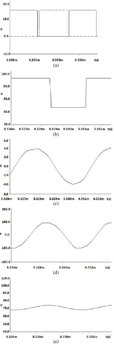
Simulate in Saber. The parameters of the prototype are as follows:
1) Input voltage: vin100V;
2) Equalization charger current: Ieq2A;
3) Equalization charger power: Peq200W; 4) Switching frequency of the converter: 195kHz The parameters of the PRI stage are as follows:
1) Magnetizing inductance: Lr22uH;
2) Resonance capacitor: Cr30nF
3) Blocking capacitor: Cs1uF
4) Duty ratio: n4; 5) Supercapacitor: Sc200F
Fig. 7 shows the waveforms of constant duty cycle, the input voltage of resonance unit, current of Lr, the voltage
of Cp, the voltage of Cs, the current of iVM and
even-numbered and odd-even-numbered Diode under voltage-balanced condition.
Finally Substitution (5) into (4):
In Fig. 7(a), Duty cycle is 49.7% in order to prevent short circuit of Q1 and Q2.
In Fig. 7(d), it can be seen that when the voltage of Cp
is clamped to-nVi/2 and +nVi/2, the voltage multiplier
works. Energy from PRI distributes to the SCs to achieve
the purpose of equalization charging.
In Fig. 7(e), it can be seen that Cs plays a role of not
only the resonance unit component but also blocking capacitor.
In Fig. 7(f), iVM in the duty is different from the next
duty because the Scs is charging that means the changes
on the voltages of Scs influence iVM.
(a)
(b)
(c)
(d)
(e)
(f)
(g)
Figure 7. Simulation waveforms (a) constant duty cycle (b) the input voltage of resonance unit (c) current of Lr, (d) the voltage of Cp (e) the
voltage of Cs (f) the current of iVM (g) current of even-numbered (dotted
line) and odd-numbered Diode (solid line)
(a)
(b)
Figure 8. Equlization of Sci (a) the voltage of Sc1 and Sc8 (b) the current of even-numbered and odd-numbered Diode
Fig. 8(a) shows the waveform of voltage of Sc1 and Sc8 and the current of even-numbered and odd-numbered Diode.
Because of large capacitor of Sc, the simulation time is extremely long. So in this situation use 10mF value instead of 200F.
It can be seen from this waveform that the voltage of Sc1 and Sc8 from unbalanced situation to balanced situation. The result is excellent using this topology.
VI. CONCLUSIONS
The equalization charger using parallel resonance and voltage multiplier has the advantage of topology simple and efficient, widely used in small and medium power applications while the volume of passive components constraint its further improve of the power density. A 200-W prototype of the proposed equalizer for 8 supercapacitors connected in series was built. The voltage of SCs initially different and imbalance eventually eliminates, then become the same voltage level.
ACKNOWLEDGMENT
Project 51177073 supported by National Natural Science Foundation of China.
REFERENCES
[1] C. S. Moo, Y. C. Hsieh, and I. S. Tsai, “Charge equalization for series-connected batteries,” IEEE Trans. on Aerospace and Electronic Systems, vol. 39, no. 2, pp. 704-710, Apr. 2003. [2] M. J. Isaacson, R. P. Hollandsworth, et al., “Advanced lithium ion
battery charger,” in Proc. Battery Conference on Applications and Advances, 2000, pp. 193-198.
[3] Y. S. Lee, M. W. Cheng, S. C. Yang, and C. L. Hsu, “Individual cell equalization for series connected lithium-ion batteries,” IEICE Transactions on Communications, vol. 89, no. 9, pp. 2596-2607, Sep. 2006.
[4] Y. S. Lee and M. W. Cheng, “Intelligent control battery equalization for series connected lithium-ion battery strings,”
IEEE Trans. on Industrial Electronics, vol. 52, no. 5, pp. 1297-1307, Oct. 2005.
[5] M. Uno and K. Tanaka, “Double-Switch single-transformer cell voltage equalizer using a half-bridge inverter and voltage multiplier for series connected supercapacitors,” IEEE Trans. Veh. Technol., vol. 61, no. 9, pp. 3920-3930, Nov. 2012.
Yifan Zhou was born in Nanjing, China, in
1991, received the B.S. degree from the Electrical engineering and automation, Nanjing Normal University, Nanjing, China in 2013. He is currently working towards the M.S. degree in power electronics and power transmission at collage of Automation, Nanjing University of Science and Technology, Nanjing, China. His research interests include supercapacitor equalizer technique.
Lei Li (M’09) received the B.S. degree from
the Department of Electrical Engineering, Shandong University of Science and Technology, Qingdao, China, in 1997, and the Ph.D. degree from the Department of Electrical Engineering, Nanjing University of Aeronautics and Astronautics, Nanjing, China, in 2004.