Memory Efficient LUT Based Address Generator
for OFDM-WiMAX De-Interleaver
Bijoy Kumar Upadhyaya
1, Pranab Kumar Goswami
1, and Salil Kumar Sanyal
2 1Department of Electronics & Telecommunication, Tripura Institute of Technology, Narsingarh, Tripura, India 2Department of Electronics & Telecommunication, Jadavpur University, Kolkata, India
Email: [email protected], [email protected], [email protected]
Abstract—In this paper, a memory efficient Look-up Table (LUT) based address generator for the de-interleaver used
in OFDM-WiMAXtransreceiver is proposed. The
relationships between various address LUTs implementing different interleaver / de-interleaver depths within a modulation scheme have been exploited to model the proposed address generator. The proposed design shows 81.25% saving of memory blocks in comparison with conventional technique. Hardware structure of the address generator is developed and is converted into a VHDL model using Xilinx Integrated Software Environment (ISE). Simulation results obtained using ModelSim XE-III verifies the functionality of the proposed design. Comparative study of FPGA implementation results of the design on two different platforms is presented. Performance improvement of approximately 30% in terms of maximum operating frequency over a recent work is also obtained.
Index Terms—address generator, de-interleaver, FPGA, LUT, OFDM, VHDL, WiMAX
I. INTRODUCTION
Broadband Wireless Access (BWA) has become a popular choice over Digital Subscriber Line (DSL) or
cable modem for internet access. Worldwide
Interoperability for Microwave Access (WiMAX) is based on IEEE 802.16 standard for BWA system. The fixed BWA (FBWA) is based on IEEE 802.16-2004 and operates in the frequency band of 2 to 11GHz [1]. Amendment IEEE 802.16e adds mobility support to IEEE 802.16 and defines standard for mobile BWA (MBWA) in the frequency band 2 to 6GHz. Typical data rate in IEEE 802.16e is 5Mbps with bandwidth 1.25 to 20 MHz. Both IEEE 802.16-2004 and IEEE 802.16e permit Non Line of Sight (NLOS) connectivity [2].
Orthogonal Frequency Division Multiplexing (OFDM) [2] technique offers promising solution that has gained tremendous research interest in recent years due to its high transmission capability and alleviating the adverse effects of Inter Symbol Interference (ISI) and Inter Channel Interference (ICI) ability. In an OFDM system, the data is divided into multiple parallel sub-streams at a reduced data rate, and each is modulated and transmitted on a separate orthogonal subcarrier. This increases
Manuscript received October 14, 2013, revised January 23, 2013. This research is supported by The Institution of Engineer (India), Kolkata, India. Project id is UG2013007.
symbol duration and improves system robustness. OFDM is achieved by providing multiplexing on users’ data streams on both uplink and downlink transmissions. OFDM is the fundamental building block of the IEEE 802.16 standard.
Interleaving plays an important role in improving the performance of Forward Error Correcting (FEC) codes in terms of bit error rate. Interleaving is a process to rearrange code symbols so as to spread burst of errors into random like errors and thereafter FEC techniques can be applied to correct them. Block interleaving is one of the widely used techniques for interleaving in which the bits received from the encoder are stored row wise in the interleaver’s memory and read column wise. WiMAX uses a special type of block interleaver in which the channelinterleaver depth and pattern varies based on code rate and modulation type.
In this paper, we propose a novel technique to implement the address generator used in OFDM-WiMAX de-interleaver. The conventional Look-Up Table (LUT) based technique for address generation has been re-designed to use the memory blocks efficiently. During this work, it has been observed that within a modulation scheme the address LUT of a smaller interleaver depth is the subset of the address LUT of larger interleaver depth in WiMAX de-interleaver address generator. This relationship between the address LUTs is used to propose a novel memory efficient LUT based address generator for WiMAX de-interleaver. The proposed scheme shows 81.25 % improvement in terms of saving memory blocks. A hardware structure for the proposed LUT based de-interleaver address generator is designed and is transformed into a VHDL model using Xilinx Integrated Software Environment (ISE). The model is then implemented on two reconfigurable platforms and comparative analysis in term of FPGA resources / parameters between the two is also presented. Based on the equivalence drawn using [3], our implementation shows betterment of approximately 30% over [4] in terms of maximum operating frequency.
II. SYSTEM DESCRIPTION
which will cause timing recovery problem at the receiver. Pseudo Random Binary Sequence (PRBS) is used in which randomization is done by modulo 2 addition of the data with the output of the PBRS itself [5]. The randomized data bits are thereafter encoded using Reed Solomon (RS) encoder followed by Convolutional Coder (CC). The former is suitable for correction of burst type of error whereas the later is for random error. After RS-CC encoding all encoded data bits shall be interleaved by a special type of block interleaver. Thereafter, data passes through the mapper block in which modulation takes place. The resulting data symbols are used to construct one OFDM symbol by performing Inverse Fast Fourier Transform (IFFT).
In the receiver, inverse blocks are applied which perform DFT, de-mapping, de-interleaving, decoding and de-randomizing operations in sequential manner to get back the original data sequence.
III. INTERLEAVING / DE-INTERLEAVING IN WIMAX
The WiMAX block interleaver/de-interleaver exploits different Interleaver depths (Ncbps) to incorporate various code rates and modulation schemes and isdescribed in standard documentfor IEEE 802.16e [6]. The Encoded data bits received from CC are interleaved by a block interleaver using two step processes [7]. The first step ensures that the adjacent coded bits are mapped onto nonadjacent subcarriers, which provides frequency diversity and improves the performance of the decoder. The second step ensures that adjacent coded bits are alternately mapped to less and more significant bits of the modulation constellation thus avoiding long runs of lowly reliable bits.
The de-interleaver, which performs the inverse operation, is also defined by another two permutations and is described in [4].
Figure 1. Block diagram of WiMAXtransreceiver
IV. MODELING MEMORY IN FPGA
Static Random Access Memory (SRAM) based FPGAs [8] offer internal (embedded) storage for potential applications like local storage, FIFO, data buffers, stack, large LUT etc. In Xilinx FPGA, these internal storages are called Block RAM (BRAM) [9]. Table I and Fig. 2 list all the interface signals of a single port BRAM and their directions. In our experimentation, Xilinx Spartan-3/Spartan-3AN FPGA (device XC3S1400AN) [8] having 16/32 nos. of 18KB (16KB data and 2KB parity) single port BRAM block is used. Out of these, 3 BRAM blocks
are used to store the address LUTs for three different modulation schemes of WiMAX de-interleaver address generator.
V. HARDWARE MODEL OF INTERLEAVER
A. Methodology of Proposed Design
In general, design methodology of hardware
interleaver is classified into two categories, LUT based and incremental address generation based. The former technique is relatively simple but consumes large logic resources, particularly memory, whereas the later involves complex design methodology but requires relatively less logic resources. In this work, the authors propose an improved design methodology to implement the LUT based address generator for WiMAX de-interleaver on reconfigurable platform. As per IEEE 802.16e standard [6], ½, ⅔ and ¾ are the allowed code rates where as QPSK, 16-QAM and 64-QAM are the permitted modulation schemes. Accordingly, there are eight, four and four interleaver depths in QPSK, 16-QAM and 64-QAM modulation schemes respectively [7] to implement all the permissible code rates and modulation schemes. In conventional LUT based approach, to implement the de-interleaver address generator, 16 numbers of memory blocks of varying size are required to house all the interleaver addresses. During this work, a relationship between the de-interleaver memory addresses of various Ncbps within a modulation scheme is identified. It is found that, the memory addresses of a larger Ncbpsencompass the same of smaller Ncbps. This relationship between the address LUTs is exploited to propose a memory efficient LUT based address generator for WiMAX de-interleaver. Using our proposed design, the number of memory blocks used is reduced to 3 only ensuring saving of 81.25% critical resource.
Figure 2. Single port BRAM in Xilinx Spartan-3AN FPGA
TABLE I. SINGLE PORT BRAM INTERFACE SIGNAL
Signal Description Port Name Direction
Data Input Bus DI Input
Parity Data Input Bus DIP Input Data Output Bus DO Output Parity Data Output DOP Output
Address Bus ADDR Input
Write Enable WE Input
Clock Enable EN Input
Synchronous Set/Rest SSR Input
Clock CLK Input
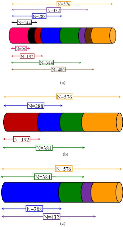
de-interleaverfor all code rates and modulation schemes. Among these addresses, first 5 rows for each modulation schemes with Ncbps = 576-bits are presented in Table II(a)-(c). The first 6 columns in Table II(a), describe the memory addresses of first 5 rows with Ncbps = 96-bits and QPSK modulation scheme. Similarly, the first 5 rows of interleaver memory addresses with Ncbps = 144-bits and QPSK modulation scheme are represented by the first 9 columns in Table II(a). Likewise, the addresses for other Ncbps with QPSK modulation scheme can be determined from the same table where the number of columns is defined as Ncbps/d (here d = 16). A similar approach can be applied in Table II(b) and (c) to determine the memory addresses with various interleaver depths for 16-QAM and 64-QAM modulation schemes respectively. Pictorial representation of this relationship of memory addresses between various interleaver depths are given in Fig. 3(a)-(c).
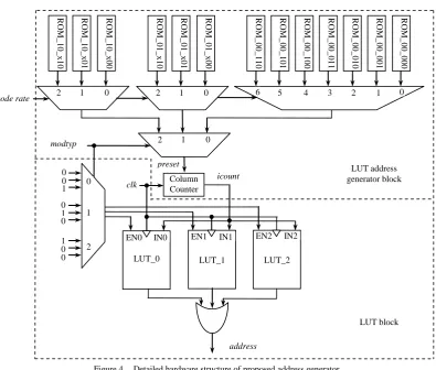
B. Proposed Hardware for the Address Generator The hardware structure of the proposed LUT based address generator for WiMAX de-interleaver is shown in Fig. 4. The complete hardware is divided into two parts: LUT address generator block and LUT block. The former consists of ROMs, multiplexers and an up counter responsible for generating the memory address (icount) required to read the address LUTs. The ROMs store the terminal values of each row as input and the starting values of the next row as the output. The column counter counts up to the desired column and then gets reloaded with another preset value representing the starting memory address of the next row from the appropriate ROM selected by mod typ and code rate signals. The contents of a ROM used to implement Ncbps = 96 of QPSK (ROM_00_000) is presented in Table III. Similar content are available in other ROMs.
The later block contains the three address LUTs storing the de-interleaver addresses for the three modulation schemes. The multiplexer arrangement along with values in the mod typ ensures selection of proper
address LUT for a particular modulation scheme. The selected address LUT is read using icount and the de-interleaver addresses are made available at the address output line.
(a)
(b)
(c)
Figure 3. Relationship between de-interleaver memory address with various Ncbps (= N) and a) QPSK modulation scheme.b) 16-QAM
modulation scheme. c) 64-QAM modulation scheme
TABLE II(A). FIRST FIVE ROWS OF ADDRESSES FOR NCBPS = 576, ¾ CODE RATE, QPSK
0 16 32 48 64 80 9 6 112 128 144 160 176 192 208 224 240 256 272 288 304 320 336 352 368 384 400 416 432 448 464 480 496 512 528 544 560
1 17 33 49 65 81 9 7 113 129 145 161 177 193 209 225 241 257 273 289 305 321 337 353 369 385 401 417 433 449 465 481 497 513 529 545 561
2 18 34 50 66 82 9 8 114 130 146 162 178 194 210 226 242 258 274 290 306 322 338 354 370 386 402 418 434 450 466 482 498 514 530 546 562
3 19 35 51 67 83 9 9 115 131 147 163 179 195 211 227 243 259 275 291 307 323 339 355 371 387 403 419 435 451 467 483 499 515 531 547 563
4 20 36 52 68 84 100 116 132 148 164 180 196 212 228 244 260 276 292 308 324 340 356 372 388 404 420 436 452 468 484 500 516 532 548 564
TABLE II(B). FIRST FIVE ROWS OF ADDRESSES FOR NCBPS = 576, ¾ CODE RATE, 16-QAM
0 16 32 48 64 80 9 6 112 128 144 160 176 192 208 224 240 256 272 288 304 320 336 352 368 384 400 416 432 448 464 480 496 512 528 544 560
17 1 49 33 81 65 1 1 3 9 7 1 4 5 1 2 9 1 7 7 1 6 1 2 0 9 1 9 3 2 4 1 2 2 5 2 7 3 2 5 7 3 0 5 2 8 9 3 3 7 3 2 1 3 6 9 3 5 3 4 0 1 3 8 5 4 3 3 4 1 7 4 6 5 4 4 9 4 9 7 4 8 1 5 2 9 5 1 3 5 6 1 5 4 5
2 18 34 50 66 82 9 8 114 130 146 162 178 194 210 226 242 258 274 290 306 322 338 354 370 386 402 418 434 450 466 482 498 514 530 546 562
1 9 3 51 35 83 67 115 9 9 147 131 179 163 211 195 243 227 259 275 307 291 339 323 371 355 387 403 435 419 467 451 499 483 515 531 563 547
4 20 36 52 68 84 100 116 132 148 164 180 196 212 228 244 260 276 292 308 324 340 356 372 388 404 420 436 452 468 484 500 516 532 548 564
TABLE II(C). FIRST FIVE ROWS OF ADDRESSES FOR NCBPS = 576, ½ CODE RATE, 64-QAM
0 16 32 48 64 80 9 6 112 128 144 160 176 192 208 224 240 256 272 288 304 320 336 352 368 384 400 416 432 448 464 480 496 512 528 544 560
17 33 1 65 81 49 113 129 9 7 161 177 145 209 225 193 257 273 241 305 321 289 353 369 337 401 417 385 449 465 433 497 513 481 545 561 529
34 2 18 82 50 66 130 9 8 114 178 146 162 226 194 210 274 242 258 322 290 306 370 338 354 418 386 402 466 434 450 514 482 498 562 530 546
3 19 35 51 67 83 9 9 115 131 147 163 179 195 211 227 243 259 275 291 307 323 339 355 371 387 403 419 435 451 467 483 499 515 531 547 563
Figure 4. Detailed hardware structure of proposed address generator
VI. SIMULATION Results
The simulation result in the form of timing diagram obtained using ModelSim Xilinx Edition-III for QPSK (mod_typ = 00) with Ncbps = 144 (code_rate = 001), is shown in Fig. 5. The captured portion shows the de-interleaver addresses generated for the first three rows and are identical with Table II(a). The authors have generated and verified addresses for all coding rates and modulation schemes however due to space limitation other results are not included.
VII. FPGA IMPLEMENTATION Results
The proposed hardware structure of de-interleaver address generator is transformed into VHDL model using Xilinx Integrated Software Environment (ISE 8.1) and is implemented on Xilinx Spartan 3 FPGA (XC3S400). Additionally, the hardware structure is also implemented on Xilinx Spartan-3AN FPGA (XC3S1400AN) using ISE 12.1. Table IV shows the device utilization summary for
both implementations. The two implementations are almost identical in terms of FPGA resource utilizations, but differ significantly in operating frequency and estimated power consumption. It is observed that the design implemented on advanced FPGA (Spartan-3AN) works faster by 30% than the other, but also consumes double amount of power. The principal advantage of our proposed technique is that it requires only 3 BRAMs of capacity 18KB instead of 16, saving 81.25% of critical FPGA internal resource.
Based on the equivalence drawn between FPGA and ASIC implementations in [3] our work is compared with that of [4] by converting the later in FPGA equivalent
implementation. This comparison shows our
implementation on Spartan 3 FPGA is at par with [4] in terms of operating frequency. But, the implementation on Spartan 3AN shows improvement of almost 30% over [4] as FPGA equivalent maximum frequency of the later is found to be 62.5MHz.
Figure 5. Simulation result showing initial addresses of Ncbps = 144 bits of QPSK modulation scheme
R O M _ 0 0 _ 0 1 1 0 1 3 4 5
6 2
Column Counter preset icount clk code rate R O M _ 0 0 _ 1 0 0 R O M _ 0 0 _ 1 0 1 R O M _ 0 0 _ 1 1 0 R O M _ 0 0 _ 0 1 0 R O M _ 0 0 _ 0 0 1 R O M _ 0 0 _ 0 0 0 0 1 2 R O M _ 0 1 _ x 1 0 R O M _ 0 1 _ x 0 1 R O M _ 0 1 _ x 0 0 0 1 2 R O M _ 1 0 _ x 1 0 R O M _ 1 0 _ x 0 1 R O M _ 1 0 _ x 0 0 0 1 2
LUT_0 LUT_1 LUT_2
EN0 IN0 EN1 IN1 EN2 IN2
TABLE III. ROM_00_000
Input Output Input Output
5 36 293 324
41 72 329 360
77 108 365 396
113 144 401 432
149 180 437 468
185 216 473 504
221 252 509 540
257 288 545 0
TABLE IV. DEVICE UTILIZATION SUMMARY
FPGA Resources / Parameters
Resource Utilization / Parameters in
Spartan 3
Resource Utilization / Parameters in Spartan 3AN Number of slices 633 out of 3584 626 out of 11264 Number of slice flip
flops
56 out of 7168 41 out of 22528 Number of 4 input
LUTs
1229 out of 7168 1205 out of 22528 Number of bonded
IOBs
16 out of 141 16 out of 502 Number of BRAMs 3 out of 16 3 out of 32 Number of GCLKs 1 out of 8 1 out of 24 Maximum clock speed 62.5 MHz 88.72 MHz
Power consumption 32mW 68mW
VIII. CONCLUSION
In this paper, a novel technique to model the LUT based de-interleaver address generator for WiMAX system is proposed. A special relationship between the address LUTs has been explored and utilized to propose memory efficient design. The design is transformed into a digital hardware and is implemented on two different reconfigurable platforms. Comparative analysis with one of the existing implementation has been made to highlight improvement in the present work.
REFERENCE
[1] A. Ghosh, D. R. Wolter, J. G. Andrews, and R. Chen, “Broadband wireless access with WiMAX/802.16: Current performance benchmarks and future potential,” IEEE Commun. Mag., vol. 43, pp. 129–36, Feb. 2005.
[2] U. S. Jha and R. Prasad, OFDM towards Fixed and Mobile
Broadband Wireless Access, Artech House Publisher, London,
2007.
[3] I. Kuon and J. Rose, “Measuring the gap between FPGAs and ASICs,” in Proc. Int. Symposium on Field Programmable Gate
Arrays, Monterey, California, USA, ACM Press, New York, 2006,
pp. 21–30.
[4] R. Asghar and D. Liu, “2D realization of WiMAX channel interleaver for efficient hardware implementation,” in Proc. World
Academy of Sc. Engineering and Technology, vol. 51, Hong Kong,
2009, pp. 25-29.
[5] “Local and metropolitan networks—part 16: Air interface for fixed broadband wireless access systems,” IEEE 802.16-2004, 2004.
[6] “IEEE standard for local and metropolitan area networks—part
16: Air interface for fixed broadband wireless access systems—
amendment 2,”IEEE 802.16e-2005, 2005.
[7] B. K. Upadhyaya, I. S. Misra, and S. K. Sanyal, “Novel design of address generator for WiMAX multimode interleaver using FPGA based finite state machine,” in Proc. 13th Int. Conf. Computer and
Information Technology, Dhaka, 2010, pp. 153-158.
[8] Xilinx Spartan-3AN FPGA Family Datasheet. [Online]. Available:
http://www.xilinx.com
[9] Xilinx. Using block RAM in Spartan 3 FPGAs. XAPP463. [Online]. Available: www.xilinx.com
Bijoy Kumar Upadhyaya received the B. Tech degree in Electronics and Communication Engineering from North Eastern Regional Institute of Science and Technology (NERIST), Itanagar, India in 1998 and the Master of Electronics and Tele-communication Engineering from Jadavpur University, Kolkata, India in 2007. He joined Tripura Institute of Technology, TIT (erstwhile known as Polytechnic Institute), Narsingarh, Tripura, India as Lecturer in 2000. He is presently working as Associate Professor and Head in Electronics and Tele-communication Engineering Department of TIT, Narsingarh. He is member of IEEE, Life member of Institution of Engineers (India) and Institution of Electronics and Telecommunication Engineering. He has several publications in peer reviewed journals and international and national conferences. His research area is error control coding and its application in digital communication and digital system design using hardware description languages.
Pranab Kumar Goswami received B.E. Electronics and Telecommunication Engineering from Tripura Institute of Technology, Narsingarh, Tripura in 2012. He is presently working as Teaching Assistant in the same Institute. His area of interest includes communication engineering and electromagnetic theory.