Please cite this article as: L. Maharana, T. Sarkar, S. Nath Pradhan, Look up Table Based Low Power Analog Circuit Testing, International Journal of Engineering (IJE), TRANSACTIONSC: Aspects Vol. 29, No. 9, (September 2016) 1247-1256
International Journal of Engineering
J o u r n a l H o m e p a g e : w w w . i j e . i r
Look up Table Based Low Power Analog Circuit Testing
L. Maharana, T. Sarkar*, S. Nath Pradhan
Department of Electronics and CommunicationEngineering, National Institute of Technology Agartala, Tripura, India
P A P E R I N F O
Paper history: Received 11 May 2016
Received in revised form 11 July 2016 Accepted 14 July 2016
Keywords:
Oscillation-based Built in Self-test (OBIST) Look up Table (LUT)
Analog Testing Operational Amplifier Fault Coverage Low Power Current Correlator
A B S T R A C T
In this paper, a method of low power analog testing is proposed. In spite of having Oscillation Based Built in Self-Test methodology (OBIST), a look up table based (LUT) low power testing approach has been proposed to find out the faulty circuit and also to sort out the particular fault location in the circuit. In this paper an operational amplifier, which is the basic building block in the analog circuit, is designed and is taken for testing purpose. Fault coverage is identified after fault modeling, fault injection and fault simulation. More than 93% fault coverage is achieved and there is a scope of increasing more fault coverage. Since analog testing prefaces the challenge of power dissipation during testing, some power minimization techniques like sleepy stack method and current correlation method have adhered during the testing process. Test power reduction up to 84 % is achieved in this work.
doi: 10.5829/idosi.ije.2016.29.09c.10
1. INTRODUCTION1
The revolution and evolution in System-on-Chips (SoCs) design increases the complexity of circuit due to increase in transistor count according to the Moore’s law. In a nano space wafer, it is harder to integrate a circuit having millions of transistors with perfection. Due to continuous dimensional modulation the circuit geometry shrinks which increases the sensitivity of circuit performance. Testing is highly essential to sort out a fault-free circuit after the batch process of IC (integrated circuits) design and before packaging. There may be a chance of transistor missing or redundant device addition at the time of circuit fabrication. Since ICs are manufactured in a batch process, the same type of error is found and can be rectified at the structural level. Base level testing would save time, improve quantification of cost and yield along with customer satisfaction. Therefore, prototypic testing for circuits is essential before going to the production cycle.
In the testing process behavior and response of the testing circuit is checked according to the given input. It
1*Corresponding Author’s Email: [email protected] (T.
Sarkar)
is the process of realization to ensure whether the circuit is free from defects or not. Different circuit imperfections may lead to failure of individual ICs.
ICs consist of both analog and digital blocks interfaced by an ADC or a DAC. Since the required supply voltage and the output voltage of analog and digital blocks are different, testing should be held separately. In the case of digital testing the output has two probable values like VDD (logic ‘1’) or GND (logic ‘0’) irrespective of the type of faults or inputs. Therefore, test pattern generation is quite simple. But for the analog module, a range of outputs can be possible due to high sensitivity and varying tolerance of analog parameters. So test pattern generation is difficult for analog testing. In some testing approaches like Oscillation-based Built-in Self-Test (OBIST) [1] there is no such pattern generator or pattern analyzer which is present in digital testing. In addition, fault simulation is often used to access the effectiveness of a set of test vectors in detecting faults that might occur during manufacturing. In contrast, the analog circuit design is less structured and lacking proper design for testability method. Therefore, in this paper we are going for analog
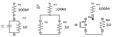
Figure 1. Stuck-open and Stuck-short fault models for capacitor, resistor, and MOSFET
testing that confront a general solution. Here identification of both faulty circuit and the faulty node in the circuit has been discussed with some advantages as compared to OBIST technique. Since analog signal testing is a partition based testing, each module is tested separately.
Operational amplifier (Op-Amp) is the basic building block for many analog circuits, and the theoretical behavioral values of operational amplifier match with its practical behavior; it has been taken as the base circuit for analog testing in this paper. Reduction of power dissipation is also an important task during the testing process as testing circuit consumes more power as compared to a normal circuit and in low power VLSI design power dissipation plays a major controller for a better and relevant design. Therefore, power reduction during testing is a necessary step for a successful testing and power is successfully reduced for many digital circuits during testing. But less attention has been paid on the issue of power reduction during analog testing. Hence in this paper some techniques like sleepy stack and current correlators are being proposed for power reduction during analog testing.
The rest of the paper is organized as follows. Section 2 deals with the literature review of analog circuit testing. Proposed work is detailed in section 3. Section 4 describes the power minimization technique during testing. Section 5 enumerates the experimental results. The paper is concluded in section 6.
2. LITERATURE REVIEW
A novel BIST (Built in Self-Test) has been described in [1]. In this paper the test approach is based on oscillation strategy. An ADC (Analog to Digital Converter) has been taken as CUT (Circuit under Test) for functional testing. In [2] it has been described about different types of faults, those are frequently observed during testing such as stuck open, stuck short and how to model those faults for testing. Stuck open means open circuit between any two connected terminals and is modeled by connecting a resistor having resistance nearly equal to 100MΩ (very high value) as shown in Figure 1. Similarly stuck short means short circuit of any two connectionless terminals and is modeled by connecting the two terminals with a resistor of nearly
10Ω resistance (very low value). In Figure 1 third diagram is the fault model for a MOSFET having both the faults. The open terminal at the source is modeled by connecting it with 100MΩ resistor for modeling of stuck short fault. To model stuck short fault, the source and drain terminals are connected by a 10Ω resistor.
In [3], Built in Self Test method is adopted to check the functionality of analog circuit. Unlike the OBIST method here a time-division multiplexing (TDM) comparator is used to analyze the response of a circuit under test with minimum hardware overhead. TDM comparator can be used to measure the frequency and amplitude. In this technique also the CUT is converted into an oscillator.
In [4], an extra Schmitt trigger is used as the on chip frequency reference to compensate the influence of process parameter variations. However this solution can be also implanted in OBIST method for analog circuits. The proposed OBIST strategy has been experimentally applied to verify various circuits like filters. It is applicable to determine catastrophic faults of the circuit. In [5] systematic steps are followed to find the faulty circuit by Oscillation-Based Built-In Self-Test (OBIST) method and how to calculate fault coverage for a particular testing parameter. Though OBIST method is a successful method of testing at the beginner level but still there are some drawbacks like:
i. It is a manual process i.e. at a time only one fault is being inserted and the response is compared at the output.
ii. It is a complex task to convert every analog circuit into an oscillator circuit before testing procedure. This oscillator circuit becomes a complex circuit which draws large amount of power from the supply.
iv. No power reduction techniques have been developed during analog testing.
v. It would be an efficient testing technique if we would find out the particular faulty node from the circuit which is responsible for the failure of the circuit.
vi. The limited number of parameter test could not be sufficient to conclude a circuit to be faulty.
3. PROPOSED WORK
In the literature, it has been discussed to check whether the analog module is faulty or fault-free. From the marketing point of view, separating the faulty module from that of fault free module results in improved qualitative as well as quantitative product marketing. On the other side as per the manufacturing point of view, it is necessary to find out the faulty circuit and the fault node of that faulty circuit.
Injecting faults one by one and checking the outputs accordingly is a time consuming process. It would be better to test the faults as per the priority of occurrence. Most frequently observed faults should be tested first as compared to the faults having low priority. All the above issues have been addressed in the proposed approach of analog testing. An operational Amplifier of inverting type is taken as the Circuit under Test (CUT) for analog testing. After fault modeling each fault is injected and simulated sequentially as explained in subsequent section.
As we know, the testing circuit consumes nearly double power than the standard circuit. So if power dissipation increases in the circuit the temperature of the circuit will also increase. As a result, the components in the circuit may burn out which may lead to detect a circuit faulty though it is fault free. Therefore, power dissipation should be minimized during testing.
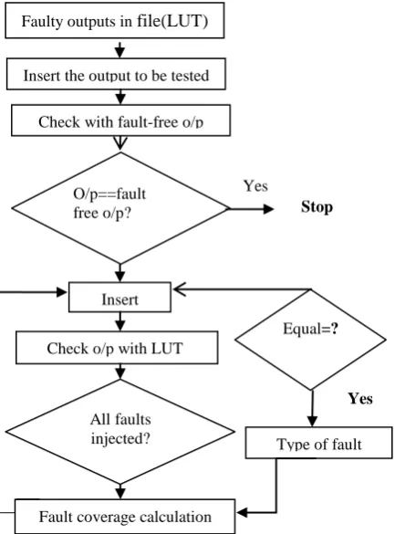
Figure 2. Flowchart of proposed testing hierarchy
In this work, a programming approach has been adopted to find out the faulty circuit and also the fault part of the circuit.The flowchart of the proposed method is given in Figure 2.
A LUT is prepared for the output voltages of the fault models and fault free model of op-amp after the simulation in cadence tool for same time using 45nm technology. The results of the faulty circuit are then compared with the fault-free circuit. While comparing the outputs, a range of output is considered for fault free one. After comparison if the result matches then we can say that it is the fault-free circuit. But to find out the faulty node all the fault outputs are stored in files as reference. That is the Look up Table for the testing. Then while finding the fault type the output of the circuit to be tested is compared with the faulty reference data. The node at which a match found then, we can say that particular node is faulty. After completion of all the comparisons, the fault coverage has been calculated.
3. 1. Operational Amplifier as the Circuit under Test Operational Amplifier normally consists of four stages. But here for simplicity of testing, a two stage op-amp is designed i.e. a differential amplifier in the first stage and a gain stage as the second stage. To design it by Cadence tool using 45nm technology, the width to length ratios for PMOS and NMOS are derived from the circuit specifications given for the design. The particular design consists of eight MOS transistors (two PMOS and 6 NMOS), a current source and two resistors. Since we have considered only two stages, the gain is less than that of a typical four-stage Op-Amp. The design is having-
i. Gain=43dB.
ii. The two PMOS have width to length ratio of 20:1. iii. Two NMOS of the differential amplifier having a width to length ratio of 15:1.
iii. Two NMOS below the differential stage having a width to length ratio of 5:1.
iii. The gain stage is a common drain stage consists of two NMOS having a width to length ratio 20:1 and 2:1 respectively.
iv. A current source of 20 µ Amp.
v. The power supply of +1.8 volt and -1.8 volts used as Vdd and Vss.
After designing an fault free Op-Amp, stuck at open and stuck at short fault models are being designed. After designing, faults are injected into test circuit one by one until all faults are being covered. Steps are as follows:
3. 2. Fault List and Fault Model Two types of faults are considered - stuck at open and stuck at short as shown in the Figures 3 and 4.
In this proposed work all possible and frequently observed faults are being listed and are represented by a particular fault model. If the gate terminal of a PMOS is opened or shorted then both the faults are modeled
Yes
Stop testi
ng
Yes Stop
Check with fault-free o/p Insert the output to be tested
output
O/p==fault free o/p?
Insert faults Check o/p with LUT
Equal=?
All faults injected?
Fault coverage calculation
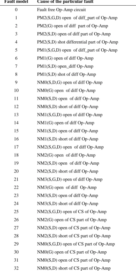
separately. In this way almost all fault models are designed by a fault number as shown in the Table 1. For example, fault 5 indicates that the Source (S), Gate (G), Drain (D) of the PMOS (PM1) are opened.
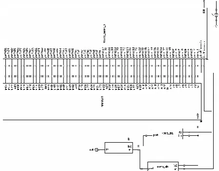
3. 3. Fault Injection and Comparison After fault modeling, each fault is injected and simulated sequentially by a multiplexer. The simulated outputs of the fault models are compared with the simulated output of fault free model. Here two comparators are used to check the fault model output with the upper and lower threshold of fault free one as shown in Figure 5.
TABLE 1. Fault Models due to different faulty nodes
Fault model Cause of the particular fault
0 Fault free Op-Amp circuit
1 PM2(S,G,D) open of diff_part of Op-Amp 2 PM2(G) open of diff part of Op-Amp 3 PM2(S,D) open of diff part of Op-Amp 4 PM2(S,D) shot differential part of Op-Amp 5 PM1(S,G,D) open of diff_part of Op-Amp 6 PM1(G) open of diff Op-Amp
7 PM1(S,D) open_diff Op-Amp 8 PM1(S,D) shot of diff Op-Amp 9 NM0(S,D,G) open of diff Op-Amp 10 NM0(G) open of diff Op-Amp 11 NM0(S,D) open of diff Op-Amp 12 NM0(S,D) short of diff Op-Amp 13 NM1(S,G,D) open of diff Op-Amp 14 NM1(G) open of diff Op-Amp 15 NM1(S,D) open of diff Op-Amp 16 NM1(S,D) short of diff Op-Amp 17 NM2(S,G,D) open of diff Op-Amp 18 NM2(G) open of diff Op-Amp 19 NM2(S,D) open of diff Op-Amp 20 NM2(S,D) short of diff Op-Amp 21 NM3(S,G,D) open of diff Op-Amp 22 NM3(G) open of diff Op-Amp 23 NM3(S,D) open of diff Op-Amp 24 NM3(S,D) short of diff Op-Amp 25 NM2(S,G,D) open of CS of Op-Amp 26 NM2(G) open of CS part of Op-Amp 27 NM2(S,D) open of CS part of Op-Amp 28 NM2(S,D) short of CS part of Op-Amp 29 NM0(S,G,D) open of CS part of Op-Amp 30 NM0(G) open of CS part of Op-Amp 31 NM0(S,D) open of CS part of Op-Amp 32 NM0(S,D) short of CS part of Op-Amp
Figure 3. Stuck at short model of an Op-Amp
Figure 4. Stuck at open model of an Op-Amp
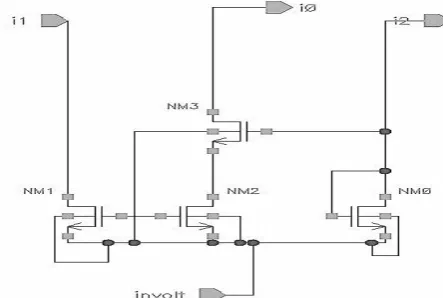
Figure 5. Circuit diagram of single fault injection for an Op-Amp
The threshold value is considered because in the analog circuit the output possesses a range of values depending upon the tolerance of electrical elements like a resistor, inductor, and capacitor. For the case of inverting Op-Amp two resistors, R1 and R2 having a tolerance of ±5% can vary the inverting gain (R2/R1). Accordingly we got a maximum output limit and minimum output limit.
4. POWER MINIMIZATION DURING TESTING
With respect to the changing trend of technology the transistor count increases within the chip. Therefore power density increases which results in temperature increment in the circuit and can burn the device. From the testing point of view, the testing power is nearly double to that of the normal mode of operation. This variation in power may change the temperature of the circuit and as a consequence the circuit performance is being affected. Therefore power management is also important for the proper functionality of the circuit. Scaling of technology node increases power-density more than expected. Though dynamic power is the major source of power dissipation but as technology scales down leakage power dominates over dynamic power dissipation. Leakage current is the major contributor of total power consumption in the integrated devices in today’s submicron technology. For example, in circuit of Figure 3 if the circled resistor is short circuited then high current will flow and during testing of stuck at short fault of this element leads to high power dissipation due to high current flow. This leads to leakage current during testing. Leakage reduction techniques are used to minimize leakage current [6].
Leakage reduction includes adding a sleep transistor between actual ground terminal and circuit ground (termed as the virtual ground) as described in [6]. In sleep mode to cut-off, the leakage path the sleepy transistor is turned off. High threshold sleep transistor is used that cuts-off Vdd from the circuit when no switching activity is going on. The circuit diagram for leakage reduction is shown in Figure 8. Here a NMOS is connected between virtual GND and actual GND.
In this testing, a current correlator can also be used to minimize the power dissipation. The work presented here is a type of structural testing of the Op-Amp based on the observation of the cross-correlation between the
Figure 6. Block diagram of testing circuit for all injected faults
output voltage and the power supply current as referred from [7]. In [7] current correlator circuit is used to minimize leakage current of a decoder circuit. The circuit’s power supply current (Idd) and the output signal (voltage, v), are taken for cross-correlation. Before the cross-correlation, the faulty signal is modeled as the sum of the good one and the deviation [8-11].
xF = xG + dx
The cross correlation can be expressed as V⊗I and is equal to: ) ) ( ) ( ))( ( ) ( ( 1 lim 2 / 2 / dt t dI t I t dv t V T I RV dd T T G dd G T F dd
F
(1)
The deviations of either or both V and Idd (dv and dIdd respectively due to defective behavior) are compressed or canceled out after the cross-correlation.
Considering VG(t) and
I
G(
t
)
dd as good responses, and VF(t) = VG(t) + dv(t) and
I
(
t
)
I
ddG(
t
)
F
dd
+ dIdd(t) as their respective faulty responses, the cross-correlationbetween
V
F(
t
)
andI
ddF gives:) ( ) ( ) ( )
(t RV dI t RdvI t RdvdI t I RV I RV dd G dd dd G G dd G F dd
F
(2)
In above case if the deviation terms are canceled then the correlation output will be equal to that of a fault-free one and the power dissipation will be as same as that of fault free power dissipation. For the above testing current correlator used as shown in Figure 7 and the testing circuit is shown in Figure 8.
In Figure 8, transistors are assumed to operate in the sub-threshold region.
)
( S D
G V V
KV S
DS e e e
L W I
I (3)
where, Is is the transistor’s specific current. VG , Vs , and VD are respectively the transistor’s gate, source, and drain voltages, K≈0.7 is the back-gate coefficient, and the voltages are given in units of the thermal voltage
(VT = kT/q ≈ 26 mV at 300ºK). From Figure 8 by
developing the sum of voltages in the Trans linear loop it can be shown that (−VGSNM1 + VGDNM2 –VGSNM3 +
VGSNM0 = 0), and assuming that all transistors except
NM2 are saturated, the output current can be derived as:
2 2 1 1 2 1 2 1 0 r I r I r r I I I (4)
r1 and r2 are transistors dimension ratio where: 1 1 2 2 1 L w L w r 0 0 3 3 2 L w L w r
voltage V. I0 is converted into an integrated output voltage (
d d I V
V
) that is:0
r h I V
h I V V
dd g
dd g I
V d d
(5)
where the transconductance gain g is defined by I1, r1 and V, the current gain h is defined by I2 , r2 and Idd . r0 is the correlator’s output transresistance.
Fault coverage The simulated output like output voltage, gain and average power has been checked with the fault-free output. Fault coverage is calculated for individual parameters using the formula:
Fault coverage is expressed in percentage. Fault coverage x % means out of 100 possible faults, x number of faults can be tested for a circuit and (100-x) numbers of faults cannot be detected though those are defective. Therefore more fault coverage gives better testing.
5. RESULT AND ANALYSIS
As discussed above in section 3 an Op-Amp is taken as CUT for analog testing. A two stage Op-Amp is designed in Cadence Tool using 45nm technology as per the specifications discussed in section 3. The circuit is designed with out making it an oscillator in order to make the testing circuit less complex. As discussed above, first different fault models are designed in Cadence Tool. Then the simulation outputs are saved in the LUTs after fault injection. Here output voltage, dc gain and average power are taken as testing parameters. After simulation of the fault free circuit the outputs are stored in different files with respect to time (here time is sampled to finite intervals in order to minimize execution time) using C-programming. The files are the LUTs. The data stored in .txt files are considered as the references for fault free circuit.
Figure 7. Current correlator circuit
Figure 8. Testing Op-Amp circuit with current correlator
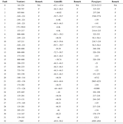
32 faults are modeled for testing. The measured output of the particular device to be tested is then compared with the fault free output which is already stored in .txt file. If the output matches with the referred value, then we can say that our test passes (i.e circuit is fault free w.r.t that parameter) otherwise test fails (circuit is faulty w.r.t that parameter). Likely the target circuit output is then compared with 32 fault results sequentially and when there is an equality found then the testing circuit has a particular fault according to the matching result. For example from Table 2 it is observed that if after simulaton of an Op-Amp the output voltage is in the rage of 789~797mv, then it is as per entry in row no. 3 and fault no. 1(PM2(S,G,D) open of diff_part of Op-Amp) of the LUT (Table 2) and the fault is in PMOS i.e. in PM2 of the differential pair of the Op-Amp circuit but if the output volatge would be in the range of (161-224) then there is no fault in terms of output voltage. But sometimes it may happen that the faulty output matches with the fault free output as in case of fault model 6 (8th row of Table 2). As a result 100% fault coverage is not achieved for output voltage but this kind of demerits can be recovered by testing the faults according to their priority levels.
Table 2 is the Look up Table for parameters like output voltage, gain and average power. Here, P and F indicate that particular test passes or fails respectiely. The simulation outputs of both fault free and faulty circuit have been stored prior to the testing process.
Table 3 is the Look up Table for the same parameters like Table 1 have been considered. In the second case the power minimization technique - sleepy stack and current correlator has been added to the normal testing circuit to reduce the power during testing. From Table 2 and Table 3 the fault coverage has been calculated.
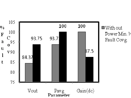
OBIST method is 84.375%. In the proposed method fault coverage of output voltage has been enhanced to 93.75% in power minimization technique as compared to that of 84.375% (normal mode). More coverage gives a better testing result. Here fault coverage for average power is better than other two parameters. Here only 32 fault models have been designed if no. of fault models are increased then fault coverage will also increase. From this proposed method it is analyzed that: i. Though in OBIST method we can increase the fault
coverage by injecting more no. of faults, the exact fault coverage can be calculated by following an algorithmic approach.
ii. It has better fault coverage than the OBIST method. iii. For a faulty block here we can predict the particular faulty node.
iv. Testing power is also minimized to some extent using sleepy stack and current correlation method. The percentage of power saving for each fault is shown in Figure 9.
TABLE 2. Look up Table of fault simulation without power Minimization
Fault Vout(mv) Remark Gain(dB) Remark P(avg)(µw) Remark
0 161-224 NA -43.1 ~-43.4 NA 212.9-213.5 NA
1 789-797 F -46.3~-46.3 F 315-325 F
2 855-864 F ~-46.02 F 237-248 F
3 -249~-221 F -59.7~-59.7 F 3769-3774 F
4 -249..-221 F -6.4K F ~139 F
5 -249..-221 F -46.3~-46.3 F ~141 F
6 175~198.8 P -6.4k F 217.7~218. F
7 153~217 F -6.4k F 214.6~215 P
8 800~808 F -58.3 ~-59.3 F 323-333 F
9 -249~-221 F ~46.36 F 56.1~56.4 F
10 167-211 P -46.3~-59.6 F 218.7~219 F
11 -249~-221 F -59.7~ -59.7 F 56.3~56.4 F
12 800~808 F -59.39 F 348~358 F
13 800~808 F -72.7~-58.7 F 320~330 F
14 173~192 P -46.3~-46.3 F ~215 P
15 800~808 F ~-58.74 F 320~330 F
16 206~233 F -46.3~-46.3 F ~21 F
17 206~233 F -46.3~-46.3 F ~21 F
18 735~741 F -46.3~-46.3 F ~125 F
19 303~338 F -46.3~-46.3 F 151~153 F
20 -348~-314 F ~46.36 F ~6712 F
21 -182~-136 F -64.6~-66.6 F 2865~6231 F
22 174~202 P ~46.33 F ~218 F
23 -171~-126 F -64~-66.9 F ~81080 F
24 635~665 F ~-46 F 104~108 F
25 135~201 F ~46.36 F 217~218 F
26 113~131 F ~46.36 F 244~245 F
27 -175~-165 F -46.21 F ~125 F
28 135~201 P -46.35 F 217~218 F
29 205~251 F -46 F ~134 F
30 114~167 F -46.23 F 178~179 F
31 139~193 F -46 F 125.5 F
TABLE 3. Look up Table of fault simulation with power Minimization.
Fault Vout (mv) Remark P(avg)(µw) Remark Gain(dB) Remark
0 884~897 NA 191.5-194 NA -59.75 ~ -59.8 NA
1 991.8~992.4 F 313-323 F -59.73~-59.77 P
2 994~995 F 239-250 F -59.22 F
3 922~923 F 667-671 F -59.73~-59.77 F
4 872~873 F 176-177 F -6.4k F
5 872.8~873.3 F 178~179 F -59.73~-59.77 F
6 882~887 F 207~210 F -6.4k F
7 879-890 F 202~206 F -6.4k F
8 992.4~992.9 F 321-332 F -72.03~-72.66 F
9 871.6~871.8 F 97.3-98.6 F -59.83 F
10 ~872 F 211~221 F -59.74~-59.78 F
11 872.8~873.2 F 97.4~98.6 F -46.34~-46.36 F
12 992.5~993 F 349~359 F -59.33~72.7 F
13 992.4~992.9 F 319~329 F -72.69~-72.05 F
14 881~886 F 202~206 F -59.77~-59.74 F
15 992.4~992.9 F 319~329 F -72.69~-72.06 F
16 ~873 F 180~181 F ~59.77 P
17 913~922 F 180~181 F ~59.77 P
18 880~891 F 152~153.5 F ~59.77 P
19 915~923 F 153~154 F -46.34~59.77 F
20 872~886 F 552~555 F -~59.84 F
21 ~987 P 720~730 F -95~-93 F
22 880~891 F 208~211 F ~59.7 F
23 ~987 P 730 F -94~96 F
24 ~984 F 113~120 F ~-59.2 F
25 ~887 F 201~206 F ~59.8 F
26 ~887 F 164~167 F -59.9 F
27 873-875 F 155~157 F -59.55~-59.5 F
28 874 F 201~206 F -59.77~-59.8 F
29 ~875 F 133~165 F ~-59.23 F
30 876 F ~168.5 F -59.6 F
31 887-883 F 1~25 F -46 F
32 ~972 F 721~728 F -106~112 F
TABLE 4. Fault coverage
Parameter Total Faults
Without power Min. With power Min.
Detected % Coverage Detected % Coverage
Vout 32 27 84.375 30 93.75
Pavg 32 30 93.75 32 100
Figure 9.% Power saving
Here power minimization is taken into priority because it has been observed from Look up Table 2 that in case of some particular faults the circuit average power reaches to a high value which is hundred times greater than that of a normal circuit (consider the case of fault no 20, 23 in Table 2) which can burn the testing kit or increase the temperature of the testing kit which would lead to a wrong testing. But by using the power minimization technique (as observed from Table 3) like sleepy transistor and current correlator simultaneously the power has been minimized that is made comparable to that of a normal circuit (consider the Look up Table 3 for fault 20 and 23).
In this proposed method three parameters are considered as testing parameters which has increased the quality of testing as compared to OBIST method where only one parameter is being tested. Multiple parametric testing is more better because it may also happen that one circuit is fault free w.r.t one parameter and could be faulty w.r.t other parameters.Therefore this technique has more accuracy than OBIST. In OBIST only one fault is being tested at once by comparing the outputs, but in this proposed method all the possible faults are being tested sequentially. Previously there was no such power reduction techniques are being applied which now one of the major issues is found during testing. Instead of comparing infinite points here no. of testing points are reduced by sampling the simulation time into finite number of time instants. Here LUT based programming approach improves hardware complexity and reduces testing time.
In this paper testing is being carried out by taking only one fault at a time depending upon the fault model. Multiple fault detection can be possible. For that fault models have to be designed accordingly. Results of all combinational faults can be stored in the LUT and while testing responses can be compared with values stored in the LUT as reference. It depends on the controllability and observibility of fault testing (i.e No. of fault model, priority order of testing, classification of faults).
In the proposed work good testability and power reduction during testing are achieved after sacrificing additional chip area due to the addition of sleepy transistors and current correlator. However, the increase in area has been compensated by the increase in testability and low power dissipation during testing. Reduction of power during testing is essential and here it is minimized and the drawbacks of power dissipation is resolved to get better testability. If we concern about area then it is apparently optimized as:
i. In previous work(OBIST), one extra circuit (fault free circuit) is being taken for comparison, but here the responses of a fault free circuit is being stored once and being compared during testing either for a single CUT or multiple CUTS in SOCs. In this work for power reduction additional 5 transistors are used which would occupy lesser area if CUT is a bigger circuit (as for OBIST testing, total transistors=2*No. of transistors used in CUT).
ii. If we make our testing circuit (except CUT) as external then it would be one time fabrication process for testing which would save cost, area and time. iii. With respect to changing technology i.e. suppose we are jumping from 90nm technology to 45nm technology, obviously we are decreasing the size of the transistor. Therefore within the same area we can fabricate extra transistors (by proper placement and routing).
iv. From Figure 10 it is observed that the fault coverage of a parameter is improved (fault coverage has been improved from 84% to 93% for Vout) which proves a better testability.
v. Here area can be compromised if we consider the advantage of the testing i.e. 1. fault coverage improvement and 2. finding the particular fault location of CUT.
6. CONCLUSION
Fault Coverage of OBIST method is 84.37% without power reduction technique and that is improved to 93.45% by the proposed programming approach along with the power reduction technique. Here along with the improved fault coverage, the particular faulty node can be detected. In OBIST method the faults are injected one by one manually but in programming or algorithmic approach all faults are tested sequentially according to the algorithm and the analog circuit is tested with exact fault coverage within a lesser time. It has been also found that among all parametric testing; average power and dc gain test has shown better fault coverage than output voltage testing for same number of fault models. During testing power minimization techniques are applied. Sleepy stack approach along with a current correlator together able to reduce the testing power of the circuit upto 84%.
7. REFERENCES
1. Arabi, K. and Kaminska, B., "Oscillation built-in self test (OBIST) scheme for functional and structural testing of analog and mixed-signal integrated circuits", in Test Conference, Proceedings., International, IEEE, (1997), 786-795.
2. Dhare, V. and Mehta, U., "SAF analyses of analog and mixed signal vlsi circuit: Digital to analog converter", International Journal of VLSI Design & Communication Systems (VLSICS), Vol. 6, No. 3, (2015).
3. Roh, J. and Abraham, J. A., "A comprehensive signature analysis scheme for oscillation-test", IEEE Transactions on Computer-Aided Design of Integrated Circuits and Systems, Vol. 22, No. 10, (2003), 1409-1423.
4. Arbet, D., Stopjakova, V., Majer, L., Gyepes, G. and Nagy, G., "New obist using on-chip compensation of process variations toward increasing fault detectability in analog ICs", IEEE Transactions on Nanotechnology, Vol. 12, No. 4, (2013), 486-497.
5. H. Meharkure and Gourkar, S., "Fault testing of analog circuits using combination of oscillation based built-in self-test and quiescent power supply current testing method", IJAIEM, Vol. 2, No. 12, (2013).
6. Oza, A. and Kadam, P., "Techniques for sub-threshold leakage reduction in low power cmos circuit designs", International Journal of Computer Applications, Vol. 97, No. 15, (2014). 7. Winstead, C. J. and Schlegel, C ,.Low-voltage cmos circuits for
analog decoders, (2008), Google Patents.
8. da Silva, J. M., Matos, J. S., Bell, I. M. and Taylor, G. E., "Cross-correlation between iDD and vOUT signals for testing analogue circuits", Electronics Letters, Vol. 31, No. 19, (1995), 1617-1618.
9. Lin, X.-n., Liu, P. and Malik, O., "Studies for identification of the inrush based on improved correlation algorithm", IEEE Transactions on Power delivery, Vol. 17, No. 4, (2002), 901-907.
10. Bi, D., Zhang, X., Yang, H., Yu, G., Wang ,X. and Wang, W., "Correlation analysis of waveforms in non-saturation zone based method to identify the magnetizing inrush in transformer", in 2006 International Conference on Power System Technology, IEEE, (2006), 1-6.
11. Etumi, A., Anayi, F., Fahmy, A. and Eldukhri, E., "Auto-cross correlation coefficients used for detecting an internal fault in three phase transformer", in 2014 16th International Conference on Harmonics and Quality of Power (ICHQP), IEEE, (2014), 370-374.
Look up Table Based Low Power Analog Circuit Testing
TECHNICALNOTE
L. Maharana, T. Sarkar, S. Nath Pradhan
Department of Electronics and CommunicationEngineering, National Institute of Technology Agartala, Tripura, India
P A P E R I N F O
Paper history: Received 07February2016 Received in revised form 14July 2016 Accepted 14July 2016
Keywords:
Oscillation-based Built in Self-test (OBIST) Look up Table (LUT)
Analog Testing Operational Amplifier Fault Coverage Low Power Current Correlator
هديكچ
.تسا ٌذض داُىطیپ هیياپ ناًت گًلاوآ نًمزآ زا یضير ٍلاقم هيا رد تاواسًو یاىثم رت یويرد یوًمزآ دًخ شير یاج ٍت
(OBIST)
باختوا ليذج کي یاىثم رت هیياپ ناًت صيامزآ ًٌیض
(LUT)
دًض اذیپ بًیعم راذم ات تسا ٌذض ٍئارا ريداقم ي
ةیع لحم ي ٌذض یحارط تسا گًلاوآ یاَ راذم یدایىت یاىت گىس ٍک یتایلمع ٌذىىک تيًقت کي .ددرگ صحطم سیو راذم رد
ذصرد .تسا ٌذض ٍتفرگ راکت صيامزآ رًظىم ٍت دًجي
صخطم اَ ةیع یزاس ٍیثض ي یزاس لذم ،ةیع لامعا زا ذعت اَ ةیع
.تسا ٌذض زا صیت ات ةیع صیخطت 39
د یىیت صیپ ي ٌذض لصاح % گًلاوآ یاَ نًمزآ ٍک اجوآ زا .دًض یم سیو یرتطیت ذص ر
ناًت یزاس ٍىیمک یاَ شير یضعت ،دراد ٌارمَ ار ناًت فلاتا صلاچ ذىوام
sleepy stack
ذىيآرف رد نايرج یگتسثمَ ي
صيامزآ ناسیم ات یواًت صَاک یسررت هيا رد .تسا ٌذض ٍتفرگ راکت 48
.تسا ٌذمآ تسذت اَ صيامزآرد %