Delay Estimation of Fast Test Pattern Generator
(TPG) using Ausim L 2.3
P. Malini T. Poovika
PG Scholar PG Scholar
Department of Electronics and Communication Engineering Department of Electronics and Communication Engineering SNS College of Technology, Coimbatore -35,India SNS College of Technology, Coimbatore -35,India
P. Shanmugavadivu I. Rinisha Prem Priya
PG Scholar PG Scholar
Department of Electronics and Communication Engineering Department of Electronics and Communication Engineering SNS College of Technology, Coimbatore -35,India SNS College of Technology, Coimbatore -35,India
G. Naveen Balaji Assistant Professor
Department of Electronics and Communication Engineering SNS College of Technology, Coimbatore -35,India
Abstract
This paper attempts to show the survey on Test pattern generator (TPG) of a 28bit LFSR with Gate delay, propagation delay, and total number of gates are listed. The circuits were built in .asl file and simulated using AUSIM L2.3. The operation of digital logic simulator called the Auburn University Simulator (AUSIM) is described. The AUSIM version L2.3 besides providing simulation of non-hierarchial circuit descriptions it also provides area and performance audits of the cell.
Keywords: Linear Feedback Shift Register (LFSR), Test Pattern Generator (TPG), gate delay, propagation delay, AUSIM L2.3
________________________________________________________________________________________________________
I. INTRODUCTION
The analysis of total number of gates, gate delay and propagation delay for the Test pattern generator (TPG) of a 28bit LFSR. The connection of AND, NAND, OR, NOR in the combinational circuit are described. The Test pattern generator (TPG) circuit has the maximum gate delay and propagation delay of 11 and 64.
II. AUSIM OVERVIEW
Logic simulation has become essential in ensuring that a digital design is correct prior to actual implementation of the hardware. The correctness of a digital logic circuit is done through a simulation process called as design verification. One of the inputs to any logic simulation tool is a description of the digital design in some hardware description language. The hardware description language for Auburn University Simulator. AUSIM is the Auburn Simulation Language (ASL).In addition to providing simulation for debugging and verifying digital designs, AUSIM provides audits which can aid in debugging a circuit or in analyzing a circuit in terms of area and performance metrics. This version of AUSIM(version L2.3) simulates digital circuits described as elementary logic gates (AND, OR, NOT,NAND, and NOR gates).
III. TEST PATTERN GENERATOR
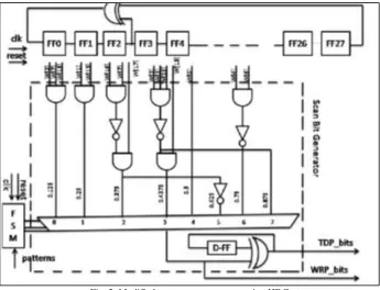
Fig. 2: Modified test pattern generator using HDC
A weight is selected through the select lines of the MUX and the bit sequence is fed to one of the inputs of the XOR gate; the other input line of the XOR gate is the output of the D flip-flop. As soon as a weight is selected the transition at the output of the XOR gate is being controlled by the corresponding bit sequence. A 1 in the bit sequence will produce a transition at the output of the XOR gate and a 0 will produce no transition. Sothe final transition density in the bit stream that is being obtained at the output of the XOR gate will have the similar weight (i.e., the probability of a transition to occur) as the weight that is selected from the MUX.
IV. AUSIM SOFTWARE DESCRIPTION
The AUSIM process involves two input files namely: ASL (Auburn Simulation Language) file and a vector file. These input files can be generated by any text editor program but these files should be saved as text files. The ASL description comprises of two statements namely circuit statement and component statement. The circuit statement for a 4 BIT LFSR circuit can be given by the syntax as:
ckt: mux in: a b c d clk s out: r3 ; not: x in: s out: sn ;
and: a1 in: a sn out: a1 ; and: a2 in: r3 s out: a2 ; or: o1 in: a1 a2 out: z ; dff: f in: clk z out: r ; and: a3 in: b sn out: a3 ; and: a4 in: r s out: a4 ; or: o2 in: a3 a4 out: z1 ; dff: f1 in: clk z1 out: r1 ; and: a5 in: c sn out: a5 ; and: a6 in: r1 s out: a6 ; or: o3 in: a5 a6 out: z2 ; dff: f2 in: clk z2 out: r2 ; and: a7 in: d sn out: a7 ; and: a8 in: r2 s out: a8 ; or: o4 in: a7 a8 out: z3 ; dff: f3 in: clk z3 out: r3 ;
In the component statement the name of the component (NOT,AND,OR,NAND,NOR) is used as the keyword instead of the “CKT” keyword. Every gate is given with unique names. The vector file is an input stimulus file which specifies the input patters to be applied to the circuit. The vector file can be represented by the syntax as:
111000 111010 111001 111011 100000 100010 100001 100011 110100 110110 110101 110111 011000
V. SIMULATING WITH AUSIM
In order to access the AUSIM L2.2, AUSIM executable (ausim.exe) is copied into the directory that contains the ASL and vector files for the simulation. From the Windows Explorer or My Computer, double click the ausim.exe icon in the directory file. The AUSIM window should appear. The AUSIM window consists of three main areas:
1) The Input/output File Control section at the top left hand side of the window. 2) The Circuit Statistics list at the top right hand side of the window.
3) The Process and Simulate buttons and Status dialog area at the bottom of the window.
VI. ENTERING FILE NAMES
The first step upon entering AUSIM is to specify the names of the input and the output files. These can be entered individually by moving the cursor to the appropriate file name box, clicking the left mouse button, and entering the full name of the associated file name. The input files consists of two main files namely ASL file and the input vector (or VEC) file. Similarly the output file comprises of the audit (or AUD) file and simulation results (or OUT) file. The default asl and vector file names have been automatically chosen by typing the file prefix name into the text box which will appear in the top center of the Input/output File Control section.
As the file prefix is typed in the “prefix” textbox, the names of the various input and output files appear in their respective text boxes with their default file suffix. The default naming convention used allows all files to be associated with a given circuit that have the same prefix. It can be easily found in the directories containing multiple versions of a circuit. The default naming convention used in the ASL and VEC files must be saved correspondingly and is named with the correct file suffix (“.asl” and “.vec”, respectively).
VII. PROCESS OF .ASLFILE
The ASL file must be processed by AUSIM software after the names of the files have been specified, this action can be performed by clicking the Process button. The result of the ASL file includes the following steps:
1) Check to see that the ASL file exists. In case of failure to find the file will result as a “can’t find ASL file”. 2) If there are any syntax errors in the ASL description check the syntax of the ASL file.
3) It will result in a message “Syntax Errors in ASL file - check 'ausim_errs.txt' for any details”. 4) Count the number of gates driven by signal nets the internal data structures for subsequent simulation. 5) The audit of the circuit is performed to check for any of the connectivity problems.
6) Problems found will result in a status box message – “Circuit errors encountered - check 'ausim_errs.txt' and AUD file. The audit of the circuit looks for problems such as:
1) unconnected gate inputs (nets with no driving source).
2) unconnected outputs (nets with no loads, other than primary outputs). 3) When multiple gates drives the same signal net.
4) duplicate gate names.
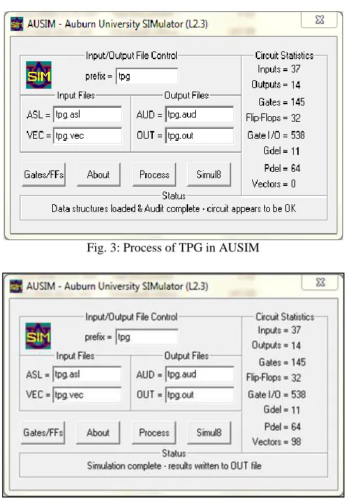
VIII. PROCESS OF TPG
Fig. 3: Process of TPG in AUSIM
Fig. 4: Simulation of TPG in AUSIM
IX. PROGRAM FOR TPG
The asl file program for the 28 bit Linear Feedback Shift Register (LFSR) of a Test Pattern Generator (TPG) is as follows. This is example program of the 10 bit LFSR. The following Program can be extended for the 28 bit LFSR design.
ckt: mux in: a b c d e e1 g h i j k l m n o p q e2 e4 t u v w x y e3 t1 t2 clk s clk1 se x3 x4 x5 se1 h15 out: r27 p0 p1 p2 p3 r p5 p6 x2 x22 x23 x24 u1 tdp ;
dff: f4 in: clk z4 out: r4 ; and: a11 in: e1 sn out: a11 ; and: a12 in: r4 s out: a12 ; or: o6 in: a11 a12 out: z5 ; dff: f5 in: clk z5 out: r5 ; and: a13 in: g sn out: a13 ; and: a14 in: r5 s out: a14 ; or: o7 in: a13 a14 out: z6 ; dff: f6 in: clk z6 out: r6 ; and: a15 in: h sn out: a15 ; and: a16 in: r6 s out: a16 ; or: o8 in: a15 a16 out: z7 ; dff: f7 in: clk z7 out: r7 ; and: a17 in: i sn out: a17 ; and: a18 in: r7 s out: a18 ; or: o9 in: a17 a18 out: z8 ; dff: f8 in: clk z8 out: r8 ; and: a19 in: j sn out: a19 ; and: a20 in: r8 s out: a20 ; or: o10 in: a19 a20 out: z9 ; dff: f9 in: clk z9 out: r9 ; ...
X. SIMULATION RESULTS
Area Analysis
Number of primary inputs: Pi= 37 Number of primary outputs: Po= 14 Number of gates: G= 145 Number of flip flops: FF= 32 Number of gate I/O pins: Gio= 538 Gate type and number of uses: AND: 92
OR: 38 NOT: 15 DFF: 32
Loading and Delay Estimation r27 1 DFF 3=2+1 Output p0 1 AND 3=2+1 Output p1 1 AND 3=2+1 Output p2 1 AND 3=2+1 Output p3 1 AND 3=2+1 Output r 2 DFF 4=2+2 Output p5 1 NOT 2=1+1 Output p6 2 NOT 3=1+2 Output x2 2 NOT 3=1+2 Output x22 5 DFF 7=2+5 Output x23 5 DFF 7=2+5 Output x24 5 DFF 7=2+5 Output u1 2 OR 10=8+2 Output tdp 1 OR 3=2+1 Output sn 28 NOT 29=1+28 Timing Path Analysis
path= r27(FFin)clk: Gdel=0, Pdel=28
path= r27(FFin)z27->a55->t2: Gdel=2, Pdel=7 path= r27(FFin)z27->a55->sn->s: Gdel=3, Pdel=64 path= r27(FFin)z27->a56->r26: Gdel=2, Pdel=7 path= r27(FFin)z27->a56->s: Gdel=2, Pdel=35 path= p0->r15: Gdel=1, Pdel=6
. .
path= r25(FFin)z25->a51->sn->s: Gdel=3, Pdel=64 path= r25(FFin)z25->a52->r24: Gdel=2, Pdel=7 path= r25(FFin)z25->a52->s: Gdel=2, Pdel=35 path= r26(FFin)clk: Gdel=0, Pdel=28
path= r26(FFin)z26->a53->t1: Gdel=2, Pdel=7 path= r26(FFin)z26->a53->sn->s: Gdel=3, Pdel=64 .
.
. path= x22(FFin)l1->t4->x15->x14->x11->x10->x7->x4: Gdel=7, Pdel=28 path= x22(FFin)l1->t4->x15->x14->x11->x8->x5: Gdel=6, Pdel=24 .
. .
path= tdp->h13->h12->u1->h4->p3->x2->q2->y15->r3: Gdel=9, Pdel=37 path= tdp->h13->h12->u1->h4->p3->x2->q2->y15->r5: Gdel=9, Pdel=37 .
.
path= h10(FFin)h18->h17->tdp->h13->h12->u1->h4->p3->x2->q2->y15->r3: Gdel=11, Pdel=43 path= h10(FFin)h18->h17->tdp->h13->h12->u1->h4->p3->x2->q2->y15->r5: Gdel=11, Pdel=43 path= h10(FFin)h18->h17->tdp->h13->h12->u1->h4->p3->r15: Gdel=8, Pdel=35
path= h10(FFin)h18->h17->tdp->h13->h12->u1->h5->x22: Gdel=7, Pdel=34 path= h10(FFin)h18->h17->tdp->h13->h12->u1->h5->v2->x23: Gdel=8, Pdel=39 path= h10(FFin)h18->h17->tdp->h13->h12->u1->h5->v3->x24: Gdel=8, Pdel=39 path= h10(FFin)h18->h17->tdp->h13->h12->u1->h5->r: Gdel=7, Pdel=31 path= h10(FFin)h18->h17->tdp->h13->h12->u1->h6->x22: Gdel=7, Pdel=34 .
.
path= h10(FFin)h18->h17->tdp->h14->u1->h8->x2->q2->r25: Gdel=8, Pdel=35 path= h10(FFin)h18->h17->tdp->h14->u1->h8->x2->q2->y15->r3: Gdel=9, Pdel=38 path= h10(FFin)h18->h17->tdp->h14->u1->h8->x2->q2->y15->r5: Gdel=9, Pdel=38 path= h10(FFin)h18->h17->tdp->h14->h11->h10: Gdel=5, Pdel=16
path= h10(FFin)h18->h17->se1: Gdel=2, Pdel=8 path= h10(FFin)clk1: Gdel=0, Pdel=4
Worst Case: Gdel=11, Pdel=64
XII. SUMMARY AND CONCLUSION
In this paper, Gate delay and Propagation delay of the Test pattern generator (TPG) of a 28bit LFSR are found with the help of the AUSIM L2.3.Based on the simulation results the gate delay is found as 11 and propagation delay is calculated as 64 for the Test pattern generator (TPG) of a 28bit LFSR.
REFERENCES
[1] S. Kim and M. C. Papaefthymiou, “Single-phase source-coupledadiabatic logic,” Proc. Int. Symp. Low-Power Electronics and Design, pp. 97-99, Aug. 1999.
[2] S. Zhao and K. Roy, “Estimation of switching noise on powersupply lines in deep sub-micron CMOS circuits,” 13th International Confserence.VLSI Design,
pp. 168 –173, Jan. 2000.
[3] D. Gizopoulos, N. Krantitis, A. Paschalis, M. Psarakis, and Y. Zorian, (May 2000) ―Low Power/Energy BIST Scheme for Datapaths,‖ in Proc. IEEE 18th
VLSI Test Symp., , pp. 23–28.
[4] S. Wang, (Dec 2002) ―Generation of Low Power Dissipation and High Fault Coverage Patterns for Scan- Based BIST,‖ in Proc. International Test Conf., ,
pp. 834–843
[5] M.C.B. Osorio, C.A. Sampaio, A. I. Reis, R.P. Ribas., etc.al. “Enhanced 32-bit Carry Look ahead Adder using Multiple Output Enable-Disable CMOS
Differential Logic”. SBCCI, pp. 181-185, 2004.
[6] S.M.Kang, Y.Leblebici,“CMOS Digital Integrated Circuits: Analysis and Design” Tata McGraw-Hill, 2003. [5] S. Samanta “Adiabatic Computing” a
contemporary review, “4th international conference on computer and devices for communication: codec 09”, 2009.
[7] Jagannathsamanta, Mosamhalder, Bishnu Prasad De “Performance analysis of high speed low power cerry look ahead Adder” International journal of soft
computing and Engineering (IJSCE) ISSN: 2231 – 2307, Volume -2, Issue-6, Jan-2013.
[8] Amita, “Design and analysis of carry look ahead adder using CMOS technique” IOSR journal of electronics and communication Engineering:
ISSN:2278-2834, vol-9,issue2(MAR-APR) 2014 pp-92-95.
[9] G. Naveen Balaji, S. Karthikeyan, M. Merlin Asha “ 0.18μm CMOS Comparator for High-Speed Applications” International Journal of Trend in Scientific
Research and Development, Vol. 1, No. 5, pp: 671-674, ISSN 2456 - 6470
[10] G. Naveen Balaji, K. Saravanan, R. Poorani, T. Vishnu Priya, R. Reka Raj “Advanced Security System using PIC through Bluetooth” International Journal
of Trend in Scientific Research and Development, Vol. 1, No. 5, pp: 675-685, ISSN 2456 - 6470
[11] G. Naveen Balaji, N.V. Hari Suriya, S. Anand Vikash, S. Arun Kumar, R. Arun, “Gasoline Purity Meter Using Peripheral Interface Controller for Automobile
Applications” International Journal of Engineering and Technical Research (IJETR), Vol. 7, No.10, pp:46-55, ISSN: 2321-0869
[12] G. Naveen Balaji, S.Chenthur Pandian, “Design for Testability of Kipbond Logic” “Perspectivas em Ciência da Informação” (Annexure - I), School of
Information Science of the Federal University of Minas Gerais (UFMG), Vol. 22, No. SP.01, pp: 261-284, ISSN 1413-9936
[13] G. Naveen Balaji, V. Nandhini, S. Mithra, N. Priya , R. Naveena, “IOT Based Smart Crop Monitoring in Farm Land”, Imperial Journal of Interdisciplinary
Research (IJIR) Vol. 4, No. 1, pp: 88-92, ISSN: 2454-1362
[14] G. Naveen Balaji, N. V. Hari Suriya, “Effective Badminton Coaching Schema using PIC16F887 Microcontroller”, International Journal of Trend in Scientific
Research and Development, Vol. 2, No. 2, pp: 178 – 182, ISSN 2456 - 6470
[15] G. Naveen Balaji, S. Chenthur Pandian, “Power Analysis of a Transmission Gate based Scan Flip Flop”, International Journal of Engineering Research in
Electronics and Communication Engineering (IJERECE) Vol 4, Issue 11, November 2017, pp:48-53, ISSN: 2394-6849
[16] P.Malini, T.Poovika, P.Shanmugavadivu, G.Naveen Balaji, “Design of High Speed 8 Bit Carry Look Ahead Logic for Arithmetic Operations”, International
Journal of Engineering Research in Electronics and Communication Engineering (IJERECE) Vol 4, Issue 12, December 2017, pp:59-62, ISSN: 2394-6849
[17] G. Naveen Balaji, D.Rajesh, S. Sowmya, M. Subashini, P. Suryaprabha, “Power Analysis of an Approximate adders under various interpolation factors for
DSP Applications”, International Journal of Engineering and Technical Research, Vol. 8, Issue 1, January 2018, pp: 379 – 383, ISSN: 2321-0869
[18] G. Naveen Balaji, V. Nandhini, S. Mithra, N. Priya , R. Naveena “Advanced Crop Monitoring using Internet of Things based Smart Intrusion & Prevention
in Agricultural Land” International Journal of Trend in Scientific Research and Development, Vol. 2, No. 2, pp: 1348-1352, ISSN 2456 – 6470
[19] Merlin Asha. M, G. Naveen Balaji, S. Mythili, A. Karthikeyan, N. Thillaiarasu, “An Efficient Brain Tumor Detection Algorithm based on Segmentation for