Themed Section: Science and Technology
A Sepic based AC-DC Convertor using FOPID Controller
Akhib Khan Bahamani*1, Dr. G. Venkateswarlu2
*1Assoc. Professor, Department of Electrical and Electronics Engineering, Narayana Engineering College,
Nellore, Andhra Pradesh, India
2Professor and Head, Department of Electrical and Electronics Engineering, Narayana Engineering College,
Nellore, Andhra Pradesh, India
ABSTRACT
This paper presents “A Sepic based AC-DC Convertor using FOPID Controller” is composed of a low-cost, reduced-switch, three-phase ac–dc buck–boost converter is conventional circuit is proposed. The converter can operate with input power factor correction and is suitable for applications where a converter needs to operate over a wide range of input ac voltages and/or produce a wide range of output dc voltages. To solve this problem SEPIC converter with ripple-free input current is proposed. In the proposed converter, the input bridge diode is removed and the conduction loss is reduced. In addition, the input current ripple is significantly reduced by utilizing an additional winding of the input inductor and an auxiliary capacitor. Similar to the conventional PFC SEPIC converter, the input current in a switching period is proportional to the input voltage and near unity powers achieved. The operational principles, steady-state analysis, and design equations of the proposed converter are described in detail.
Keywords: FOPID- Fractional order proportional Integral and derivative SEPIC- Single- Ended Primary-Inductor Converter PFC- Power factor correction
I.
INTRODUCTION
According to the demand on high efficiency and low Harmonic pollution, the active power factor correction (PFC) circuits are commonly employed in ac–dc converters and Switched - mode power supplies. Generally, these kinds of converters include a full-bridge diode rectifier on an input current path so that conduction losses on the full-bridge diode occur and it will be worse especially at the low line. To overcome this problem, bridgeless converters have recently been introduced to reduce or eliminate the full-bridge rectifier, and hence their conduction losses. A bridgeless boost converter is widely used in advantages of reduced input current ripple, but its output voltage should be higher than the peak voltage of the Inge.
II.
THE PROPOSED SEPIC CONVERTER
SYSTEM
Single- Ended Primary-Inductor Converter (SEPIC) is a DC-DC converter. It gives output voltage greater than, less than, or equal to that of the input voltage. The output of the SEPIC converter is controlled by the duty cycle of the semiconductor devices. SEPIC provides the input-to-output gain, thus making it popular in battery-powered systems. Unlike buck-boost converter, it has non-inverting output. This is achieved by using a series capacitor to couple energy from the input to the output.
capacitor, the capacitor should have high capacitance and current handling capability.
III. DESIGN AND WORKING PRINCIPLE OF
SEPIC CONVERTER
Figure 1 SEPIC Converter.
The circuit diagram of the SEPIC converter is shown in Figure 1. A SEPIC converter has two pairs of undamped complex poles, compared with other PFC converters, such as fly back converters and boost converters. It is less popular topology for PFC converter design since the control is not simple. Also due to the complexity of control, it is suitable only for very slow varying applications.. The output voltage is not necessarily limited by its input voltage. Furthermore, SEPIC PFC converter does not require an additional DC-DC stage for LED applications. Input current ripple can also be reduced by using two wound inductors. Thus power loss due to current ripple can be reduced.
The working of the SEPIC converter is explained as follows:
When the switch S is turned ON, the inductor L1 is charged from the input voltage source Vin. Meanwhile the inductor L2 takes energy from the capacitor C2. The capacitor C2 supplies the load. As seen from the discussion, both L1 and L2 are disconnected from the load. This makes the control characteristics complex. When the switch is turned OFF L1 charges C1 and also supplies current to the load. L2 is also connected to the load. The output capacitor C2 has a pulse of current during the OFF time, making SEPIC converter noisier than a buck converter while the input current is non-pulsating.
The SEPIC converter is designed for power factor correction and voltage control at DC link for a VSI fed PMBLDC motor drive. The design equations for the output voltage, V0 of the PFC converter, input inductance L1, intermediate capacitor C1, output inductor L2 and output capacitor C2 are shown in Equations (1) – (5). D is the duty ratio.
Based on these design equations the values of the parameters are set as L1 = 0.0036mH, C1= 0.054μF, L2 = 4.3mH, C2 =12 μF, Torque = 5.5Nm, Inertia of the motor = 0.8mJ, Input voltage =230V.
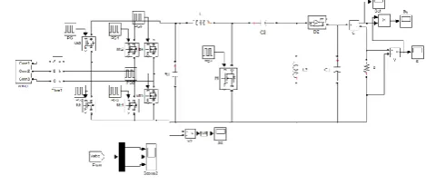
IV.
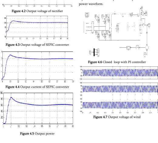
RESULTS AND DISCUSSIONFigure 4 represents the open loop model of SEPIC converter in Simulink. The PWM by applying in the SEPIC converter. The Fig 4.1 a represents the input voltage. Fig 4.2 represents the output voltage of the wind. Fig 4.3 represents the SEPIC Converter output voltage. The Figure 4.4 & Figure 4.5 are represents the inverter produced output current and power waveform
Figrue 4.1 Output voltage of wind
Figure 4.2 Output voltage of rectifier
Figure 4.3 Output voltage of SEPIC converter
Figure 4.4 Output current of SEPIC converter
Figure 4.5 Output power
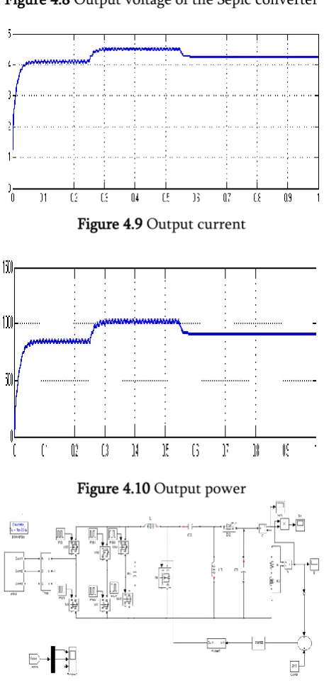
Fig 4.6 represents the PI controller in a closed loop model of SEPIC converter in Simulink. A comparison of the output voltage in DC produced by SEPIC converter were matches the reference voltage. By the application of PI controller there is a reduction in the error. The pulse width is updated by applying PI controller in the SEPIC converter. The Figure 4.7 a represents the input voltage step changes. There is an increment of 4V of input voltage from 50V to 54V. Figure 4.8 represents the SEPIC Converter output voltage. The settled output voltage of 215V was decreased. The Figure 4.9 & Figure 4.10 are represents the inverter produced output current and power waveform.
Figure 4.6 Closed loop with PI controller
Figure 4.8 Output voltage of the Sepic converter
Figure 4.9 Output current
Figure 4.10 Output power
Figure 4.11 Closed loop with FOPID controller
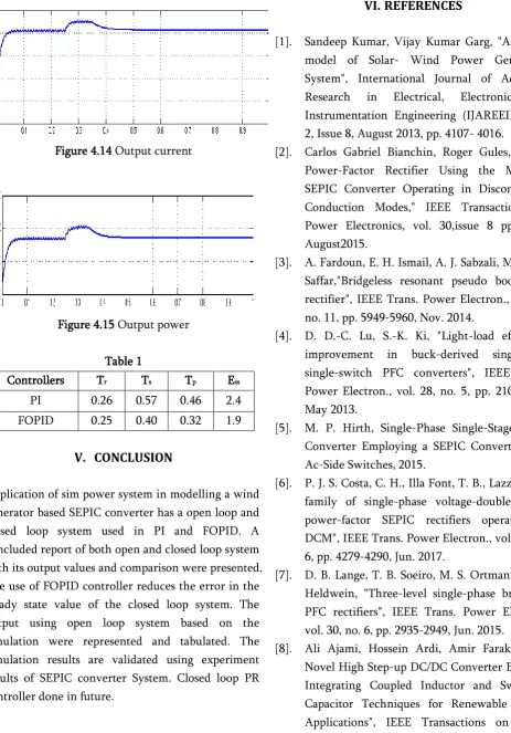
Figure 4.11 represents the FOPID controller in a
comparison of the output voltage in DC produced by SEPIC converter were matches the reference voltage. By the application of FOPID controller there is a reduction in the error. The pulse width is updated by applying FOPID controller in the SEPIC converter. The Figure 4.12 a represents the input voltage step changes. There is an increment of 4V of input voltage from 50V to 54V. Figure 4.13 represents the SEPIC Converter output voltage. The settled output voltage of 215V was decreased. The Figure 4.14 & Figure 4.15 are represents the inverter produced output current and power waveform.
Figure 4.12 Output voltage of wind
Figure 4.14 Output current
Figure 4.15 Output power
Table 1
Controllers Tr Ts Tp Ess
PI 0.26 0.57 0.46 2.4
FOPID 0.25 0.40 0.32 1.9
V.
CONCLUSION
Application of sim power system in modelling a wind generator based SEPIC converter has a open loop and closed loop system used in PI and FOPID. A concluded report of both open and closed loop system with its output values and comparison were presented. The use of FOPID controller reduces the error in the steady state value of the closed loop system. The output using open loop system based on the simulation were represented and tabulated. The simulation results are validated using experiment results of SEPIC converter System. Closed loop PR controller done in future.
VI. REFERENCES
[1]. Sandeep Kumar, Vijay Kumar Garg, "A Hybrid model of Solar- Wind Power Generation System", International Journal of Advanced
Research in Electrical, Electronics and
Instrumentation Engineering (IJAREEIE), Vol. 2, Issue 8, August 2013, pp. 4107- 4016.
[2]. Carlos Gabriel Bianchin, Roger Gules, "High-Power-Factor Rectifier Using the Modified SEPIC Converter Operating in Discontinuous Conduction Modes," IEEE Transactions On Power Electronics, vol. 30,issue 8 pp. 4349, August2015.
[3]. A. Fardoun, E. H. Ismail, A. J. Sabzali, M. A. Al-Saffar,"Bridgeless resonant pseudo boost PFC rectifier", IEEE Trans. Power Electron., vol. 29, no. 11, pp. 5949-5960, Nov. 2014.
[4]. D. D.-C. Lu, S.-K. Ki, "Light-load efficiency improvement in buck-derived single-stage single-switch PFC converters", IEEE Trans. Power Electron., vol. 28, no. 5, pp. 2105-2110, May 2013.
[5]. M. P. Hirth, Single-Phase Single-Stage Ac-dc Converter Employing a SEPIC Converter with Ac-Side Switches, 2015.
[6]. P. J. S. Costa, C. H., Illa Font, T. B., Lazzarin, "A family of single-phase voltage-doubler high-power-factor SEPIC rectifiers operating in DCM", IEEE Trans. Power Electron., vol. 32, no. 6, pp. 4279-4290, Jun. 2017.
[7]. D. B. Lange, T. B. Soeiro, M. S. Ortmann, M. L. Heldwein, "Three-level single-phase bridgeless PFC rectifiers", IEEE Trans. Power Electron., vol. 30, no. 6, pp. 2935-2949, Jun. 2015.
[9]. G. Tibola and I. Barbi, "Isolated Three-Phase High Power Factor Rectifier Based on the SEPIC
Converter Operating in Discontinuous
Conduction Electro technical Conference
(MELECON), 2014 17th IEEE Mediterranean [10]. Y. Zhao, X. Xiang, C. Li, Y. Gu, W. Li, X. He,
"Single-phase high step-up converter with improved multiplier cell suitable for half- bridge-based PV inverter system", IEEE Trans. Power Electron., vol. 29, no. 6, pp. 2807-2816, Jun. 2014.
[11]. S. Saravanan, P. Usha Rani, "Soft Switching