9 | P a g e
DESIGNING FULL ADDER USING n-NOR BASED
THRESHOLD LOGIC GATES
MEKALA B
1, DHEEPIGA M J
2, KRISHNAKUMAR S
3 1,2PG SCHOLAR, DEPARTMENT OF VLSI DESIGN, TKSCT, THENI
3
ASSISTANT PROFESSOR, TKSCT, THENI, TAMILNADU
ABSTRACT
Reduced energy efficiency has always been the major aim of the custom and automated digital circuit design techniques. Although expanding nano-devices are expected to replace the existing MOSFET devices, they are far from being as mature as semiconductor devices and their full potential and promise are many years away from being practical. The research described in this exposition consists of four main parts. It is a new circuit architecture of a differential threshold logic flip- flop called n-NOR. The NNOR gate is an edge-triggered multi-input sequential cell whose next state function is a threshold function of its multi-inputs. a new approach, called hybridization, that replaces flip flops and parts of their logic comes with n-NOR cells is described. The resulting hybrid circuit, which consists of conventional logic cells and n-NORs, is shown to have significantly less power consumption, smaller area, less standby power and less power variation. Another proposed logic is implementation of combinational logic circuits like Half adder and Full adder using the designed n-NOR cell.
Keywords: n-NOR, standard cell, Half adder, Full adder, Threshold Logic Gate
I.
INTRODUCTION
Efforts to reduce power consumption of digital CMOS circuits have been in progress for nearly three decades.
As a result, a number of well understood and proven techniques for reducing dynamic and leakage power have
been incorporated into modern design practices and tools. For instance, some of the ways to reduce dynamic
power include logic synthesis and restructuring to reduce switching activity, gate sizing, technology mapping,
retiming, and voltage scaling, and so on. Similarly, the uses of dual supply and device threshold voltages,
adaptive body biasing, clock and power gating, transistor stacking, and so on are some of the well-known ways
to reduce the power due to leakage. Thus, it appears that the techniques for reducing power at the logic and
circuit levels have been thoroughly explored, leaving little opportunity for improvement. Consequently, the
focus has shifted to the higher levels of design, including power-efficient micro architectures, memory,
compilers, and OS, and system level control, including thermal-aware dynamic frequency and voltage control,
thread migration among processor cores, and so on. One aspect of digital CMOS circuits that has not changed is
how logic functions are computed. A CMOS application-specified integrated circuit (ASIC) using static logic is
a multilevel network of AND/OR logic gates or more complex cells, in which each node computes a Boolean
function of its inputs by establishing a conducting path from the supply rails to its output. However, there exists
10 | P a g e
different mechanisms, which presents the possibility of further improvements in power consumption,performance, and area, which has not been sufficiently explored. As a hard work to reduce power delay of
digital CMOS circuits have been in progress for nearly three decades. As a result, a number of well understood
and proven techniques for low power energy, efficient flip flop design using threshold Logic has been
incorporated into new design software tools. For us, some of the customs to reduce dynamic power include logic
synthesis and restructuring to reduce switching activity, gate sizing, technology Mapping, retiming, voltage
scaling, and so on. Similarly, the uses of dual supply and device threshold voltages, adaptive body biasing, clock
and power gating, transistor stacking, and so on are some of the well-known ways to reduce the power. Thus, it
appears that the techniques for reducing power at the logic and circuit levels have been thoroughly explored,
leaving minor opportunity for improvement power efficiency. Accordingly, the focus has shifted to the highest
levels of design, including power efficient micro-architectures, memory, compilers, and OS, and system level
control, including thermal-aware dynamic frequency and voltage control, thread migration among processor
cores. One part of digital CMOS circuits that has not changed is how logic functions are computed. However,
there exists a proper subset of uniting Boolean functions, called threshold functions, which can be
fundamentally computed by different mechanisms, which presents the possibility of further improvements in
power consumption, performance, and area, which has not been sufficiently explored.
II. THRESHOLD LOGIC GATE
The reason for examining threshold gates as logic primitives stems from the fact that they are computationally
more powerful than the standard AND/OR logic primitives. Many common logic functions, such as the n-bit parity, n-bit multiplication, division, powering, sorting, and so on, can be computed by polynomial size threshold networks of a fixed number of levels, while the same would require exponential size AND/OR
networks. A detailed treatment of the complexity of threshold networks and constructive methods for various
types of arithmetic functions, including size-depth and weight depth tradeoffs. An updated survey of the same
appears in and an extensive survey of circuit architectures of threshold gates is given. These results suggest that
the threshold gates and networks can potentially lead to significant reductions in circuit size and delay. A
threshold function can be implemented in the same way as any logic function, i.e., as a network of logic
primitives or a pull-up network and pull-down network of pFETs and nFETs. Such implementations offer
nothing new, and in fact, can be quite inefficient for implementing large fan-in threshold functions in terms of
speed, power, and area. The implementations of a threshold logic gate (TLG) considered in this paper compute
the predicate in by performing a comparison of some electrical quantity, such as charge, voltage, or current. This
is what distinguishes such implementations of a threshold gate with any of the conventional implementations of
CMOS logic functions. However, the use of TLGs in conventional ASIC design has not been thoroughly
explored due to the lack of efficient and reliable gate implementations and the infrastructure required for
11 | P a g e
III. NNOR TECHNOLOGY
As mentioned earlier, NMOS (nMOSFET) is a type of MOSFET. An NMOS transistor is made up of n-type
source and drain and a p-type substrate. When a voltage is applied to the gate, holes in the body (p-type
substrate) are driven away from the gate. This allows forming an n-type channel between the source and the
drain and a current is carried by electrons from source to the drain through an induced n-type channel. Logic
gates and other digital devices implemented using NMOSs are said to have NMOS logic. There are three modes
of operation in an NMOS called the cut-off, triode, and saturation. NMOS logic is easy to design and
manufacture.
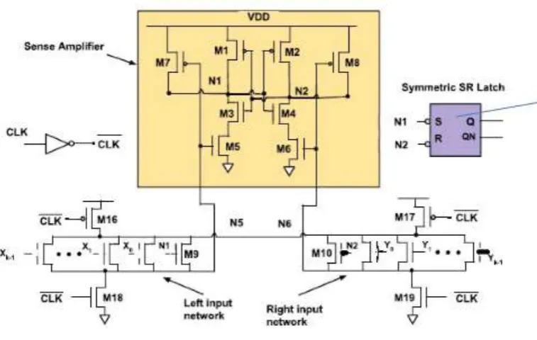
Fig 1. NNOR cell for SR Latch
But circuits with NMOS logic gates dissipate static power when the circuit is idling, since DC current
flows through the logic gate when the output is low. A schematic diagram of the Threshold Logic flip-flop
(TLFF) is presented in the circuit is composed of a semi-dynamic front-end comprising a differential current
switch Threshold Logic gate (DCSTL) followed by a static back-end comprising an SR latch. DCSTL front-end
comprises a fast latched comparator and two parallel-connected sets of unit nMOS transistors, referenced as
input data bank and threshold mapping bank. The nMOS transistors from the threshold mapping bank have the
gates hardwired to ground or power supply With respect to the circuit from the TLFF h 4 data inputs and 4
threshold mapping inputs.
The data inputs, X0, X1, X2, X3 and the threshold mapping inputs, T0, T1, T2, T3 have the weights
12 | P a g e
discharge devicesM18 and M19 pull nodes N5 and N6 low, which turn OFFM5 and M6, disconnecting all pathsfrom N1 and N2 to ground. In addition, M7 and M8 are active, which results inN1 and N2 being pulled high.
The nFETs M3 and M4 are ON. With N1 and N2 being high, the state of the SR latch doesnot change. In this
the weights are implemented using parallel-connected sets of 1,2, 3 and 4 unit transistors respectively. The total
conductance‘s of the transistor banks are compared each other by the latched comparator and therefore the node
X is logic zero if the current generated by the data bank is greater than the current generated by the threshold
mapping bank and logic one otherwise.
Fig 2. NNOR cell for Half Adder
Consider by design, the data bank is prevented from having similar conductance with the threshold
mapping bank, when the threshold is reached, since an nMOS transistor with weight 0.5 is always on. This
prevents the latch comparator entering in a metastable state.
Fig 3. Half adder circuit
The operation of circuit is as follows. On the falling edge of the clock, the flip-flop enters in precharge
phase. Therefore, M10, M11, are on, nodes X and Y are precharged high and the outputs Q and Qbar and hold
their previous evaluation values; since X and Y are high, M6, M7 are on pulling their sources to weak high
13 | P a g e
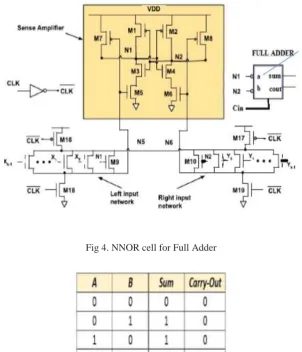
Fig 4. NNOR cell for Full AdderFig 5. NNOR cell for Full Adder
the end of the evaluation phase, the high-rising node among X and Y will be decoupled from being connected to
ground by one of the shutoff transistors M6,M7 going off.
2. For the specific signal assignment used in the technology mapping, the maximum number of active devices
in the LIN or RIN among all the functions process in that realized by an n-NOR.
3. Therefore, the simulation starts with applying a CLK-0 input, which results in N1 = 0, N2 = 1, and Q = 1.
While CLK is held at 1, the input is switched to 0/5, so that N5 = HiZ1.
4. Next, N5 is discharged to ground through a capacitor, which turns OFF M5 and turns ON M7, pulling N1 =1
5. As a result, the conductance of the LIN is higher than that of the RIN.. This corresponds to when CLK 0 → An input that results in ℓ active devices in the LIN and r active devices in the RIN is denoted by ℓ/r. The signal will ensure that ℓ ≠ r. Assume that ℓ > r
IV. SIMULATION RESULTS
The proposed N-nor Threshold logic gates are designed, implemented and was analyzed using Synopsys
14 | P a g e
1. The waveforms from the SPICE simulation of an n-NOR gate extracted from layout, NOR gate withand without transistors M9 and M10. Therefore, M5, M8,9 are on and
Fig 6. Simulation Results of NNOR cell SR latch
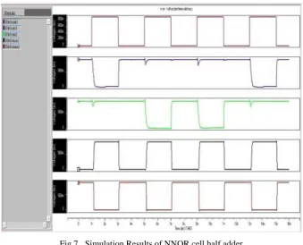
Fig 7. Simulation Results of NNOR cell half adder
As the discharge devices, M18 and M19 are turned OFF, both N5 and N6 will rise to 1. discharge is impeded as
M2 turns ON, resulting in N2 getting pulled back to 1. As a result, the output node N1 is 0 and N2 are 1. As the
15 | P a g e
Fig 8. Simulation Results of NNOR cell full adderIn that current research in the use of threshold logics flip-flops includes new retiming algorithms, the design of
asynchronous circuits, threshold logic-based field-programmable gate arrays, nonvolatile threshold logic
flip-flops, and the combinations conventional logics of these different design approaches.
V. CONCLUSION
In this experimental results shows that the proposed transistor transistor logic gates (TTL), when operated at the
nominal voltage, can be made robust in the presence of process variations. However, dynamic voltage scaling,
which is now an integral part of the power management of most digital circuits, must be limited when applied to
threshold gates due to the presence of the latch-based SA. The degree to which the voltage of a n-NOR cell can
be reduced depends on k—with lower voltages for smaller k. By using the threshold logic gates we have
implemented the half adder, full adder and SR latch operation which all worked well with reduced power
consumption.
REFERENCES
1. Niranjan Kulkarni, Member, IEEE , Jinghua Yang,Member,IEEE , Jae-Sun Seo, Member, 2016.
―Reducing Power, Leakage, and Area of Standard-Cell ASICs Using Threshold Logic Flip-Flops‖ IEEE
transactions on very large scale integration (vlsi) systems.
2. Borivoje Nikolic, G. Vojin Oklobd zija, Vladimir Stojanovic, Wenyan Jia, James Kar-Shing Chiu and
Michael Ming-Tak Leung, 2000. ‗Improved Sense-Amplifier-Based Flip-Flop:Design and Measurements‘,
IEEE Journal of Solid-State Circuits, 35(6): 876-884.
3. Celinski, P., J.F. Lopez, S. Al-Sarawi and D. Abbott, 2001. ‗Low power, high speed, charge recycling
16 | P a g e
4. Hakan Ozdemir, Asim Kepkep, Banu Pamir, Yusuf Leblebici and UgurCilingiroglu, 1996. ‗A CapacitiveThreshold-Logic Gate‘, IEEE Journal of Solid-State Circuits, 31(8): 1141-1150.
5. Hidialgo-Lopez, J.A., J.C. Tejero, J. Fernhdez and A. Gago, 1995. ‗New Types of Digital Comparators‘,
IEEE International Symposium on Circuits and Systems, 1: 29-32.
6. Javier Lopez-Garcia, Jose Fernandez-Ramos and Alfonso Gagobohorquez, 2004. ‗A Balanced Capacitive
Threshold-Logic Gate‘, Analog Integrated Circuits and Signal Processing, 40: 61–69.
7. Jose Quintana, M., J. Maria Avedillo, Raul Jimenez and Esther Rodriguez-Villegas, 2001. ‗Practical
Low-Cost CPL Implementations of Threshold Logic Functions‘, Proceedings of the 11th Great Lakes
symposium on VLSI, New York, pp: 139-144.
8. Koji Kotani, Tadashi Shibata, Makoto Imai and Tadahiro Ohmi, 1998. ‗Clock-Controlled Neuron-MOS
Logic Gates‘, IEEE Transactions on Circuits and Systems-II: Analog and Digital Signal Processing, 45(4):
518-522.
9. Marius Padure, Sorin Cotofana and Stamatis Vassiliadis, 2003. ‗Design And Experimental Results of a
CMOS Flip-Flop Featuring Embedded Threshold Logic‘, Proceedings of the International Symposium on
Circuits and Systems, 5: 253-256.
10. Preeti Ranjan Panda, Aviral Shrivastava, B.V.N. Silpa and Krishnaiah Gummidipudi, 2010.
‗Power-efficient System Design‘, Springer, pp: 1-253.
11. Reto Zimmermann and Wolfgang Fichtner, 1997. ‗Low-Power Logic Styles: CMOS Versus
Pass-Transistor Logic‘, IEEE Journal of Solid-State Circuits, 32(7): 1079-1090.
12. Roland Strandberg and Jiren Yuan, 2000. ‗Single Input Current-Sensing Differential Logic (SCSDL)‘,