LOW POWER DESIGN OF DOUBLE
TAIL COMPARATOR USING SLEEPY
STACK TECHNIQUE
VanshikhaSingh
M.E.Scholar, Departmentof Electronics & Communication Engineering NITTTR,Chandigarh, UT, India
Rajesh Mehra
Associate Professor, Department of Electronics & Communication Engineering NITTTR, Chandigarh, UT, India
Abstract: As the technology evolved from micron to submicron the threat of leakage power dissipation arises which dominates the dissipation of dynamic power. For past several years, technology scaling is the most important procedure for the improvement of the performance of circuit in terms of the power, speed etc. In this paper, design and analysis of double tail comparator with sleepy stack technique is done in terms of power, delay and power delay product.Comparator is the very important circuit in the Analog to Digital converter design. In analog to digital converters, the performance limiting element is the internal gain of the different stages of the amplifiers and the comparator circuits. The accuracy of the comparators which is used in the ADC circuits is defined in terms of power and speed. Several ADCs require small delay, Low power comparators with small die size.So a modified design of double tail comparator is presented with reduced power and delay. It is observed that in the proposed comparator power, delay and pdp is reduced having values of 218.6nwatts, 276ps and 6.048 * 10-17 respectively.
Key Words: ADC, Double-tail Comparator, Dynamic Comparator, Low power design, Power Gating
Technique.
1. Introduction
A comparator is a device that compares two voltages or currents and outputs a digital signal indicating which is larger. Comparator is a circuit that compares one analog signal with another analog signal or a reference voltage and outputs a binary signal based on the comparison and works on two phases: reset and regeneration phase 1. It is a very crucial component of an analog to digital converter (ADC).Analog to digital converter is a device that converts a continuous physical quantity (usually voltage) to a digital number. The conversion involves quantization of input, so it necessarily introduces a small amount of error. It is an iterative method. The inverse operation is performed by a digital to analog converter (DAC).
the comparators produces output of “0.” 4.
Inthe first order circuit design, the calculation of the traditional noise analysis process is depend upon the theory of white sense stationary noise signals.Sinusoidal steady state analysis technique is used for the assumption where every method for system transient are rejected. Such type of analysis technique is applied on several applications of electrical and electronics engineering. There are several techniques which also rely on transient reaction. Renownedmethodsare present for examining the non-random signals in several systems such as convolution; differential equations and Laplace transform methods. Approaches for examininginterferences signals in transient schemes also present but these schemes are not as extensivelyuseful to the first order examination of circuit difficulties5.
In modern world of handy and portable devices like computers, mobile phone, laptops in which power is the major issue in VLSI designs. Power consumption is the topic of great interest. As we know that the batteries provide the limited power to the main device so the circuitry of the main device in such a way that it consume less power. Large power dissipation of the device requires additional circuit which is costly used for noise compensation. Comparators is the most important component in digital design so reducing the consumption of power in comparator circuit is one of the most important issue of low power design. There are many power saving procedures which is involved in the optimization of the sub threshold leakage current due to power supply results the variations in the circuits6.Factors like high speed, full swing output, and consumptionof small power and high value of input impedance, regenerative dynamic latched comparator are widely important circuits for several applications like ADCs, data receivers, zero crossing detector and memory sensing applications7.
Continuous technology scaling is cause of this reduction. For past several years, technology scaling is the most important procedure for the improvement of the performance of circuit in terms of the power; speed etc. because of these scaling’s, supply voltage and threshold voltage is reduced for the MOS transistors in submicron processes. When the reduction in supply voltage occurs, the dynamic power is reduced but static power dissipation is increased due to the leakage current. Transistor dimensions are also a very important parameter to get the optimized performance of the circuit6-7.
2. Regenerative Comparators. 2.1 Conventional Comparator
The conv Decision circuit is because o supply vo terminals different down to applied. W started to when VIN
2.2Conve
In fig. 3, (PMOS a voltage a which pr low offse and secon allows tu transistor VDD and node fn a voltage t decreased
ventional dyn n Making Phas shut down o of transistor M oltage to the t s of the circui discharging r (VDD–Vth) wh When PMOS o charge to V N1is less than V entionalDoub
a convention and NMOS) as compared to rovides the fa et it provide s nd is decision urning on M3 rs MRI and MR
transistors M and fp start to to the back t d rate of kickb
namic compar se.In the time or in off mode M1 and M4. In tail transistor a t, the outn an rate. If VIN1> here Vth is the transistor wil VDD while outp
VIN29. ble Tail Comp nal dual tail co in which cloc o conventiona st latched ope mall current a n making phas and M4 tran R2 is pull down Mtail1 and Mtail2
discharge wi to back invert back noise10.
Fig 2. Schemat
rator perform of reset phase e, and both th n the decision and transistor d outp which
>VIN2, so Outp e output voltag ll turn on, the pdischarge to
parator omparator is p
ck is applied. al comparator eration which and Mtail1. For se.in reset mo nsistor which n the output v 2becomes ON ith a rate if IM ter and deliv
tic of Basic Dyna
ms their opera e the clock app he outputs wh
making phas become on.N is already pre p will discharg ge of the thres latch restorat
ground. The
presented. In d . This compa r. This compar
do not depen r their operatio de, clock is eq pre-charge th voltage to the N. This conditi Mtail/Cfn(p). T vers a worthy
mic Comparator
ation in two plied to the ci hich is outn an
e, we apply th Now when the
e charged with ged sooner th shold voltage ion acquires b circuits perfo
double tail com rator can per rator provides nd upon input on, comparato qual to zero, M he fnand fp no
ground. In de ion causes to The transistor protecting a
important ph ircuit is zero a nd outp achiev he clock signa input voltage h the VDD is g han Outn whic of the transis by back-to-bac orm their ope
mparator circu form their fu s large current t common mo or have two st Mtail1 and Mtai ode to VDD. B ecision making turn off M3 a MR1 and MR2 among input a
hases. Reset P and tail transis ves a certain al which is eq
s is applied to going to disch ch means Ou stor where inp
ck inverters. T eration in reve
uit have two t unction in sma
t to the latch a ode voltage an tages and is re il2 is off. This Because of thi g phase, clock and M4. The v 2 passes the d
and output, c
Phase and storsof the
level VDD qual to the o the input harge with tp to drop put VIN1 is Then, outn erse mode
The trans fp to VD complete certain m point is t through t concern switches phase the in the cha
When we combinat dynamic several p implemen from mic dynamic As we kn and anoth 5, when a avoid the save such
sistor MC1 wh DD so that th ely10.So after manner which to be chosen f transistors M two NMOS t are placed be eir correspond arging path of
e implement a tion of both
power.So if procedures to nt low power cron to subm
power. That’s now that CMO her is pull do a current find e direct conne h power dissip
F
hich is the cont he transistor
some time th results the re for concern th MC1, M1 and M
transistors wh etween the pat ding switch tra
f fp becomes o
any circuit in static and dy we improve decrease the r circuit design
icron the thre s why this tec OS circuit is m own network w the direct pat ection betwee pation. The ga
Fig4 Schematic of
trol transistor MC2 keep in he difference eduction in th hat when trans MTAIL1 which hich works as th of fn and fp ansistor is clo open to save t
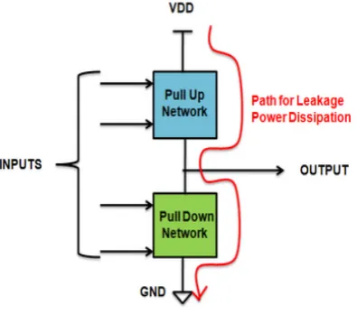
3. Pow
nto hardware, ynamic power
the technolog consumption n. Power gati eat of leakage chnique is very made up of tw which is made th from VDD to en the VDD to ate which is us
f Modified Doub
for the voltag n off position
between volt he time of latc sistor MC1 bec cause the co a switch is i p to the groun osed and let it he static powe
wer Gating Te
power is the r and 50% su gy scaling, th of power. Po ng is used sav e power dissip y much emplo wo network on
e from NMOS o ground, then
ground throu sed to cut dow
le Tail Comparat
ge at node fn b n and the vo
tages at fn an ch generation come on, a cu nsumption of inserted in th d. When fn go
discharge com er reduction.
echnique
major issue f upply of tota he power con ower gating is ve the leakag pation arises oyed in recent ne is pull up n S. The CMOS n the circuit di ugh gate if co wn the direct p tor
becomes on p ltage at node nd fp node i.e . In the opera urrent find a p f static power e circuit i.e M oing to discha mpletely but t
for considerati al power dissi nsumption is
s one of techn e power. As t
which domin time socs. network whic S circuit is sho issipates the le onnection is n path is known
ulls the voltag e fn to be d e ∆Vfn/fp inc ation of this c
ath towards th r. So to overc MSW1 and MS arge in decisio the switch whi
ion. Total pow ipation is pro
decreased11. nique which i the technology nates the dissi
ch is made fro own in Fig 5. eakage power not needed the as power gate
ge at node discharged creases in circuit one he ground come this W2. These on making ich places
wer is the ovided by
There are is used to y evolved ipation of
Fig 5 CMOS Circuit
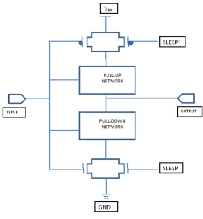
Fig 6 shows the power gating structure. In this fig a low and high threshold voltage transistor are connected to the ground and VDD respectively. These transistors are known as sleep transistors. For power saving operation there are two modes: active mode and sleep mode. In power gating technique a low threshold CMOS circuit is connected to the high threshold module known as sleep transistors. During active operation sleep input is equal to zero and both PMOS and NMOS sleep transistors will become on and because of this we may get a virtual power supply and ground to perform the normal operation. In sleep mode, the NMOS and PMOS sleep transistor is equal to zero because sleep input is equal to one and the direct connection between ground and VDD will broke. Because of this operation the leakage power reduction is reduced in CMOS circuit. But there is a point that because of sleep NMOS and PMOS transistors some extra power is dissipated which is very small compared to the main CMOS circuit consisting pull up and pull down network. The sleep transistors are designed in such a way that they have a high threshold voltage due to which a reduction in excess leakage power occurs in the operation in normal mode 13.
Fig 6 Power Gating Structure
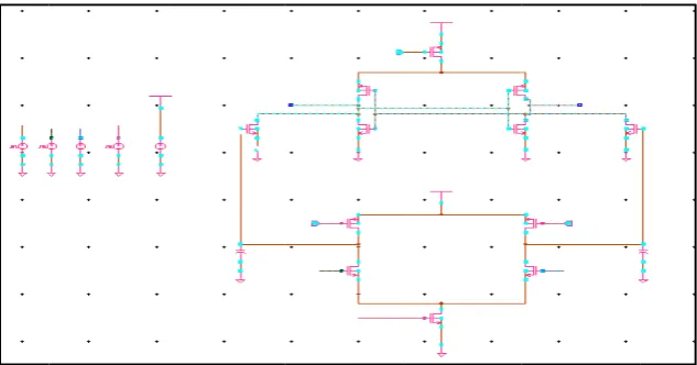
3.1 Proposed Double Tail Comparator
The sche modified transistor of time i current re mode.
As the w power ba accompli
ematic of pro d design trans rs are less than in the active m
educes the sta
world is emer ackup’s devic ished by addin
oposed double sistors Mtail1 n the transisto mode. This p atic power. Th
F
rging with the ces so a majo ng towards the
Fig 7
e tail compar and Mtail2 a ors in which cl rocess reduce he static pow
Fig 8 Schematic o
4.
e several batt or urge drive e small area co
Sleepy Stack Tec
rator using sl are break into lock is applied es the dissipat
er is reduced
of proposed Doub
Result Anal
tery oriented the research onsuming pro
chnique
eepy stack te o two sleep tr d. So the sleep tion of leakag
in sleep mod
ble Tail Comparat
lysis
applications, area towards ocess15-16.
echnique is sh ransistors. Th p transistors a ge current. Re de and the del
tor
there is requ s reduction in
hown in Fig he time period are on for a sh
eduction in th lay is reduced
uirement for t n power which
8. In the d of sleep hort period he leakage d in active
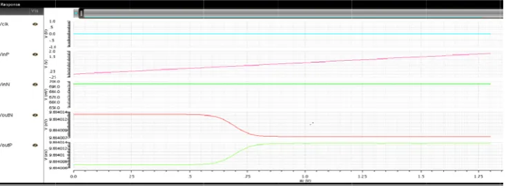
The conv 800mV, of5mV w of circuit Fig.10. It delay of 6
The prop input vol clock pul examined observed 276.7 ps
ventional dua input voltage with clock puls t is examined t is observed f 603 pswith pd
posed dual tail ltage varies fr lse of 600mV d through the d from the ana
with pdp of 6
Fig 9T
al tail compar e varies from
se of 600mV h through the t from the analy dp of 17.125*
l comparator rom 695mV to
having rise ti transient anal alysis that the 6.048 * 10-17.
Transient analysis
rator is obser m 695mV to 7 having rise tim transient analy ysis that the po
10-17.
Fig 10. DC ana
is observed b o 705mV, ref ime and fall ti lysis of 80ns i e power cons
of conventional
rved by simu 705mV, refere
me and fall tim ysis of 80ns i ower consump
alysis of Double T
y simulated in ference voltag
ime of 0.08ns is shown in fi sumption of th
Double Tail Com
ulated in 180n ence voltage me of 0.08ns a s shown in fig ption of this c
Tail Comparator
n 180nm tech ge of 700mV, and time peri ig.11 and the D his comparato
mparator
nm technolog of 700mV, c and time perio g.9 and the D comparator de
hnology with s common mod iod of 1ns.Th DC analysis i or design is 2
gy with suppl common mod od of 1ns.The DC analysis is esign is 28.4*1
supply voltag de voltage of5
e operation of is shown in Fi 218.6 nW and
ly voltage de voltage operation shown in 10 -6Wand
in 180nm voltage o 0.08ns an comparis the bette power de
The auth & Resea provision
m technology of 700mV, com
nd time perio son to the conv
r performanc elay and powe
PAR
TEC
SUPPL
P
D
PDP (PO PR
hors would als arch, Chandiga
nduring this re
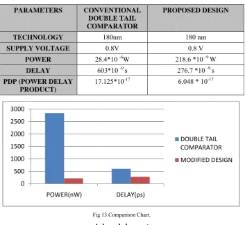
0 500 1000 1500 2000 2500 3000
with supply mmon mode v d of 1ns, it is ventional dou e in terms of er delay produ
RAMETERS
HNOLOGY
LY VOLTAG
POWER
DELAY
OWER DELA RODUCT)
so like to expr arh, India and esearch work.
POWE
voltage 800m voltage of 5m s observed tha uble tail compa f power, delay uct (pdp).
Table 1
CONV DOU COM
GE
28 60
AY 17
Fig
Ac
ress gratitude d H.R.Institut
R(nW)
mV, input vo mV with clock at the power a arator. It is ob y and PDP. I
1. Comparative A
VENTIONAL UBLE TAIL MPARATOR
180nm 0.8V .4*10 -6W 03*10 -9 s
.125*10-17
13.Comparison C
cknowledgem
to Director, N te of Technol
DELAY(p
oltage varies pulse of 600m and delay is r bserved that th In this paper
Analysis
L PRO
2
Chart.
ment
National Instit logy, Ghaziab
ps)
from 705mV mV having ris reduced in du he proposeddu
we present th
OPOSED DES
180 nm 0.8 V 218.6 *10 -9 W
276.7 *10 -9 s 6.048 * 10-17
tute of Techni bad for their e
DOUBLE TA COMPARAT
MODIFIED D
V to 695mV, se time and fa ual tail compar ual tail compa he analysis in
SIGN
W s 7
ical Teachers’ endlessmotiva
IL
TOR
DESIGN
reference all time of rator with arator give n terms of
References
[1] Chandrahash Patel, Dr. Veena C.S., “Study of Comparator and their Architectures,” International Journal of Multidisciplinary Consortium, Vol. 1, pp. 1-12, June 2014.
[2] SarangKazeminia, MortezaMousazadeh, KhayrollahHadidi and AbdollahKhoei, “High-Speed Low-Power Single-Stage Latched-Comparator with Improved Gain and Kickback Noise Rejection”, IEEE Journal of solid-state circuits, Vol.2, pp.216-219, 2010. [3] Swetasahu, Ajay vishwakarma, “Implementation of a low-kickback-noise latched comparator for High-speed analog-to-digital designs
in 0.18µ,” International Journal of Electronics Communication & Instrumentation Engineering Research and Development. Vol. 2, pp. 43-56, december 2012.
[4] Raja Mohd. Noor Hafizi Raja Daud, Mamun Bin IbneReaz, and LabonnahFarzanaRahman, “Design and Analysis of Low Power and High Speed Dynamic Latch Comparator in 0.18 μm CMOS Process”,International Journal of Information and Electronics Engineering, Vol. 2, pp. 944-947, November 2012.
[5] A. Boni and C.Morandi, “High speed, low power BiCMOS Comparator using a pMOS variable load”, IEEE Journal of solid-state circuits. vol. 33,no.1, pp. 143-146, January 1998 .
[6] Anjali Sharma, Rajesh Mehra, “Area and Power Efficient CMOS Adder Design by Hybridizing PTL and GDI Technique”, International Journal of Computer Applications,Volume 66, pp., No.4, March 2013.
[7] TanviSood, Rajesh Mehra, “Design a Low Power Half-Subtractor Using .90μm CMOS Technology”, IOSR Journal of VLSI and Signal Processing, Volume 2, Issue 3, pp. 51-56, May – June 2013.
[8] V.Kowsalya, “Design of A Low Power Double Tail Comparator Using Gated Clock and Power Gating Techniques”, International Journal of Review in Electronics & Communication Engineering, Volume 2, Issue 1, pp.30-33, February 2014.
[9] Wei Wang, Yu-Chi Tsao, Ken Choi, SeongMo Park, Moo-Kyoung Chung, “Pipeline power reduction through single comparator-based clock gating”, International System on chip Design Conference(ISOCC), pp. 480-483, 2012.
[10] SamanehBabayan-Mashhadi and Reza Lotfi, “Analysis and Design of a Low-Voltage Low-Power Double-Tail Comparator” IEEE Transactions On Very Large Scale Integration (VLSI) Systems, Vol. 22, No. 2, pp. 343-352, February 2014.
[11] WeixiangShen, YiciCai, Xianlong Hong, Jiang Hu,“An Effective Gated Clock Tree Design Based on Activity and Register Aware Placement”, IEEE Transactions on Very Large Scale Integration Systems, Volume 18, Issue 12, pp.1639-1648,October 2009. [12] PradeepSingla, KamyaDhingra, Naveen Kr. Malik, “DSTN (Distributed Sleep Transistor Network) for Low Power Programmable
Logic array Design”, International Journal of Computer Applications, Volume 45, No.17, pp. 31-36, May 2012.
[13] B. J. Blalock,“Body-driving as a Low-Voltage Analog Design Technique for CMOS technology,” in Proceedings of IEEE Southwest Symposium, Mixed Signal Design, pp.113–118, Feburary 2000.
[14] B. Goll and H. Zimmermann, “A 0.12 μm CMOScomparator requiring 0.5V at 600MHz and 1.5V at 6 GHz”, in Proceedings of IEEE International Solid-State Circuits Conference, Digest of Technical Papers, pp. 316–317, February 2007.
[15] Nikoozadeh and B. Murmann, “An analysis oflatched comparator offset due to load capacitor mismatch”, IEEE Transactions On
Circuitsand Systems II, Express Briefs, volume 53, No. 12,pp. 1398–1402, December 2006.