Abstract— Superlattice emitter resonant tunneling bipolar transistor (SE-RTBT) is facing problem due to thermal transfer of electrons over barrier which causes diminishing negative differential resistance (NDR) effect. Therefore resonant tunneling diode (RTD) with higher quasi-bound state energy causes transfer of electrons by RT effect instead of thermal process. The RT effect can be enhanced by controlling the barrier and well widths of RTD. It has been found that InP/GaInAs SE-RTBT shows better NDR characteristic at room temperature.
Index Term— S uperlattice emitter resonant tunneling bipolar transistor (S E-RTBT), negative differential resistance (NDR), resonant tunneling diode (RTD), quasi -bound state, Multiple barriers RTD (MBRTD).
I. INTRODUCTION
The Resonant Tunnelling diode (RTD) is a nano -scale quantum diode. Diode is the simplest two terminal active electronic devices. Multiple barriers RTD (MBRTD) show the interesting characteristics of resonant tunnelling for certain quasi-bound energy states. The transmission probability of incident particles can be even one though barriers have a low
transparency. Esaki et al. have done the pioneer work on the
resonant tunneling phenomena [1] and later a large number of theoretical work have been carried out by many research groups [2-4]. The double barrier diode was the primary electronic device whose operating principle depends mainly on the quantum size effect.
M. H. Chowdhury is a graduate student in the Department of Electrical and Computer Engineering, Concordia University, 1455 de Maisonneuve West, QC, H3G 1M8, Canada (corresponding author to
provide phone: 514-848-2424, Ext -7236; e-mail: [email protected]).
M. A. Mannan is a graduate student in the Department ofElectrical and Computer Engineering, Concordia University, 1455 de Maisonneuve
West, QC, H3G 1M8, Canada (corresponding author to provide phone: 514-848-2424, Ext -7236; e-mail: [email protected]).
S. A. Mahmood is a graduate student in the Department ofElectrical and Computer Engineering, Concordia University, 1455 de Maisonneuve West, QC, H3G 1M8, Canada (corresponding author to provide phone:
514-848-2424, Ext -7236; e-mail: [email protected]).
The existence of negative differential resistance (NDR) at room temperature makes RTD as one of the most promising two terminal quantum effect device for applications such as in memory device, oscillator, amplifier in a wide range of frequencies [5, 6]. The tunneling action occurs so rapidly that the effect of transit time is negligible and thus smaller amount of signal distortion occurs [7, 8]. Therefore, high-frequency applications are feasible by using the tunnel diode. RTD shows good performance due to its high speed, large dynamic range of operation, low leakage current but it cannot be controlled like three terminal transistors. It has good application in oscillating circuits and digital switching due to its NDR characteristics. Therefore, RTD is incorporated with normal bipolar transistor (BJT) which is called Resonant Tunneling Bipolar Transistor (RTBT). The concept of RTBT was first proposed by Cappaso and Kiehl [9]. Both the gain and speed of RTBT are improved in comparison with conventional BJT. Resonant-tunneling bipolar transistors (RTBTs) have attracted considerable attention for applications, such as analog-to-digital converters , frequency multiple-valued logic circuits, parity bit generators , high speed switches, oscillators, signal amplifiers etc.
In this paper we will compare the performance of different RTBTs as well as the challenges to prepare RTBT for better desired performance. The effect of both barrier width and well width on the transmission of carriers (electron) through the RTBT has been investigated theoretically.
II. T HEORY
In quantum mechanics wave functions can penetrate through potential barrier. For energies below the top of the barrier the wave is attenuated and it decays exponentially. It takes a significant distance for the decay to eliminate the wave completely. If the barrier is thinner than this critical distance the wave can excite a propagating wave in the region beyond the barrier i.e. tunneling occur.
Room Temperature NDR Performance of GaInAs
based SE-RTBT
V (x)
x
x=0
x=b
I
II
III
Fig. 1. Simple rectangular tunneling barrier.
Let us consider a flux particle of energy E is incident on a
potential barrier of height V0 and width b as shown in Fig. 1. In
the three region of interest the solutions of Schrodinger equations are
1 1
,
)
0
(
jkx jkxI
x
A e
B e
x
1 1
, 0
( )
x xII
x
C e
D e
x
b
1
1
,
jkx jkx
III
x
E e
F e
x
b
Where
2
2
mE
,
2
(
V
O)
E
k
h
h
andA1, B1, C1, D1, E1, F1 are six plane wave co-efficient. By applying
the boundary condition we get the transfer matrix of a single potential barrier as,
1 11 12 1
1 21 22 1
0
(1 )
0
jkb
jkb
A
e
E
B
e
F
where
2 2
11
2
k
Cosh
b
j
Sinh
b
k
,
2 2
21
2
j
k Sinh b
k
, and
22
11 ,* *12 21
.
Since we are interested in the tunneling of a particle from one side to other, we treat an incoming wave from one of the
two sides. So putting F1 = 0 we get A1 = μ11 E1. The
transmission probability is the ratio of the currents on the two sides of the barrier and is given by,
2 11
1
T
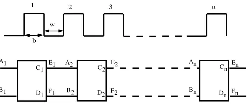
Let us now consider n tunnel barrier width of each is b and they are separated by quantum wells of width w as shown in Fig.2. A1 An Cn En Fn Dn Bn B1 C1 D1 E1 F1 A2 D2 C2 E2 F2 B2 n w b
1 2 3
Fig. 2. T op; n rectangular tunneling barrier, bottom; block diagram of n rectangular barrier.
The overall transfer matrix of n number of tunnel can be expressed as
1 11 12 11 12 1 21 22 21 22
11 12 21 22 1 11 12 1 21 22
0
...
0
0
0
...
0
0
0
0
jkw jkw jkw jkw jkw jkwj nb n w
n
j nb n w n
A
e
B
e
e
e
e
e
E
e
F
e
By multiplication the above equation can be expressed by a single matrix as
11 12
1
21 22
1
(2)
n n n
n n n
E
A
F
B
As there is no incoming wave beyond nth barrier so putting Fn =
0, the overall transmission probability can be expressed as
2 11
1
n nT
III. SE-RTBT
Superlattice is a structure composed of periodically alternating crystalline layers of several materials with different properties (e.g. band gap). In our case sandwich of two different materials with different band gap is used in an alternating periodic order to have the effect of resonant tunnelling (RT) in emitter region of BJT. Fig. 3 shows
AlInAs/GaInAs superlattice as an example. Different
AlInAs GaInAs AlInAs GaInAs AlInAs
Eg
Fig. 3. AlInAs/GaInAs superlattice.
BJTs show good current capabilities over field effect transistor due to their three-dimensional capabilities but they suffer for gain, emitter efficiency and speed. The gain of BJT can be improved by high emitter doping and low base doping. BJT gain is defined by
(
)
nb dte(3)
pe atb
D
N
BJT
D
N
where, doping concentration in emitter, and
dte d
Emitter
N
N
x dx
doping concentration in base,
atb a
Base
N
N x dxBut heavy emitter doping cause emitter band gap shrinkage and low base doping increases the base spreading resistance
which in-turn decrease the unity power gain frequency , fm ax.
To overcome this problem heterojunction concept has been introduced in base-emitter junction. Besides this using RTD in emitter region gives high speed and high gain. The main purpose of using superlattice in emitter region is basically as follows:
1) The superlattice (RTD) is used for hole confinement in base region (Fig. 4) which improves the emitter efficiency of BJT. For npn transistor the emitter efficiency is given by,
(4)
Ene
En Ep
I
I
I
where, IEn=Electron current from emitter to base and IEp=hole
current from base to emitter. If hole is confined in base, IEp is
decreased and emitter efficency is increased and this in-turn increases the current gain.
Electron Tunneling
Hole Confinement
Emitter
Base
Collector
Ec
Ev
Fig. 4. Effect of superlattice in theAlInAs/GaInAs SE-RT BT .
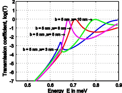
2) The superlattice creates resonant tunneling route for electrons from emitter to base as shown in Fig. 4. Electrons moves at a high speed from emitter to base and so base-emitter transit time decreases which improves the speed of the device and frequency response. Therefore, using RTD in emitter region improves the overall BJT performance. But it is very challenging to select appropreate RTD for emitter region. Both the barrier width and well width controls the transmission of carriers through the RTD. Fig. 5 shows the transmission
coefficient versus energy for InP/ In0.53Ga0.47As double barrier
tunneling system. The barrier width of InP is 5nm and well
width of In0.53Ga0.47As varies from 3nm to 10nm.
Fig. 5. Variation of transmission probability in InP/ In0.53Ga0.47As double tunnel barrier for fixed InP barrier with different In0.53Ga0.47As well.
Fig. 6. Variation of T ransmission probability in InP/ In0.53Ga0.47As double tunnel barrier for different InP barrier.
IV. POT ENT IAL SE-RT BT
In this section we will investigate the performance of different superlattice in emitter region to get the room temperature NDR effect and good current gain along with smaller collector-emitter offset voltage.
A. AlInAs/GaInAs SE-RTBT
In Al0.48In0.52As/Ga0.47In0.53As SE-RTBT Al0.48In0.52As
(Eg=1.22 eV) work as barrier and Ga0.47In0.53As (Eg=0.85eV) work
as quantum well [10], [11]. Here, 20 period Superlattices are
used with 500A0 n-GaInAs emitter region [12]. Al0.48In0.52As/
Ga0.47In0.53As is chosen as resonant tunneling device due its
good material properties as shown in Table- I:
T ABLEI
ALINAS/GAINAS SUP ERLATTICE PROP ERTIES,[12]
Properties AlInAs/GaInAs
S uperlattice Band
discontinuity
∆EV 0.50 eV
∆EC 0.53 eV
Surface recombination velocity
of GaInAs 10 cm s−1
The high valence band discontinuity (∆EV) gives good hole
confinement in base region and increases the emitter efficiency. The low recombination velocity of GaInAs improves
gain. Al0.48In0.52As/ Ga0.47In0.53As superlattice is lattice matched
i.e. strain free structure. Therefore, the mobility of electrons will not degrade and the growth will be easy. This SE-RTBT shows lower turn-on voltage and the collector-emitter offset voltage is about 90mV [12].
In this SE-RTBT, NDR regions are observed only in low temperature. The band diagram is shown in Fig. 7. The
quasi-bound energy is E1=0.123 eV and E2=0.48 eV and width of these
energy bands are 0.004 eV and 0.06 eV respectively [12].
E2 E1
Collector Base
Emitter
EC
EV EF
Fig. 7. Energy Band Diagram of AlInAs/GaInAs SE-RT BT .
The NDR phenomena are observed in the output characteristics of this device at 77K temperature as shown in Fig. 8. Here, the first NDR regions are dominant then the second one. From Fig. 7 it shows that second quasi-bound state is nearer to the top of the barrier so many electrons travel
directly over the superlattice rather than tunnel through the E2
band and so the second NDR is relatively insignificant compare to the first one. On the other hand at higher temperature say in room temperature so many electrons gain enough thermal energy to overcome the barrier directly rather than tunnel through it and so RT action and NDR phenomenon are not observed in the output characteristics . The disadvantages of this device are: (i) low temperature (77k) NDR phenomena is observed but at high temperature (even at room
temperature) it is vanished, (ii) the current gain is very low (
13), (iii) number of superlattice period is high (20).
Fig. 8. Common-emitter output characteristics (Ib=0.1 mA/step) of AlInAs/GaInAs SE-RT BT at 77K. Data are taken from reference, [12].
B. InP/GaInAs SE-RTBT
(1.3μm and 1.5 μm) and this device also has good thermal
conductivity (0.68 w cm-1°C-1) with low turn-on voltage [10].
Again the electron mobility of InP is high. Therefore, it is very suitable for high speed operation. In this SE-RTBT both the
InP and Ga0.47In0.53As is lattice matched so the growth of this
superlattice is strain free and easy to grow. Here InP work as
barrier (Eg=1.34 eV) and Ga0.47In0.53As as quantum well [10].
The properties of this superlattice are shown in Table-II.
T ABLEII
INP/GAINAS SUP ERLATTICE PROP ERTIES [13]
Properties InP/GaInAs
S uperlattice Band
discontinuity
∆EV 0.35 eV
∆EC 0.25 eV
Turn-on voltage 0.34V
Here, the valence band discontinuity (∆EV) is smaller than
the previous structure but it shows good hole confinement in the base region. This device shows smaller conduction band discontinuity then the previous one which results smaller collector-emitter offset voltage of 60mV [13]. Therefore the
power loss is less in this device. Tsai et al. used this device
structure for their SE-RTBT. For their device 5 periods InP
(5nm)/ Ga0.47In0.53As (8nm) is used ins tead of 20 periods. Here,
emitter size is decreased to 100A0. In the previous device
emitter size was five times higher than this. If the emitter thickness is high the transis tor has inferior hole confinement. This causes charge storage in neutral-emitter region which enhances base recombination current as well as total base current. The hole diffusion length of the GaInAs is very low which causes huge decrease in current gain under large base
emitter voltage (Vbe)[13]. By decreasing the emitter length this
problem has been removed. This SE-RTBT shows high current gain of 670 [13].
In InP/GaInAs Superlattice three quasi-bound states has
been observed at E0=0.73 eV, E1=0.95eV and E3=1.18eV [13].
Here the first quasi-bound state energy is almost double than second quasi-bound state energy (0.48 eV) of AlInAs/GaInAs
SE-RTBT. Therefore this device shows good RT
characteristics at high temperature. The NDR phenomena are observed in the output characteristics of this device at room temperature as shown in Fig. 9. Three NDR regions occur even at room temperature which was missing in the previous SE-RTBT. Here, the voltage differences between two NDR regions
are identical (∆∆Vbe∼ 0.22 V) that is the difference of high field
voltage is identical. Therefore, if the superlattice quasi-bound state energy is high with high barrier height, NDR effect can be observed at room temperature.
Fig. 9. Forward base-emitter I-V charact eristic at room temperature. Data are taken from reference [14].
V. CONCLUSION
SE-RTBT shows the controlled NDR characteristic, which is absent in RTD. The NDR effect in SE-RTBT is temperature dependent. At high temperature better thermal transfer of electrons over barrier results in AlInAs/GaInAs SE-RTBT as its quasi-bound state energy is small. This causes diminishing RT phenomena. InP/GaInAs SE-RTBT shows better NDR performance even at room temperature. The higher quasi-bound state energy of InP/GaInAs SE-RTBT prevents thermal transfer of electrons over barrier. Thus nano-scale resonant tunnelling diode with conventional BJTs shows the controlled NDR region and improves the current gain of BJTs.
REFERENCES
[1] R. T sui, and L. Esaki, “ T unneling in a Superlattice,” Applied Physics Letters, vol. 22, pp. 562-564, Jun. 1973.
[2] H. Yamamoto, “ Resonant T unneling Condition and T ransmission Coefficient in a Symmetrical one-Dimensional Rectangular Double Brarrier System,” Applied Physics . A, vol. 42, pp. 245-248, Oct. 1986.
[3] B. Ricco, and Ma.Ya.Azbel, “ Physics of Resonant T unneling. T he One Dimensional Double-barrier Case,” Physical Review. B, vol. 29, no. 4, pp. 1970-1981, Feb. 1984.
[4] E.E. Mendez, E. Calleja, and W. I. Wang, “ T unneling T hrough Indirect -gap semiconduct or barriers,” Physical Review. B, vol. 34, no. 8, pp. 6026-6029, Oct . 1986.
[5] M. T suchiya, H. Sakaki, and J. Yoshino , “ Room T emperature Observation of Differential Negative Resistance in AlAs/GaAs/AlAs Resonant T unneling diode,” Journal of Applied Physics, vol. 24, pp. L466, 1985.
[6] T .C.L.G. Sollner, P.E. T annenwald, W.D. Goodhue, and D.D.Peck, “ Quantum Well Oscillators,” Applied Physics Letters,
vol. 45, no. 12, pp. 1319-1321, Aug. 1984.
[7] T .C.L.G. Sollner, W.D. Goodhue, P.E. T annenwald, C.D. Parker, and D.D. Peck, “ Resonant tunneling T hrough Quantum Wells at frequencies up to 2.5 T Hz,” Applied Physics Letters, vol. 43, no. 6, pp. 588-590, Jul. 1983.
[9] F. Capasso, and R. A. Kiehl, “ Resonant tunneling transistor with quantum well base and high-energy injection: a new negative differential resistance device,” Journal of Applied Physics, vol. 58, pp. 1366-1368, Aug. 1985.
[10] Ioffe Physico-T echnical Institute. http://www.ioffe.rssi.ru/SVA/NSM/ as of July, 08, 2010.
[11] U. K. Mishra, J. Singh, “ Semiconductor Device Physics and Design,” 1st ed., T he Netherlands, Springer, ISBN 978-1-4020-6480-7, P.-539, 2008.
[12] Shiou-Ying Cheng, Wen-Lung Chang, Wen-Chau Liu “Investigation of an AlInAs/GaInAs super lattice-emitter resonant tunneling bipolar transistor (SE-RT BT ),” Superlattices and Microstructures, vol. 22, no. 4, 1997.
[13] Jung-Hui T sai, King-Poul Zhu, “ Investigation of InP/InGaAs superlattice-emitter resonant tunneling bipolar transistor at room temperature,” Solid-State Electronics, vol.47, pp.1055–1059, 2003.
[14] Jung-Hui T sai, Yu-Chi Kang, I-Hsuan Hsu, T zu-Yen Wen “Investigation of InP/InGaAs super lattice-emitter bipolar transistor with multiple negative-differential-resistance regions,”

![TABLE INP /GAINAS SUPERLATTICE II PROPERTIES [13]](https://thumb-us.123doks.com/thumbv2/123dok_us/1395314.1651114/5.612.337.553.56.234/table-inp-gainas-superlattice-ii-properties.webp)
