e-ISSN: 2278-7461, p-ISSN: 2319-6491
Volume 6, Issue 3 (March. 2016) PP: 22-27
Design of a low power 12bit SAR ADC with self calibration
Wang Jun
1, Zuo Yan
21
School of Electronics and Information Engineering, Tianjin Polytechnic University, Tianjin ,China
2School of Electronics and Information Engineering, Tianjin Polytechnic University, Tianjin ,China
Abstract: This paper introduces a low power 12bit SAR ADC for portable EEG sensor .The influence on accuracy capacitance error and parasitic capacitance is discussed in detail. An self-calibration circuit is designed on the traditional structure,it greatly reduces the effect of capacitance error and improve the
conversion accuracy of ADC。The design adopts CMOS 0.13 m process,the simulation results show that
when the input signal bandwidth is 50Hz and the clock frequency is 7.8kHz with adding the calibration circuit,
SNDR reached 71.47dB, and ENOR reached 11.51bit,and INL value decreased from 6LSB to 0.25LSB.The
circuit adopts 1.2V power supply, power consumption is about 26W, which can meet the requirements of application of portable sensors.
Keywords: EEG; SAR ADC; DAC; self-calibration
I.
INTRODUCTION
EEG (Electroencephalogram) monitoring is an important means for clinical diagnosis and disease prevention-control. In order to make a more comprehensive and accurate judgment of the human health, we need to monitor the EEG for a long time, and collect and analyze the information continuously. But the traditional EEG medical monitoring equipment can not continue for too much long time, so the research and application of EEG portable monitoring equipment gradually has become a hot topic.ADC (Analog to digital converter) is an important part of portable EEG sensors which can transform analog signals into the digital signals who can be applied to machine recognition. Portable sensors ADC need to work for a long time, therefore it is necessary to design the circuit with low power consumption. At the same time the circuit processing signal frequency is low, the high speed is not necessity. SAR ADC (Successive Approximation Register Analog-to-digital Conventer) has the characteristics of medium speed, medium precision and low power consumption which can meet the above requirements.Due to the current process conditions, SAR ADC is difficult to achieve requirements of the 12bit resolution, where the split capacitor charge redistribution DAC is affected by capacitor mismatch and parasitic capacitance. Therefore DAC circuit need to join the calibration technology to improve the resolution of ADC. Literature[1] adds adjustable capacitance to compensate the nonlinear error. But the chip area occupied by this structure is directly proportional to the precision after calibration, so it requires a great sacrifice of the chip area to achieve better accuracy, where is not suitable for portable devices. In literature [7], 11bit SAR ADC makes use of DAC self capacitance array self calibration by digital logic control instead of joining additional calibration circuits, which greatly reduce the chip area occupied. But by this method, the effective bits of calibration circuit can only reach 9.93bit, which is far lower than the resolution of the circuit requirements. In this paper, an adjustable capacitor circuit with the style of binary weighted capacitor array is connected between the low side capacitor array and the ground for calibration. Simulation results show that this design improves the ADC resolution and greatly reduces the chip area occupied by calibration circuit.
II.
THE
DESIGN
OF
SAR
ADC
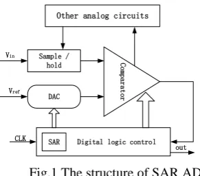
2.1SARADC PRINCIPLE
Other analog circuits
Sample / hold
DAC
C
omp
ara
t
or
Digital logic control SAR
Vin
Vref
CLK
out
Fig.1 The structure of SAR ADC
2.2DAC DESIGN WITH SELF CALIBRATION
According to the requirement of low power consumption of portable EEG sensor, in this paper, the DAC is designed by using binary segmented capacitor charge redistribution DAC structure. The structure of the the DAC circuit is mainly composed of capacitors, so this structure consumes less power than other ones[4]. As shown in Fig.2 (a), the traditional 12bit split capacitor charge redistribution DAC structure consists of a split capacitorCsand a both-sides capacitor array. Its working principle is as follow:
When all the capacitors are connected Vin and the upper plate is grounded, DAC enters the sampling phase.
At this point, the charge of node P is:
p= - 6 4 * i n
Q C V (1)
Then the bottom plate of the capacitor is grounded and upper plate break with ground, where the output voltage of DAC Vp is equal to Vin. Then switch S1 2 connects Vr e f , which lead the circle into redistribution phase of the
charge. At this time the voltage of point P :
p in re f
1
= - +
2
V V V (2)
If Vpis larger than 0, it means that
1
2 f
in re
V V , where the comparator output is high level; if Vpis smaller than 0,
the comparator output is low level. Then Vinwill respectively compare with 1 4 r e f
V , 3
4 r e f
V ,and so on, until the
end of the compare between last bit in the logical control and Vin.
Vref
Vin
C C 2C 4C 8C 32C C 2C 4C 8C 16C 32C
X P
gnd
S0 S1 S2 S3 S4 S5 S6 S7 S8 S9 S10 S11 S12 Sc
16C
Cs=64 63C
Vref Vin
C C 2C 4C 8C 32C CP1 C 2C 4C 8C 16C 32C
CP2
X P
CP3
gnd
S0 S1 S2 S3 S4 S5 S6 S7 S8 S9 S10 S11 S12
Sc 16C
Cs= 64 63C
Cc
Left Right
(a) The traditional 12bit split CDAC circuit (b)A 12bit split CDAC circuit with calibration
Fig. 2 The circuit of 12bit CDAC
Since the capacitance value of the split capacitor is not an integral multiple of the unit capacitance, DAC will introduce a capacitance error value Cp2. At the same time, on the left and right sides of the capacitor array on the plate will also generate the node capacitance Cp1and Cp3. The three error capacitances greatly reduce the conversion accuracy and linearity of the DAC, therefore, in this paper, an self calibration method is proposed to eliminate the error caused by the above problems. As shown in Fig. 2 (b), the part of capacitance Ccis self
calibration circuit. When the Ccdo not be considered, the error caused by Cp1, Cp2andCp3 mainly occurred in the sampling stage. So switch of S0~S12 connect Vinand switch of Sc is grounded. The voltage of point X is the
partial pressure of Vinat X:
1 2
6 4
6 4
x in
p s p
C
V V
C C C C
Calculate equivalent capacitance the left of P:
2 _
1 2
( ) 6 4
6 4
s P e q L
P s P
C C C
C
C C C C
(4) At this time, the high 6 bit capacitor on the right side of P connect Vin, and parasitic capacitanceCp3 is grounded at both ends. Therefore, the total charge of P in sampling stage for savings:
_ _
_
( ) 6 3 ( )
( 6 3 )
p s a m p le e q L in in e q L in
Q C V C V
C C V
(5)
By formula (4), formula (5), because of the influence of Cp1,Cp2 that he equivalent capacitance on the left of P deviate from the unit capacitance when sampling, there will be sampling error. If Ce q_L=C , the sampling error can be eliminated where the total charge of P can achieve 6 4C V in.
In the X point access to a adjustable Cc, it is parallel with the Cp1.Assumption P look left equivalent
capacitance is Ce q_L1, then the Ce q_L1 expression is as follows:
2
_ 1
1 2
( ) 6 4
6 4
s P e q L
P c s P
C C C
C
C C C C C
(6)
Make Ce q_L1 equal to the unit capacitance, the value of the calibration capacitor can be obtained from the formula (6):
2 1
k
2 1 2 1
6 3 ( ) 6 4
6 3 2 -1 , 8
c s P P
P P P P
C C C C C C
C C C C k
(7)
where k is the number of capacitors on the left. The sampling error can be eliminated from the formula (7) , but the calibration capacitor also has an effect on charge redistribution. First of all, the sampling phase ends up in the hold phase. When S0~S12 is grounded, the Sc is disconnected, then the equivalent capacitance on the left of P is as follow:
2
_ q 1 2
6 3
( 6 4 ) // ( )
6 4
P
e q P c s P
C
C CC C C C C (8)
The voltage of P:
_ h o ld
2 3 6 4 6 3 6 4 6 4 p in P P C V V C C C (9)
In charge redistribution phase, the potential of P is the sum of partial pressures of Vp_h o l d and Vr e f :
2 3 k 2 3 k 2 3 6 4 6 3 6 4 6 4
6 4 1
6 3 2
6 4
6 4
6 4 1
( )
6 3 2
6 4
6 4
P i n
P P
r e f P
P
i n r e f P P C V V C C C C V C C C C V V C C C (10)
Drawn from the above calculation, the calibration capacitor can be completely eliminated in nonlinear circuit distortion, but when the sampling stage is completed, a capacitance error is introduced in the left of P, which has the value of 6 3Cp2 / 6 4. Finally, a factor of less than 1 is introduced when the comparator input
voltage Vpis generated. Increasing the gain of the comparator can counteract this factor, which has little effect on the normal operation of the ADC.The logic control part of the calibration circuit is shown in Fig.3, where Cc is a binary weighted form of calibration capacitance. The calibration process of DAC is as follows:
Connect S0~S6 toVr e f , and S7 is connected to the ground with the switch Sc is closure. Charging for P, then the
charge of p:
_
( )
P c m e e q L r e f
Then switch S0~S6 is connected to the ground, and switch Sc is off with the switch S7 connected to Vr e f . The
output voltage of p:
q _ 1 q _ 1
q _ 1
q _ 1
q _ 1 q _ 1
( )
c m e L e L r e f P
e L r e f e L
c m r e f
e L e L
V C C C V
V
C C
C V C C
V V
C C C C
(12)
By comparing the value of Vp and Vc min the comparator, the result of the comparator output to the logic control part, then adjust the value of Cc, until the two voltages is equal.
Vref Vin
C C 2C 4C 8C 32C CP1 C
CP2
CP3
Gnd
S0 S1 S2 S3 S4 S5 S6 S7 16C
Cs= 64 63C
Logic control section
P
Vcom Sc Cc
S1
S2 S3 S4 S5 C
C C C
C C C 2C 4C
A
The Circuit of calibration capacitor Cc
Fig.3 The circuit of DAC calibration
The formula (7) shows that the value of adjustable capacitorCcfor calibration consists entirely of parasitic
capacitanceCp1and split capacitor error Cp2, relative to the effect on the error of the expanded 2k-1 times. Without calibration, it is very difficult to control the equivalent capacitance of the segmented capacitor and the capacitance array of the left side by the traditional layout design.
III.
SIMULATION
RESULTS
At the current technology, Cp1 is generally not greater than 1C, and Cp2is not greater than 0.1C. Here it
assumes worst case where Cp1is 1C andCp2 is 0.1C. The figure of INL (Integral Non-linearity, integral
nonlinear error) by MATLAB is shown in Fig.4.
(a)The INL value without calibration (b)The INL value of the calibration circuit with step length of 0.25C
(c)The INL value of the calibration circuit with step (d)The INL value of the calibration circuit with step
length of 0.5C length of 1C
Fig. 4 The change of INL value caused by the step size of the calibration circuit
been less than ±0.5LSB. At this time, the performance has meet the requirements of circuit design. But this value is easily affected by external environment.So the circuit selects the step size of the 0.25C, and the INL value is ±0.22LSB.The calibration circuit of step length is designed to 0.25C, which is the trade off between the number of unit capacitors and the resolution requirements.The simulation of ADC using Spectre simulation tool in Cadence software, input signal is sine wave with the frequency of 30Hz, and frequency of sampling circuit is 7.8kHz. Sampling points of the simulation results of Cadence is 4096, the frequency spectrum of data by MATLAB is as shown in Fig.5.
Fig. 5 The output spectrum of SAR ADC after calibration
Fig.5 shows that the SNDR reaches 71.47dB with the circuit utilizing calibration, and the effective bits reach 11.51bit. From Table.1, compared with paper [1], this paper not only increases the resolution of ADC, while reducing the power consumption of the circuit. When it comes to paper [7], the ENDR and INL value in this paper are closer to the design precision, and calibration circuit is stronger to eliminate the nonlinear error.
Table.1 Simulation and comparison
Paper[1] Paper[7] This work
Technology 65nm 0.13m 0.13m
Supply voltage 1.2V 0.5V 1.2V
Resolution 8bit 11bit 12bit
Power consumption 1.83mW 730nW 26W
SNDR 45.7dB 5.5dB 71.47dB
ENDR 7.3bit 9.93bit 11.51bit
INL -0.3/+0.3LSB -1.47/+1.83LSB -0.25/+0.25LSB
IV.
CONCLUDING
This paper introduces the design of a self calibration with split capacitor charge redistribution DAC 12bit SAR ADC by technology of CMOS 0.13μm. The self calibration method based on split charge divided type DAC circuit is added in the form of binary weighted adjustable capacitor array, which eliminates the parasitic electric capacity and nonlinear error caused by capacitor mismatch effectively. The effective number of ADC reached 11.51bit, and the INL value is controlled within -0.25~+0.25LSB, the overall power consumption is only 26μW. Compared with other paper, this work achieves higher precision and lower power consumption.
V.
ACKNOWLEDGEMENTS
Tianjin application foundation and advanced technology research program (021286).
REFERENCES
[1] Chen Y, Zhu X, Tamura H, et al. Split capacitor DAC mismatch calibration in successive approximation ADC[C]// Custom Integrated Circuits Conference, 2009. CICC '09. IEEE. IEEE, 2009:279-282.
[2] Wu C, Yuan J. A 7 bit 800MS/S SAR ADC with background offset calibration[C]// IEEE International Symposium on Circuits and Systems. IEEE, 2016.
[3] Chen C, Wang B. An ultra low power 10-bit 1KS SAR-ADC for ECG signal recording applications[C]// China Semiconductor Technology International Conference. 2016.
[4] Rahman M, Chen L, Sun N. Algorithm and implementation of digital calibration of fast converging Radix-3 SAR ADC[J]. Proceedings IEEE International Symposium on Circuits and Systems, 2014. [5] Khan M A, Kerkhoff H G. Studying DAC capacitor-array degradation in charge-redistribution SAR
[6] Cai J, Mei-Hua X U, Ran F. Design of a 10Bit successive approximation A/D converter[J]. Semiconductor Technology, 2004, 29(4):73-76.
[7] Um J Y, Kim Y J, Song E W, et al. A Digital-Domain Calibration of Split-Capacitor DAC for a Differential SAR ADC Without Additional Analog Circuits[J]. Circuits & Systems I Regular Papers IEEE Transactions on, 2013, 60(11):2845-2856.
[8] Yoshioka M, Ishikawa K, Takayama T, et al. A 10-b 50-MS/s 820-W SAR ADC With On-Chip Digital Calibration.[J]. IEEE Transactions on Biomedical Circuits & Systems, 2010, 4(6):384-385.
[9] Hester R K, Bright W J. Charge-redistribution analog-to-digital converter with reduced comparator-hysteresis effects: US, US5675340[P]. 1997.
[10] Liu Y H, Ming-Hua H E. A Design of Digital-to-Analog Converter Based on 14-bit Successive Approximation Analog-to-Digital Converter[J]. China Integrated Circuit, 2010.
[11] Brenna S, Bonetti A, Bonfanti A, et al. A tool for the assisted design of charge redistribution SAR ADCs[J]. 2015:1265-1268.
[12] Brenna S, Bonetti A, Bonfanti A. A simulation and modeling environment for the analysis and design of charge redistribution DACs used in SAR ADCs[C]// Uksim International Conference on Computer Modelling and Simulation. 2014:74-79.
[13] Huang L, Jiang Y, Jiaxin J U, et al. A 12 bit CMOS Fully Differential SAR ADC[J]. Electronics World, 2014.
[14] Chao I J, Huang C C, Wu Y C, et al. A 12-bit 4-kHz incremental ADC with loading-free extended counting technique[M]. 2013.