Prakash et al. World Journal of Engineering Research and Technology
A REVIEW OF LOW POWER FLASH ADC USING THRESHOLD
INVERTER QUANTIZATION TECHNIQUE
Shailendra Prakash*1 and Dr. Vishal Ramola2
1
M.Tech Scholar, Dept. of VLSI Design, F.O.T. Uttarakhand Technical University, Dehradun.
2
Astt. Prof. (H.O.D.), Dept. of VLSI Design, F.O.T. Uttarakhand Technical University, Dehradun.
Article Received on 01/03/2017 Article Received on 22/03/2017 Article Accepted on 11/04/2017
ABSTRACT
Digital signal processing algorithms were becoming increasingly more powerful while advances in integrated circuit technology provided compact, efficient implementation of these algorithms in silicon. In the design of mixed-signal and system on chip (SOC) applications the analog-to-digital converter (ADC), is a key functional block which limits the performance and the speed of the system. The analog-to-digital converter is one of the most important component of signal processing and communication systems. An Analog to digital converter is a circuit that converts an analog signal such as a sound picked up by a microphone or light entering a digital camera, into digital signal. There are different types
of ADCs depending on type of applications. There are three main categories of ADCs depending on the speed of operation i.e. low speed serial ADC, medium speed ADC and high speed ADC. The different types of ADCs based on various topologies are: Flash ADC, Sigma delta ADC, Ramp counter ADC, Successive approximation ADC. The flash ADC is known
for having the fastest speed compared to other ADC architectures. Therefore, it is used for high-speed and very large bandwidth applications such as radar processing, digital oscilloscopes, high-density disk drives, and so on. This paper presents review of Low Power Flash ADC using Threshold inverter quantization technique.
World Journal of Engineering Research and Technology
WJERT
www.wjert.org
SJIF Impact Factor: 4.326*Corresponding Author Shailendra Prakash
M.Tech Scholar, Dept. of
VLSI Design, F.O.T.
Uttarakhand Technical
KEYWORDS: Analog-to-digital converter, Flash ADC, Threshold Inverter Quantization, Comparator, Resolution, Low Power, Encoder.
INTRODUCTION
Naturally occurring signals are analog in nature which are at least at a macroscopic level i.e. these signals are continuous and can take infinity of values. As we know in digital domain the operation and functionality of signals become more accurate and faster than the analog domain. So there must be a circuit needed that converts the naturally analog signals into digital this circuit is known as Analog to Digital Converter. An Analog to Digital circuit converts continuous amplitude and continuous time signals into discrete amplitude and discrete time signals. Digital to Analog Converter is required whenever analog signal is needed back.
FLASH ADC
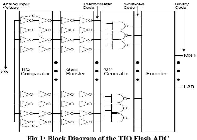
Among various known high speed ADC architectures two most common implementations are the Flash type and the Pipeline architecture. The Flash ADC is faster of two but limited to lower resolution due to a large no. of components (2n-1 comparators for n-bit ADC). The Pipeline ADC architecture is slower of two but is more suitable for higher resolution (require n-stages for n-bit ADC). The Flash ADC is the Fastest ADC among all the ADC architectures available because of its parallel comparator array that facilitates parallel data conversion. A Flash ADC comprises of comprises of two blocks: comparator and encoder. Comparator
block compares the input signal with the reference signal and generate thermocode and the Encoder block converts the thermocodes into digital outputs.
LITERATURE REVIEW
This paper describes low power Flash ADC using Threshold inverter quantization technique with different resolution, supply voltage, and different CMOS technologies.
[01]. “Design of Low Power 0.8v Flash ADC using TIQ in 90nm Technology” Ranam
Sireesha and Abhishek Kumar; introduced a 04-bit low power Flash analog-to-digital converter using Threshold inverter quantization (TIQ) comparator that is this circuit does not require resister ladder that leads to area and power saving. This design operated at 800mv, input frequency of 1KHZ with reduced power consumption of 14.08 µw and 200usec delay. The main purpose of this architecture (i.e. TIQ comparator and a low power high efficient encoder) is to reduce power. This design is simulated using cadence spectre 90nm technology.
[02]. “Design of a TIQ Comparator For High Speed And Low Power 04-Bit Flash ADC”
Sujeet Mishra and Balchand Nagar; define that the major building block for improvement of power and speed specification is comparator. They introduces a new design for comparator with Threshold Inverter Quantization for Flash ADC, that requires 2n-1 comparators for generation of thermocode. The proposed design provides high speed, low power, and smaller area with different P-mos and N-mos widths and power supply of 0.99v. The design is simulated using Tanner tool 0.25um CMOS technology.
[03]. “A Novel Approach to 03-bit Flash ADC” Kalpana Chaudhary and R.B. Singh; proposed that use the digital inverters as analog voltage comparators. This eliminates the requirement of high gain differential input voltage comparators that are inherently more compound and slower than digital inverters. This 03-bit Flash ADC is implemented on 90nm process technology in standard CMOS digital design and simulations are done using Tanner EDA tool with supply 0.9v. This design is highly suitable for the complete SOC integration using the standard CMOS digital process.
[04]. “A 4 GS/s, 1.8v multiplexer encoder based Flash ADC using TIQ technique” Liyaqat
The complete ADC consumes less than 145uw with speed 4GS/s. The proposed TIQ flash ADC has been designed with standard CMOS technology parameters keeping length of channel equal to 0.12µm with 1.8v supply. The simulation is done using HSPICE model (BSIM3).
[05]. “Design method and automation of comparator generation for flash A/D converter”
Daegyu Lee, Jinchoeol yoo, Kyusum Choi; present the design methods and the automation of the comparator circuit layout generation for Flash ADC. The TIQ based ADC require 2n-1 comparator each are different from all others. The authors present an optimal design method of the CMOS TIQ comparators and their automatic layout generation that significantly improves the linearity of the ADC against the CMOS process variation can be almost eliminated. The resulting Flash ADC features higher speed, lower power consumption, smaller size and more readiness for the SOC integration.
[06]. “A 1-GSPS CMOS Flash A/D Converter for System-on-Chip Applications” Jinchoeol
yoo, Kyusum Choi, Ali Tangel; introduce an ultrafast CMOS ADC design that uses TIQ technique for comparator. TIQ is used for high speed. In this paper authors designed a 6-bit TIQ based Flash ADC with 0.25µm standard CMOS technology parameter and it operates with sampling rate upto 1GSPS and power dissipation is 66.87mw at 2.5v and occupies 0.13mm2 area. The proposed ADC is suitable for system-on-chip in wireless products and other ultra high speed applications. Here the device designed with 63 comparators and 63
gain boosters and an encoder.
[07]. “Low-power self reconfigurable multiplexer based decoder for Adaptive resolution Flash ADCs” Chetan Vudadha, Goutham Makkena, M Venkata Swamy Nayudu, Sai
Phaneendra P, Syed Eeshad Ahmed, Sreehari Veeramachaneni, N Mooorthy Muthukrishnan, M.B. Srinivass; present a new improved 2:1 multiplexer based decoder for flash ADCs. The proposed decoder can be configured to operate on thermometer code with reduced length
[08]. “Design of a 1.5v, 4-bit Flash ADC using 90nm Technology” Arunkumar. P. Chavan,
Rekha,G.P. Narashimaraja; introduce a 4-bit analog to digital converter is designed for low power CMOS, which requires 2n-1 comparators, an encoder to convert thermometer code to binary code. This circuit uses a preamplifier and a latch stage. The preamplifier stage to achieve an acceptable gain, and the latch stage consists of two inverters which are connected in a back to back fashion forming a differential comparator and an nmos transistor is connected between the differential nodes of the latch. The circuit operates with an input frequency of 25 MHZ and 1.5v supply with a conversion time of 6.182ns. The design is simulated using cadence environment with 90nm technology, which shows a low power dissipation of 1.984mw for the designed ADC.
[09]. “Simulation and Analysis of 2:1 Multiplexer Circuits at 90nm Technology” Ila Gupta,
Neha Arora, Prof. B.P. Singh; describe that a multiplexer is a unidirectional device that used in application in which data must be switched from multiple sources to a destination. This paper represents the simulation of different 2*1 multiplexer configurations and their comparative analysis on different parameters such as power supply, voltage, operating frequency, temperature, load capacitance and area efficiency etc. All the simulation have been carried out on BSIM 3V3 90nm technology at Tanner EDA tool. Now a days low power
become important consideration as performance and area. This paper consists literature review of different 2*1 multiplexer circuits as; NMOS multiplexer circuit, CMOS multiplexer circuit, Multiplexer single with level restoration (MSL) multiplexer circuit, Multiplexer double (MD) multiplexer circuit, Differential cascade voltage switch logic (DCVSL) multiplexer circuit, Modified differential cascade voltage switch logic (MDCVSL) multiplexer circuit. This paper concluded with the efficient approach of multiplexer. NMOS circuit is showing better result over operating frequency up to the range 200MHZ. MDCVSL circuit shows the least power delay product over a range of supply voltages.
[10]. “Study and implementation of comparator in CMOS 50nm technology” Dharmendra B. Mavani, Arun B. Nandurbarkar; describe the comparator circuits used in Flash ADC. In this paper TIQ and Two stage open loop comparator design styles are described. Two stage open loop comparator is implemented in 50nm CMOS technology. Pre-simulation of comparator is done in LT-Spice and post layout simulation is done in microwind 3.1. Comparator is the “Heart” of the ADC. The inverter threshold is defined as the Vin=Vout in the VTC of an
propagation delay. The two stage open loop comparator has two differential inputs. The advantage of this circuit is that the circuit consumes minimal number of transistors and thus the circuit area is small. Two stage open loop comparator is presented using 50nm CMOS technology.
[11]. “Design of 3-bit low power flash type ADC” Sarojini Mandal, Dr. J.K. Das; define that Simple two stage op-amp with miller capacitance can be used as a high gain comparator. It is simulated in 180nm technology using Cadance Virtuso analog design environment simulation. The op-amp uses a 1.8v Vdd and a 1.8v Vss and consumes power of around
0.9mw. The analog output of each comparator is encoded using cascading full adder designed by transistor logic that makes the circuit more faster. This paper introduces a low power op-amp modified from the traditional one and an encoder employing cascaded full adders with pass transistor logic gates. A current mirror is used as a biasing circuit that is free from voltage sources and utilize current as a reference source. A miller compensation capacitor is used to maintain the stability of the circuit and increase phase margin.
[12]. “Study of a 3-bit CMOS flash ADC utilizing Threshold Inverter Quantization technique” Kalpana Chaudhary, R.B. Singh; describe a 3-bit ADC which is most essential
part of a system-on-chip device as it minimizes the gap between analog and digital world. The proposed ADC utilizes TIQ technique that uses two cascaded CMOS inverters as a comparator. The TIQ technique proposed here for better implementation in SOC applications
using Flash ADC. With the advancement in technology, digital signal processing has gained significant importance in the field of telecommunication, biomedical, control system and so on. Flash ADC is high speed and low resolution device, its high speed is due to of its parallel architecture, all conversions are done in one cycle with many comparators. The name of TIQ
technique is based on the logic of using two cascading inverters as voltage comparators. By using these technique there is no need of voltage comparator and no need of resistor ladder circuit used in conventional Flash ADC. The implementation is carried out on Tanner EDA tool 90nm process technology. The TIQ Flash ADC provides higher data sampling rate and operates at low voltage and also low power consumption.
The TIQ comparator consists of two cascaded CMOS inverters. The analog input signal quantization level is set in the first stage by changing the VTC by means of transistor sizing. The second inverter stage is used for increased gain and logic level inversion so that the circuit behaves as an internally set comparator circuit. The key point about second stage is that it must be exactly same as the first stage to maintain the same DC threshold levels and to keep the linearity in balance for the voltage rising and falling intervals of high frequency input signals.
[14]. “Employing threshold inverter quantization (TIQ) technique in designing 9-bit folding
and interpolation CMOS analog-to-digital converters (ADC)” Oktay Aytar and Ali Tangel; This paper present designing and interpolation of a 9-bit folding and interpolation ADC using 0.35 µm CMOS C35B4 model under AMS-HIT kit library. The complete system consist of two main blocks, one of them is 4-bit flash ADC using TIQ technique and second one is the 5-bit fine ADC part of the converter. The designed converter works with 5v power supply and has analog input range of 34 VPP. Analog input bandwidth is 1MHZ with clock frequency
of 2GHZ for the digital part. The linearity measures of the converter include 2.9LSB of DNL and 6.3 LSB of INL. The main purpose of this paper work is to investigate the possibility o f employing TIQ technique in designing folding and interpolation types ADCs. Although the
linearity measures are not satisfying for 9-bit case. The reduction of comparator count is obtained by analogue pre-processing circuits. The designed converter was also fabricated through Europractice.
[15]. “A Power Efficient 6-Bit TIQ ADC Designed for Portable Applications” Satya Narayan
Mishra, Wasim Arif, Jishan megedi, Srimanta Baishya; present a power efficient ADC is an important module for long lifespan of battery for the portable applications. The high speed
used to increase speed by reducing fan-out in critical path of decoder. The designed ADC works on only 1.23mw of power acceptable linearity error.
CONCLUSION
A simple and fast A/D converter architecture that uses inverter comparator for Flash A/D conversion, named TIQ technique, has been proposed. The TIQ based ADC circuits offer higher data conversion rates while maintain a comparable power consumption level. This paper gives information about the Flash ADC using TIQ technique defined by different researchers with different parameters.
REFERENCES
1. Prof. S.S. Khot, Dr. P. W. Wani, Dr M S Sutaone, Shubhang Tripathi “Design of a 45nm TIQ Comparator for High Speed and Low Power 4-Bit Flash ADC”, 2010.
2. Arunkumar. P. Chavan, Rekha. G, P. Narashimaraja “Design of a 1.5-V, 4-bit Flash ADC using 90nm Technology”, International Journal of Engineering and Advanced
Technology (IJEAT), December 2012; 2(2): ISSN: 2249 – 8958.
3. Liyaqat Nazir, Roohie Naaz Mir, Najeeb-ud-din Hakim “A 4 GS/s,1.8 V Multiplexer encoder based Flash ADC using TIQ Technique.” International Conference on Signal
Processing and Integrated Networks, 2014.
4. Neha Prabhat, Amana Yadav “A Review of Low Power Flash ADC Using Different Comparator Styles and Design Techniques”.ISSN (Online): 2320-9801ISSN (Print): 2320-9798 International Journal of Innovative Research in Computer and Communication Engineering.
5. Ila Gupta1, Neha Arora, Prof. B.P. Singh “Simulation and Analysis of 2:1 Multiplexer Circuits at 90nm Technology” International Journal of Modern Engineering Research (IJMER), 1(2): 642-646. ISSN: 2249-6645.
6. Oktay Aytar and Ali Tangel “Employing threshold inverter quantization (TIQ) technique in designing 9-Bit folding and interpolation CMOS analog-to-digital converters (ADC)”. Scientific Research and Essays, 18 January, 2011; 6(2): 351-362, DOI: 10.5897/SRE10.793 ISSN 1992-2248 ©2011.
7. Sujeet Mishra and Balchand Nagar “DESIGN of a TIQ COMPARATOR for HIGH SPEED and LOW POWER 4 BIT FLASH ADC” Electronics and Communication
8. Sujeet Mishra and Balchand Nagar “ Design of a TIQ Comparator for High Speed and Low Power 4 bit Flash ADC” International Journal of Emerging Technologies in Computational and Applied Sciences (IJETCAS).
9. Kalpana Chaudhary, R. B. Singh “Study of a 3-bit CMOS flash ADC utilizing Threshold Inverter Quantization technique”.IJSRD - International Journal for Scientific Research
and Development, 2(03): 2014.
10.A Variable Threshold Voltage CMOS Comparator for Flash Analog to Digital Converter International Journal of Computer Applications, February 2014; 88(7): 0975–8887. 11.Daegyu Lee, Jincheol Yoo, and Kyusun Choi “Design Method and Automation of
Comparator Generationfor Flash A/D Converter” Department of Computer Science and
Engineering,The Pennsylvania State University, University Park, PA 16802.
12.P. T. F. Kwok and H. C. Luong. “Power Optimization for Pipeline Analog-to-Digital Converter”. IEEE Transactions on Circuits and System II, May 2001; 46(5): 549-553.
13.B. Black. “Analog-to-Digital Converter Architectures and Choices for System Design”. Analog Dialogue, 1999; 33-8.
14.M. Choe, B. Song, and K. Bacrania. “An 8-b 100 MSample/s CMOS Pipelined Folding ADC”. IEEE Journal of Solid-State Circuits, February 2001; 36(2): 184-194.
15.Channakka Lakkannavar, Shrikanth K. Shirakol, Kalmeshwar N. Hosur, “Design, Implementation and Analysis of Flash Adcarchitecture with Differential Amplifier as Comparator using Custom Design Approach” International Journal of Electronics Signals
and Systems (IJESS), 2012; 1(3): ISSN: 2231- 5969.
16.T. P. E. Broekaert, B. Brar, J. P. A. van der Wagt, A. C. Seabaugh, F. J. Morris, T. S. Moise, E. A. Beam III, and G. A. Frazier. “A Monolithic 4-Bit 2-Gsps Resonant Tunneling Analog-to-Digital Converter”. IEEE Journal of Solid-State Circuits, September 1998; 33(9): 1342-1349.
17.D. Dalton, G. J. Spalding, H. Reyhani, T. Murphy, K. Deevy, M. Walsh, and P. Gri_n. “A 200-MSPS 6-bit Flash ADC in 0.6-_m CMOS”. IEEE Transactions on Circuits and
System II, November 1998; 45(11): 1433-1444.
18.“Design of novel high speed dynamic comparator with low power Dissipation For High Speed ADCs” a thesis submitted by Prasun Bhattacharya, NIT, Rourkela, May 2011.
20.C. J. B. Fayomi, G.W. Roberts, and M. Sawan. “A 1-V 10-bit Rail-to-Rail Successive Approximation Analog-to-Digital Converter in Standard 0.18 _m CMOS Technology”. In IEEE International Symposium on Circuits and Systems, 2001; 1: 460-463.
21.The Institute of Electrical and Electronics Engineers, Inc. (IEEE). IEEE Standard for “Teminology and Test Methods for Analog-to-Digital Converters”, IEEE Std, 2001;
1241-2000.
22.6-BIT CMOS FLASH ADC USING TIQ COMPARATOR IN 0.250μM TECHNOLOGY
International Journal of Electronics, Communication andInstrumentation Engineering Research and Development (IJECIERD) ISSN(P): 2249-684X; ISSN(E): 2249-7951, Jun 2015; 5(3): 27-36. © TJPRC Pvt. Ltd.
23.Channakka Lakkannavar, Shrikanth K. Shirakol, Kalmeshwar N. Hosur, “Design,
Implementation and Analysis of Flash Adcarchitecture with Differential Amplifier as Comparator using Custom Design Approach” International Journal of Electronics Signals and Systems (IJESS), 2012; 1(3). ISSN: 2231- 5969.
24.Kalpana Chaudhary, R. B. Singh “Novel Approach to 3-Bit Flash ADC” IJSRD - International Journal for Scientific Research and Development, 2014; 2(03). ISSN (online): 2321-0613.
25.Chetan Vudadha, Goutham Makkena, M Venkata Swamy Nayudu, Sai Phaneendra P, Syed Ershad Ahmed,Sreehari Veeramachaneni, N Moorthy Muthukrishnan, M.B. Srinivas “Low-Power Self Reconfigurable Multiplexer Based Decoder for Adaptive Resolution Flash ADCs” 2012 25th International Conference on VLSI Design.
26.Sagar Mukherjee, Dipankar Saha, Posiba Mostafa, Sayan Chatterjee, C. K. Sarkar, "A 4-bit Asynchronous Binary Search ADC for Low Power, High Speed Applications, International Symposium on Electronic System Design, 2012.
27.“Design of Analog CMOS integrated circuits by Behzad Razavi, Tata Mcgraw hill, 1st Edition, 2002.
28.Pradeep Kumar, Amit Kolhe, “Design and Implementation of LowPower 3-bit Flash ADC in 0.18μm CMOS,” International Journal of Soft Computing and Engineering
(IJSCE), November 2011; 1(5). ISSN: 2231-2307.
BIOGRAPHY
Shailendra Prakash completed his B.Tech degree in Electronics and
Communication Engineering from Dehradun Institute of
Technology, Dehradun (Uttarakhand Technical university, Dehradun) in 2014 and persuading M.Tech scholar degree in VLSI Design from Faculty of Technology, Uttarakhand Technical University, Dehradun. His current research interests include low power VLSI design, Nanoscale and CMOS devices.