The Thickness Effect Of Cuo Thin Films On
Structural, Morphological And Optical
Properties
Sameer Atta Maki & Ons Ahmed Mahmoud
Collage of education for pure science Ibn Al-Haitham university of Baghdad, Baghdad, Iraq.
Corresponding author, E-mail: [email protected]
Abstract—In this studies the Copper Oxide
(CuO) thin films which have been prepared by thermal oxidation with different thicknesses (100,150,200) nm on glass and Si substrates, we made (p-CuO/n-Si) heterojunction was deposited by high vacuum thermal evaporation, These films was tested by X-Ray diffraction and the results confirm of CuO thin films have polycrystalline structure and demonstrate with a preferred orientation (111) (𝟏𝟏𝟏̅)plane, We can study Morphology properties From AFM analysis demonstrate that average. Diameter (grain size) increase with increasing thickness,
The (uv-vis) spectrophotometer discover the direct allowed band gap ,and the energy band gap of CuO thin films were found to be in the range of (2.1eV to 2.4eV) when the thickness of films varying from(100nm to 200nm), and the optical constants calculated such as (absorption coefficient ,refractive index, and extinction coefficient)for wavelength in range (300-1100)nm.
Keywords—CuO, XRD, AFM, UV_VIS, Thermal Oxidation, Morphology properties.
1-Introduction:
The features of Copper Oxide (CuO) thin film is considered to be a p-type semiconductors which have low band gap (1.3-2.1) ev with monoclinic crystal structure [1], the conduction in p-type semiconductors increase by doping or annealing [9], low cost production processing [1,3,5], non-toxic nature [1,3,5],.good electrical and .high optical absorption[5], In additional Copper Oxides effective to Synthesizing PN junction diodes[6], therefore this films of (CuO) suitable in many application such as photovoltaic devices [7] (solar cell, photodetector, humidity and gas sensor [3,6])
and photo-thermal [1], catalytic applications [3], There are several methods of deposition techniques used to prepare copper oxide films such as thermal evaporation [1,3], electrochemical deposition [3], chemical vapor deposition [1,4], sol-gel [1,4], pulsed laser deposition [1,3,4], spray pyrolysis [1,4], plasma evaporation[1], molecular beam epitaxy [1,3], anodic oxidation [7], and reactive RF magnetron sputtering[4]. In this studies we used the thermal evaporation technique to prepare Cu thin film and then we oxidation these films to obtain (CuO) films.
The aim of this study was Focused on the preparing this films to be using in fabricating the heterodiode[10].
2-Experimental:
Firstly We recorded the films thickness by using weighing method [7],Secondly cut slides of glass and Silicon (n-type) with area (2 ×
Edward coating unit model(E306) with molybdenum boat, distance between the substrate and boat was about(9cm), Fifthly, placed these films of Cu in oven type (Kilns Furnaces) to exposing thermal Oxidation processes at (523K) for one hour with exist air at rate flow(1.5) liter/sec, and then the structure properties of these films was examined by X-Ray diffraction method using Shimadzu X-X-Ray diffractometer system 6000, this system records the intensity as function of Bragg angle with operation condition(Source: Cu Kα radiation, wavelength λ:1.5406𝐴°, current = 20 mA, voltage = 4Kv, scanning speed = 5 cm/min).
From Bragg ҆s law we can get information about the crystal structure such as phase crystalline, Crystal size (𝐷), lattice parameter (a), and the inter planer distance d(hkl)for different planes[1].
2𝑑𝑠𝑖𝑛𝜃 = 𝑛𝜆 (1)
n = the reflection order.
𝑎 = 𝑑(ℎ2+ 𝑘2+ 𝑙2)1/2 (2)
The films Crystalline size (𝐷) could be calculated from diffraction line broadening using the Scherrer equation[1].
𝐷 = 0.9𝜆 𝛽𝑐𝑜𝑠𝜃
(3)
β = the full width at half maxima, θ = the angle diffraction, λ = the wavelength of X-Ray.
We can evaluate the strain (ɳ) and the dislocation density (δ) by using the relations [2].
ɳ =𝛽 cos 𝜃 4
(4)
𝛿 = 1 𝐷2
(5)
From (UV-Visible 1800 spectrophotometer) we can measurement optical transmission (T) and absorbance(A) spectrum in the range (300-1100) nm, then we get the band gap (Eg), reflectance (R) and optical constants {absorption coefficient (α), refractive index (n), extinction coefficient (K) } of the deposition films[1].
𝛼 = 2.303𝐴 𝑡
(6)
𝐾 =𝛼𝜆 4𝜋
(7)
𝑛 =1 + √𝑅 1 − √𝑅
(8)
𝑅 = 1 − 𝑇 − 𝐴 (9)
The incident photon energy(hv) was calculated as a function of wavelength(nm) from this equation:
𝐸𝑔 = ℎ𝜈 = ℎ𝑐 𝜆𝑛𝑚
(10)
Where ℎ ∶ is Plank ҆s constant (6.62*10−34J. sec), 𝑐 ∶ is speed of light (3*108)m/sec and 𝜆 ∶ is the Wavelength[8].
𝐸𝑔𝑜𝑝𝑡 = 1240 𝜆𝑛𝑚
(11)
From Tauc formulas which describe the energy depend of absorption coefficient(α) near the band edge for band to band and excitation transition.
(𝛼ℎ𝑣) = 𝐵(ℎ𝑣 − 𝐸𝑔𝑜𝑝𝑡)𝑟 (12)
Where B is a constant inversely proportional to amorphousity,
r is constant indicates to the type of optical
transition and take value (1 2 ,23) for direct
3-Results And Discussion:
(3-1)XRD Analysis:
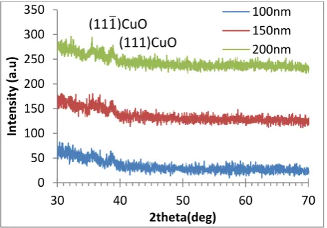
The major tool that which used to knowledge the phases of prepared CuO films is XRD. the pattern in figure (1) for thin film at thickness
(100)nm show two peaks at
(2θ=35.7°,38.7°)with d(hkl) (2.51A°,2.32A°) correspond to orientation (111̅)(111)planes respectively this phase indicates to (CuO), for the films at (150)nm noted two peaks at (2θ=35.5°,38.7°) with d(hkl) (2.52A°,2.32A°) correspond to orientation (11־1),(111) planes respectively, for the film at thick ness (200)nm show two peaks (2θ=35.4,38.7) with d(hkl) (2.52A°,2.31A°) correspond to orientation (111̅)(111) planes respectively with compared the standards (ASTM-card file )No:048-1548 the result of XRD pattern showed that prepared films as different thickness have polycrystalline in nature and monoclinic structure .
Figure (1)XRD pattern of CuO thin films at thickness (100-150-200)nm.
Table 1: XRD analysis results of structural (CuO)thin film with thickness (100)nm.
2θ (deg)
FWHM (deg)
d(A) (hkl) I(a.u)
38.7248 0.7 2.32339 (111) 99
35.7073 0.5 2.5125 (111̅) 100
Table 2: XRD analysis results of structural (CuO) thin film with thickness (150)nm.
θ 2 (deg)
FWHM (deg)
d(A) (hkl) I(a.u)
38.7398 0.57 2.32252 (111) 99
35.514 0.5133 2.52573 (111̅) 100
Table 3: XRD analysis results of structural (CuO) thin film with thickness (200)nm.
θ 2 (deg)
FWHM (deg)
d(A) (hkl) I(a.u)
38.7947 0.68 2.31936 (111) 99
35.4974 0.72 2.52688 )111̅) 100
Table 4: X-Ray Characterization for CuO thin films with thickness(100-150-200)nm.
Thickness (nm)
Avg. Crystalline Size(D)nm
Avg. δ× 1014 lines.m-2
Avg. ɳ
× 10−4 Lines-2. m-4 100 14.28923 53.02288 24.90511 150 15.43498 42.26082 22.99987 200 11.92577 70.54817 29.08729
(3-2)AFM Analysis:
From Atomic force Microscopy (AFM) we can Knowledge the morphology properties for surface ,roughness and grain size[8], the estimated values of root mean square (Sq) ,surface roughness average(Sa) and Average grain size are listed in table (4) We notes with increasing thickness increase Average diameter(Grain size).
0 50 100 150 200 250 300 350
30 40 50 60 70
In
tens
ity
(a
.u
)
2theta(deg)
100nm 150nm 200nm (111̅)CuO
Table5: AFM analysis results of structural of (CuO) thin films with thickness(100-150-200)nm.
thickness(nm) Avg. G.S(nm)
Sa(nm) Sq(nm)
100 78.32 0.848 1.01
150 98.76 0.393 0.464
200 119.87 1.08 1.26
(3-3)UV-VIS Analysis:
From (UV-VIS) spectrophotometer for these film we can conclusion that the optical energy gap found to be in range (2.1eV to 2.4 eV).
Figure.(3)Transmission spectra for CuO thin films with thickness(100-150-200)nm respectively.
Figure(4)Reflectance spectra for CuO thin films with thickness (100-150-200)nm respectively.
0 10 20 30 40 50 60 70 80 90 100
400 600 800 1000
tra
ns
mis
sion
wavelenght (nm)
T-100nm T-150nm T-200nm
0 0.1 0.2 0.3 0.4 0.5 0.6
400 600 800 1000
Reflacta
nc
e
(R)
wavelenght (nm)
R-100nm
R-150nm
R-200nm
Figure.2 -a AFM Image of CuO films at thickness 100nm.
Figure.2 -b AFM Image of CuO films at thickness 150nm
Figure (5) Refractive Index for CuO thin films with thickness (100-150-200)nm respectively.
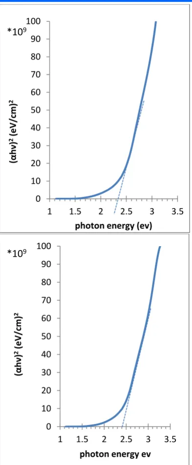
Figure .(6) (αhν)2 versus photon energy gap of CuO thin films with thickness(100-150-200)nm respectively.
Conclusion:
In our research we studied the structure, Morphology and optical properties of CuO thin films as prepared thermal Oxidation by using thermal evaporation in high vacuum , the XRD measurements showed that the CuO thin films have polycrystalline in nature with monoclinic crystal structure, we can calculated the average crystalline size from XRD data is found to 1
2 3 4 5 6 7
400 600 800 1000
Reflective
Id
ex
(n)
wavelenght (nm)
n-100
n-150
n-200
0 10 20 30 40 50 60 70 80 90 100
1 1.5 2 2.5 3 3.5
(
α
h
ν)
2 (eV/cm)
2
photon energy( eV)
*109
0 10 20 30 40 50 60 70 80 90 100
1 1.5 2 2.5 3 3.5
(α
h
ν)
2 (eV/c
m)
2
photon energy (ev)
*109
0 10 20 30 40 50 60 70 80 90 100
1 1.5 2 2.5 3 3.5
(α
h
ν)
2 (eV/c
m)
2
photon energy ev
be(14.2892, 15.4348, 11.257)nm of thickness(100-150-200)nm respectively, we concluded that the Grain Size increase with increasing thickness from (AFM)data , the optical energy gap was Investigated from (UV_VIS)spectroscopy of these films were found to be in the range of (2.1eV to 2.4 eV) when the film thickness varying from(100nm to 200nm ).
References :
1- Bushra K.H.al-Maiyaly, I.H.Khudayer ,Ayser.J. Ibraheim (Effect ambient oxidation on structural and optical properties of copper oxide thin films)International journal of Innovative research in science ,Engineering and Technology ,vol.3 (2014)(8694-8700).
2-Sameer Atta Makki , Hiba M.Ali (Fabrication and characterization of (P-CuO/N-Si) heterojunction for Solar Cell Applications)Journal of Multidisciplinary Engineering Science and Technology ,vol.3(2016)(5053-5055).
3-Amar hadee Jareeze( Optical properties, structure and Morphology of CuO Grown by thermal Oxidation of Cu thin film on Glass Substrate), Journal of Kufa - Physics, Vol.6,No.1(2014)(36-41).
4-RiyamA.Hammoodi, Dr. Ahmed K.Abbas, Dr. Abdullhussein K.Elttayef (Structural and optical properties of CuO thin films prepared via R.F magnetron sputtering) vol.3(2014)(1-7).
5-Hiroki Kidowaki, Takeo Oku, Tsuyoshi Akiyama, Atsushi Suzuki, Balachandran Jeyadevan and Jhon Cuya(Fabrication and Characterization of CuO-based Solar Cells ) vol.1,No.1( 2012)(138-143).
6-V.Saravanakannan&T.Radhakrishnan(
Structural ,Electrical and Optical Characterization of CuO thin films prepared
by spray pyrolysis technique),International Journal of ChemTech Research vol.6,No.1(2014) pp(306-310).
7-Khalid Haneen Abass, Qunoot Mohammed Hadi, Shahad Luay Hamdan, Muneba Mohammed ALagha(Effect of annealing temperature on some optical properties of CuO thin film),Vol.10( 2015).
8- Dr.Afnan K.Yousif, Ban A.Bader,Rana O.Mahdi (Morphological and Optical properties of CuO/Sapphire thin films prepared by pulsed laser deposition), Vol.32,No.5(2014)(892-898).
9-Mohd Rafie Johan, Mohd Shahadan Mohd, Nor Liza Hawari ,Hee Ay Ching (Annealing effects on the properties of copper oxide thin films prepared by chemical deposition),International Journal of Electrochemical Science, Sci.,6(2011) (6094-6104).
10-Aseel M. Abdul Majeed, Ahmed N.Abd, Ali A.Hussen,Nadir F. Habubi (Fabrication and Characterization of copper Oxie Nanoparticales/Psi