STRUCTURAL AND PHYSICAL PROPERTIES OF TORSIONAL CARBON
NANOTUBE DEVICES BY ELECTRON DIFFRACTION AND MICROSCOPY
Taoran Cui
A dissertation submitted to the faculty of the University of North Carolina at Chapel Hill in
partial fulfillment of the requirements for the degree of Doctor of Philosophy in the
Department of Physics and Astronomy.
Chapel Hill
2013
Approved by:
Sean Washburn
Lu-Chang Qin
Jianping Lu
Charles Evans
Adam Hall
ABSTRACT
TAORAN CUI: Structural and Physical Properties of Torsional Carbon Nanotube Devices by Electron Diffraction and Microscopy
(Under the direction of Sean Washburn and Lu-Chang Qin)
This dissertation first probes into the detailed development process of a nanoelectromechanical system based on one-dimensional carbon nanotubes. Various types of carbon nanotubes with a sparse spatial distribution are grown with corresponding chemical vapor deposition recipes. The synthesis is followed by the microelectronic fabrication to pattern a circuit with a suspended carbon nanotube, which allowed thein situ
observation and manipulation of this nano-electromechanical system in a transmission electron microscope. The theoretical deduction and the experimental result prove the sophistication ofin situnanobeam electron diffraction with transmission electron microscopy to determine the chiral structure of a carbon nanotube, especially each individual inner shell of a multiwalled carbon nanotube, while the electron transport behavior of the carbon nanotube is measured. Based on the experimental results of large numbers of carbon nanotubes, a model is established to correlate the transport property with the atomic structure of a carbon nanotube. Given the unambiguous chirality and therefore the explicit band structure, it is concluded that both the thermal excitation and the multiple conducting subbands significantly contribute to the ballistic transport in a carbon nanotube at room temperature.
ACKNOWLEDGMENTS
There are lots of people I would like to thank for a huge variety of reasons.
Firstly, I would like to thank my advisors, Prof. Sean Washburn and Prof. Lu-Chang Qin, without whose common-sense, knowledge and perceptiveness I would have never finished, I can’t overstate the importance of their involvements in my graduate career. I thank both of them for their enthusiasms, kindnesses and encouragements which always supported me, and their timely comments and profound experiences were invaluable throughout.
I am particularly indebted to Dr. Letian Lin, former group member who introduced me into the project and with whom I spent most of my time during PhD, for his patient guidance and precious suggestions, as well as his profound knowledge of ancient Chinese literature for amusements during the tedious late night experiments.
I am grateful to all my colleagues, Dr. Lamar Mair, Dr. Haijing Wang, Dr. Zheng Ren, Nadira Williams, Robert Zhang, and Jerome Carpenter. I will always miss the enlightening discussions with you and the generous help you provided. I would like to express my appreciation to Prof. Jie Tang for the internship opportunity at NIMS and the heart-warming hospitality. I also want to acknowledge Yingwen Chen from Dr. Jie Liu’s group at Duke University for the help in nanotube growth and catalyst synthesis. My sincere regards go to all CHANL personnel, especially Dr. Amar Kumbhar, for the fabrication apparatus support and maintenance.
I owe a debt of gratitude to all my committee members, especially Prof. Jianping Lu, without whose fundamental theoretical work and detailed explanations, all my project would have been unrealistic; and Prof. Adam Hall, thank you for the help and suggestions in experiment design, and your PhD dissertation has been the Bible to me throughout the project.
TABLE OF CONTENTS
LIST OF TABLES . . . x
LIST OF FIGURES . . . xi
LIST OF ABBREVIATIONS . . . xiv
1 Introduction to Carbon Nanotubes . . . 1
1.1 History . . . 1
1.2 From Graphene to Carbon Nanotube . . . 2
1.3 Structure of Single-Walled Carbon Nanotubes . . . 3
1.4 Energy Dispersion of Single-Walled Carbon Nanotubes . . . 6
1.5 Multi-Walled Carbon Nanotubes . . . 9
1.6 Mechanical Properties of Carbon Nanotubes . . . 12
BIBLIOGRAPHY . . . 14
2 Characterization of Carbon Nanotubes . . . 16
2.1 Scanning Tunneling Microscopy and Other Techniques . . . 16
2.2 Transmission Electron Microscopy and Nano-Beam Electron Diffraction . . . 17
2.2.1 Mechanism of Transmission Electron Microscopy . . . 18
2.2.2 Imaging of Carbon Nanotubes in the Real Space with TEM . . . 20
2.2.3 Theory of Electron Diffraction of Carbon Nanotubes . . . 20
2.2.4 Determination of Chiral Structure of a Carbon Nanotube . . . 25
BIBLIOGRAPHY . . . 33
3 Synthesis of Carbon Nanotubes . . . 35
3.1 Introduction. . . 35
3.2 Fundamentals of Chemical Vapor Deposition(CVD) . . . 35
3.2.2 Temperature . . . 38
3.2.3 Catalytic Nanoparticles . . . 38
3.2.4 Gas Flow Rates . . . 40
3.3 CNT Synthesis Experiment . . . 40
3.3.1 Motivation and Objective . . . 40
3.3.2 Experimental Process . . . 42
3.3.3 Synthesis Results . . . 45
BIBLIOGRAPHY . . . 48
4 Nano-Electromechanical Device Based on a Suspended CNT . . . 50
4.1 Introduction. . . 50
4.2 Device Fabrication . . . 51
4.2.1 Basic Configuration . . . 51
4.2.2 Back Etching . . . 54
4.2.3 Fabrication of Circuit and Paddle . . . 54
4.2.4 Suspending Nanotube . . . 58
4.3 Customized NEMS Specimen Holder forin situTEM . . . 61
BIBLIOGRAPHY . . . 66
5 Electron Transport in Carbon Nanotubes of Known Chirality . . . 68
5.1 Introduction. . . 68
5.2 Experimental Results . . . 70
5.2.1 Determination of Chirality . . . 72
5.2.2 Transport Measurement . . . 82
5.2.3 Bandgaps of CNTs . . . 85
BIBLIOGRAPHY . . . 89
6 Nano-Tribology in MWNT NEMS Devices . . . 92
6.1 Introduction to the Torsional Experiment on CNTs . . . 92
6.2 Electric Responses of Twisted CNTs . . . 95
6.3 Chiral Structures of Inner Tubes in a MWNT . . . 97
6.5 Results and Discussion . . . 106
BIBLIOGRAPHY . . . 114
7 Summary . . . 117
Appendix A CNTs syntheses with Chemical Vapor Deposition . . . 119
A.1 SWNT synthesis . . . 119
A.2 DWNT synthesis . . . 119
A.3 FWNT synthesis . . . 120
A.4 Aligned SWNT synthesis on quartz wafer . . . 120
A.5 CNT transferring . . . 121
Appendix B Instruction of Suspended CNT Device Fabrication . . . 122
B.1 Backside Etching I . . . 122
B.1.1 Wafer preparation . . . 122
B.1.2 Photolithography . . . 123
B.1.2.1 Standard solvent clean . . . 123
B.1.2.2 Coating of photoresist . . . 123
B.1.2.3 Alignment, exposure and development . . . 123
B.1.3 Removal of Si substrate with wet etching . . . 123
B.1.4 Plasma Enhanced Vapor Deposition . . . 124
B.2 Circuit Deposition . . . 124
B.2.1 Photolithography for large electrodes . . . 124
B.2.1.1 Standard solvent clean . . . 124
B.2.1.2 Coating of photoresist . . . 126
B.2.1.3 Alignment, exposure and development . . . 126
B.2.1.4 Metallization . . . 126
B.2.2 E-beam Lithography of fiducials . . . 127
B.2.2.1 Bi-layer Resist Coating . . . 127
B.2.2.2 CAD . . . 128
B.2.2.3 Run File Set up . . . 129
B.2.2.5 Development . . . 130
B.2.3 E-beam Lithography of channels . . . 130
B.2.3.1 Bi-layer Resist Coating . . . 130
B.2.3.2 CAD . . . 130
B.2.3.3 Run File Set up . . . 131
B.2.3.4 Exposure . . . 132
B.2.3.5 Development . . . 132
B.2.3.6 Metallization . . . 132
B.3 Backside Etching II . . . 133
B.4 FIB Etching . . . 133
B.4.1 Front Etching . . . 133
B.4.2 Back Etching . . . 134
B.4.3 E-beam Lithography of windows . . . 134
B.4.3.1 Bi-layer Resist Coating . . . 134
B.4.3.2 CAD . . . 135
B.4.3.3 Run File Set up . . . 135
B.4.3.4 Exposure . . . 136
B.4.3.5 Development . . . 136
B.4.4 Buffered hydrofluoric acid etching. . . 137
B.4.5 Critical Point Dry . . . 137
B.5 Before Starting . . . 138
B.6 Alignment . . . 138
B.6.1 Condenser Aperture Alignment . . . 139
B.6.1.1 Condenser Aperture Centering . . . 139
B.6.1.2 Condenser Lens Astigmatism . . . 139
B.6.2 Gun Shift . . . 139
B.6.3 Gun Tilt . . . 139
B.6.4 Condenser Deflector Tilt/Pivot Point Balance . . . 140
B.6.5 Beam Tilt/Voltage Center . . . 140
B.6.7 Condenser Deflector Shift . . . 141
B.6.8 Objective Lens Astigmatism . . . 141
B.7 Nanobeam Diffraction . . . 141
LIST OF TABLES
1.1 Values of Young’s and shear moduli calculated by various groups with different methods. . . 13
2.1 Characteristic ratioP2/P1,P1/∆12for Bessel function of orders from 0 to 50. . . 28
5.1 Summary of physical properties of CNTs. . . 73
5.2 NBED pattern calculations for SWNT(38,21) . . . 73
5.3 Possible combinations from the NBED result of the chrial indices(u, v)in SWNT(38,21). . . 74
5.4 Determination of the chiral index ratios v uusing the interlayer line spacingsD1 andD2of each shell in the QWNT. . . 78
5.5 Possible values ofv/uof two shells in a QWNT (I) . . . 79
5.6 Possible values ofv/uof two shells in a QWNT (II) . . . 80
6.1 NBED pattern analysis of the twisted DWNT(56,2)@(37,18)with diameters of 4.467 nm and 3.805 nm. . . 101
6.2 NBED pattern analysis of the twisted DWNT(5,65)@(24,44)with diameters of 4.467 nm and 3.805 nm. . . 101
6.3 NBED pattern analysis of the twisted DWNT(49,18)@(38,16)with diameters of 4.705 nm and 3.500 nm. . . 104
6.4 NBED pattern analysis of the twisted TWNT(7,53)@(8,42)@(11,28)with di-ameters of 4.45 nm, 3.64nm and 2.70 nm . . . 104
LIST OF FIGURES
1.1 3D Energy Dispersion Relation of a Graphene Sheet . . . 3
1.2 1D Energy Dispersion Relation of a Graphene Sheet . . . 4
1.3 Formation of carbon nanotubes on a graphene plane . . . 4
1.4 Band Structure of Single-walled Carbon Nanotubes with Determined Chiralities . . . 7
1.5 Correlation between the band gap of carbon nanotubes and the radii . . . 10
1.6 Differences of band structure of a commensurate DWNT(5,5)@(10,10)induced by symmetry and interlayer interaction . . . 11
2.1 Atomically resolved STM image of an individual SWNT . . . 16
2.2 TEM images of CNTs . . . 20
2.3 Simulated high resolution image of a(4,4)SWNT. . . 21
2.4 Schematic of periodicities of a CNT in both the real and the reciprocal space . . . 22
2.5 Diffraction pattern simulation of an individual SWNT . . . 27
2.6 Intensity distribution on a principal line and fitted Bessel function . . . 31
2.7 Simulated diffraction patterns of SWNTs of different sizes. . . 32
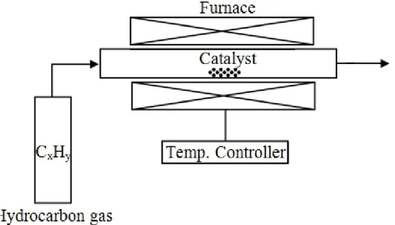
3.1 Hypothesis for mechanisms of CNTs synthesis in CVD. . . 36
3.2 Schematic diagram of a CVD setup in its simplest form. . . 37
3.3 Different synthesized CNTs with different growth temperatures. . . 39
3.4 Schematic illustration shows the use of different diameter iron nanocluster catalysts for the controlled synthesis of carbon nanotubes. . . 40
3.5 Different synthesized CNTs with different gas flow rate. . . 41
3.6 High density of long and aligned CNTs grown on a quartz wafer. . . 43
3.7 Synthesis of DWNTs with different sizes of FeSi2nanoparticles . . . 44
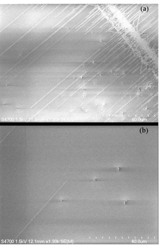
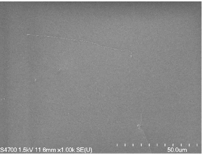
3.8 SEM image of a substrate with proper density of SWNTs. . . 45
3.9 Synthesis of CNTs on pre-etched Si/SiO2substrates . . . 46
3.10 TEM images of a SWNT grown on a pre-etched substrate. . . 47
4.1 Experiment geometry for applying strain and gate voltage with an AFM tip, and measuring conductance with contacts. . . 51
4.3 Schematic of the suspended CNT NEMS device ready forin situTEM imaging. . . 53
4.4 Schematic of back etching processes of device fabrication. . . 55
4.5 Schematic of the macroscopic electrodes deposited onto a wafer by photolithography. . . 55
4.6 Schematic of the alignment of electrodes to the window on the back. . . 56
4.7 Comparison of a CNT connecting two electrodes before and after burn out. . . 56
4.8 Schematic of EBL liftoff process using double-layer PMMA . . . 57
4.9 Comparison of two EBL processes with different sequences of fiducials and patterns. . . 59
4.10 Comparison of a schematic of EBL pattern and the actual result. . . 60
4.11 A SEM image of a device after Si and Si3N4windows beneath the paddles were removed with FIB. . . 61
4.12 SEM images of a sample after CNTs are suspended from the substrate. . . 62
4.13 Schematic of the final structure of the NEMS device. . . 63
4.14 A TEM image of the NEMS device. . . 64
4.15 Schematic of the TEM specimen holder forin situNEMS experiment. . . 65
5.1 Three dimensional schematic of a 4-probe CNT device ready for HRTEM imaging and NBED. . . 71
5.2 Illustration of the diffraction analysis of a SWNT. . . 74
5.3 Comparison between the simulated diffraction pattern and the NBED result of SWNT(38,21). . . 75
5.4 HRTEM image and NBED pattern of a QWNT. . . 76
5.5 NBED pattern of a QWNT with fitted hexagons. . . 77
5.6 Comparison between the simulated diffraction pattern and the NBED result of the QWNT(61,7)@(40,28)@(35,22)@(21,21). . . 81
5.7 The source/drain currentISDversus voltageVSDfor different SWNT devices. . . 83
5.8 Low bias resistanceR=dV dI near zero bias as a function of conducting lengthL. . . 84
5.9 Schematic representation of the main phonon contributions to backscattering. . . 84
5.10 Depiction of the energy dispersion of the metallic SWNTs in the first Brillouin zone and in the vicinity of the Fermi surface. . . 86
5.11 Depiction of the energy dispersion of the semiconducting SWNTs in the vicinity of the Fermi surface. . . 87
6.1 Schematic and TEM images of a telescoping MWNT. . . 93
6.2 SEM images of the twisted CNT device. . . 94
6.3 Band gap change of SWNTs under uniaxial and torsional strains. Notice the linear variation of band gap with the strain and its dependence of the chiral indices. . . 96
6.4 Schematic of the lattice deformation of a twisted CNT. . . 97
6.5 Schematic of the simulated diffraction pattern of a twisted SWNT (22,2). . . 99
6.6 Schematic of the device which is ready for electrical actuation andin situelectron imaging and electron diffraction analysis.. . . 99
6.7 Schematic of the device subject to the uniaxial strain. . . 100
6.8 TEM images and electron diffraction patterns of the suspended DWNT(56,2)@(37,18). The diffraction patterns are false-colored and marked by arrows. . . 102
6.9 TEM images and electron diffraction patterns of the suspended DWNT(65,5)@(24,44). The diffraction patterns are false-colored and marked by arrows. . . 103
6.10 TEM images and NBED patterns of the suspended DWNT(49,18)@(38,16). The diffraction patterns are false-colored and marked by arrows. . . 103
6.11 Comparison between the NBED pattern of a TWNT before and after the twist. . . 105
6.12 The inner shells’ torsional responses to the twist of the outer shell of the four MWNT devices measured. . . 107
6.13 The plot of the ratio of the twist angles in the outer and inner shells θo θi v.s. the corresponding interlayer spacing∆d. . . 107
6.14 Schematic illustration of the suppended CNT with a paddle attached device. . . 108
6.15 The schematic device model and the voltage distribution in FE analysis. . . 109
6.16 Simulated results of the interlayer energy DWNT(10,10)@(5,5)in two models. . . 111
6.17 Simulated results of the interlayer energy DWNT(11,10)@(6,5)in two models. . . 111
6.18 Characterization of DWNT(49,18)@(38,16)and TWNT(7,53)@(8,42)@(11,28) transport properties under torsional strain. . . 113
B.1 Device Fabrication: Backside etching with photolithgraphy . . . 125
B.2 Device Fabrication: Additional Si3N4and SiO2films deposited with PECVD . . . 125
LIST OF ABBREVIATIONS
AFM Atomic Force Microscope BHF Buffered Hydrofluoric Acid CPD Critical Point Drying CNT Carbon Nanotube
CVD Chemical Vapor Deposition DWNT Double-Walled Carbon Nanotube DRIE Deep Reactive Ion Etching EBL Electron Beam Lithography FE Finite Element
FIB Focused Ion Beam
FWNT Few-Walled Carbon Nanotube MEMS Micro-Electromechanical System MWNT Multi-Walled Carbon Nanotube NBD Nano-Beam Diffraction
NEMS Nano-Electromechanical System PMMA Polymethyl Methacrylate RIE Reactive Ion Etching
CHAPTER 1
Introduction to Carbon Nanotubes
1.1
History
Carbon is one of the most recognized and widely used chemical elements in human history. As the sixth element in the periodic table, a free carbon atom has six electrons which occupy1s2,2s2and2p2 atomic orbitals. Due to the small energy level difference between the2pand2sorbitals, the probabilities that four electrons fall into2s,2px,2pyor2pzorbitals could be even and such mixture of2sand2porbitals is called
hybridization. Carbon atom can hybridize insp,sp2orsp3, which can be found in acetylene, polyacetylene or methane, respectively. The property of hybridization distinguishes carbon from other chemical elements, even from group IV elements such as silicon and germanium, because of the absence ofspandsp2hybridizations.
Hybridization is the reason that the physical properties of carbon vary significantly with different allotropic forms, such as graphite, diamond and amorphous carbon, which all have been well known even since antiquity. Although predicted in 1970, it is not until the late twentieth century that another allotrope of carbon was found by Kroto and Smalley asC60[1]. Such a hollow sphere also known as buckyball, stimulated research in the related area. Iijimaet al. [2, 3] first discovered carbon nanotubes in 1991. Shortly after, the variety of intriguing properties of carbon nanotubes attracted tremendous amount of research interest in fundamental science [4, 5, 6, 7, 8].
In this context of dissertation, our research interest will mainly focus on carbon nanotubes. Because carbon nanotubes derive most of the physical properties from graphene, it is reasonable and useful to scrutinize its properties first.
1.2
From Graphene to Carbon Nanotube
Graphene is a one-atom-thick planar sheet ofsp2-bonded carbon atoms in a honeycomb crystal lattice. Bulk graphite is formed by stacking graphene layers over each other. The weak van der Waals interaction between layers makes it easy to slip one layer from another, therefore making the extraction of graphene from a graphite crystal through mechanical/chemical exfoliation possible.
The 2-D graphene lattice can be described by unit vectorsa1anda2, which can be written as:
a1= (a,0), (1.1)
a2=
a 2, √ 3a 2 ! , (1.2)
whereais the lattice constant given bya =√3ac-c, andac-cis the carbon-carbon bond length of 1.44 ˚A.
Correspondingly, basic vectors of the reciprocal latticeb1andb1can be expressed as:
b1=
2π a ,−
2π √
3a
, (1.3)
b2=
0, 4π
2√3a
. (1.4)
Due to the existence of oneπ-electron in eachsp2hybridized carbon atom, there are twoπ-energy bands called bonding and anti-bondingπ-bands in the Brillouin zone of graphene [13, 14]. With the tight binding method, the approximate energy dispersion relation can be derived as:
Egraphene(kx, ky) =±t0
v u u
t1 + 4 cos √
3kxa
2 ! cos k ya 2
+ 4 cos2 k
ya
2
, (1.5)
Figure 1.1: 3D energy dispersion relation of a graphene sheet withπorbital tight binding structure. The Fermi surface consists of six points at the corners of the first Brillouin zone.
at theKpoints through which the Fermi level passes, where theKpoints are the corners of the first Brillouin zone and can be described as
± 4π
3√3a,0
and
± 2π
3√3a,±
2π
3a
, implying that the density of states at the Fermi level is zero. As imposed by the symmetry, the band gaps of graphene at theKpoints are zero, which makes graphene a zero band gap semiconductor, or semi-metal. Also, in the vicinity of theKpoints, according to Equation (1.5), the energy dispersion becomes linear at low energies which leads to massless electrons.
1.3
Structure of Single-Walled Carbon Nanotubes
A single-walled carbon nanotube (SWNT) can be defined as a graphene sheet rolled into a seamless cylindrical shape with helical symmetry, and different ways to wrap up graphene sheets result in SWNTs with different structures. When several tubes with different diameters share the same axis, the structure is named a multi-walled carbon nanotube (MWNT). The smallest diameter of a carbon nanotube was discovered as 0.4 nm [15], while the length of a SWNT goes up to centimeters. This remarkable length-diameter ratio of107makes a carbon nanotube a perfect physics model of one-dimensional material.
The atomic structure of a SWNT is uniquely characterized by the chiral vectorCh=ua1+va2≡(u, v)
Figure 1.2: 1D energy dispersion relation of a graphene sheet. The energy dispersion along the high symmetry directions of the triangleΓM K.
Figure 1.3: Formation of carbon nanotubes on a graphene plane. The chiral vectorCh = ua1+va2of
called chrial indices, as shown in Figure 1.3. Therefore, when rolling up a graphene sheet as a carbon nanotube, the perimeter is determined by the magnitude of the chiral vector, which is:
|Ch|=a
p
u2+v2+uv, (1.6)
while the diameter is:
d= |Ch|
π =
a√u2+v2+uv
π . (1.7)
Once the chiral vector is determined, the translational vectorTcan be obtained in the perpendicular direction to the chiral vector, and can also be defined as the unit vector of a one-dimensional carbon nanotube which is parallel to the nanotube axis.Tshown in the Figure 1.3 is defined as:
T=ma1+na2, (1.8)
wheremandnare integers. SinceCh·T= 0,mandncan be calculated as:
m=−u+ 2v M , n=
2u+v
M (1.9)
whereM is the greatest common divisor ofu+ 2vand2u+v. Hence, the length of the translational vectorT ,i.e.the periodicity of nanotube, is:
|T|=
√
3a√u2+v2+uv
M =
√
3|Ch|
M . (1.10)
On the other hand, since a unit cell is defined by the chiral vectorChand the translational vectorT, the
number of carbon atomsNatomin a unit cell can be shown as:
Natom=|Ch×T|=
4(u2+v2+uv)
M . (1.11)
The angle between the chiral vectorChand the unit vectora1is defined as the chiral angleθ, as shown in
Figure 1.3. The mathematical expression is given by:
θ= arccos Ch·a1
|Ch||a1|
= √ 2u+v
u2+v2+uv. (1.12)
As the result of the helical symmetry of graphene sheet, the value ofθis usually confined in the range
0 ≤θ ≤ π
satisfyu=v, which impliesθ= π
6, such nanotubes are called armchair nanotubes; and ifu >0, v= 0,i.e.
θ= 0, the nanotubes are called zigzag nanotubes; while others are simply called helical/chiral nanotubes. The N-fold rotational symmetry of a nanotube(u, v)can be determined easily using the greatest common divisor of the chiral indicesN = gcd(u, v).
1.4
Energy Dispersion of Single-Walled Carbon Nanotubes
Due to the axial periodicity of a carbon nanotube, the unit cell is defined as the rectangle generated by the chiral vectorChand the translational vectorT. The number of primitive cells per unit cellNcan be calculated
as:
N = |Ch×T|
|a1·a2| =2(u
2+v2+uv)
M . (1.13)
Because there are2Ncarbon atoms in each unit cell, the energy bands are consist ofN pairs ofπbonding bands andπ∗anti-bonding bands.
The reciprocal lattice vectors of a carbon nanotube,K1in the circumferential direction andK2in the
axial direction can be obtained fromRi·Kj =2πδij, whereRiis the lattice vectors in the real space,i.e.
ChandT. Unlike the case of a graphene sheet, the periodic boundary condition along the circumferential
direction quantizes the corresponding wave vector in theChdirection,
Ψk(r+Ch) =eik·ChΨk(r) = Ψk(r), (1.14)
whereas the wave vector inTremains continuous, assuming the length of carbon nanotube is infinite (which is a valid approximation due to the large length/diameter ratio). Therefore, the one-dimensional energy dispersion of a carbon nanotube isNslices of that of graphene. According to Equation (1.5), the energy dispersion of a SWNT is written as:
Eµ(k) =Egraphene
k K2
|K2|+µK1
, µ= 0,1, . . . , N −1;− π
|T| < k < π
|T|. (1.15)
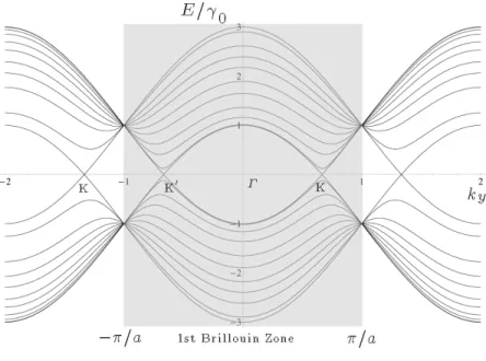
Figure 1.4: Band structure of semiconducting SWNTs. One dimensional energy dispersion relations of SWNTs
Whether a carbon nanotube is metallic or semiconducting can be determined as followed: Because of the Bloch theorem, the periodic boundary conditions in the circumferential direction of a carbon nanotube impose restrictions that,
Φk(r+Ch) =eik·ChΦk(r) = Φk(r). (1.16)
For any vectors kin the vicinity of the Fermi surface, let KF be the Fermi vector, where KF =
1
3(b1−b2) =
0,4π
3
, which yieldsk=KF+δk=
δkx,
4π
3 ky
, whenkis small.
When the chiral indices satisfyu−v= 3l, wherelis an integer, we haveeiKF·Ch = 1,i.e.δk·C
h= 2πq,
withqbeing an integer, which restricts the allowedkvalues by the indexq. Therefore the graphene energy dispersion relationship,
E(kx, ky) =±t0
v u u
t1 + 4 cos √
3kxa
2 ! cos k ya 2
+ 4 cos2 k
ya
2
(1.17)
can now be written as
E(k=KF+δk) =±t0
√
3
2 |δk|. (1.18)
This linear energy dispersion around the Fermi level implies the existence of metallic state with zero band gap whenq= 0with the Fermi velocity ofvF =
√
3at0
2~ .
On the other hand, when the condition ofu−v= 3lis not satisfied,i.e.u−v= 3l±1, we have
δk= 2π
|Ch|
q±1
3
κ⊥+kkκk, (1.19)
whereκ⊥andκkare the basic vectors along the circumferential and the transnational directions. With similar
calculations, the energy dispersion in the vicinity of the Fermi surface is,
Eq±(δk)≈ ± √ 3a 2 t0 s 2π |Ch|
2 q±1
3
2
+k2
k. (1.20)
Now at the Fermi surface,i.e.kk= 0, the energy difference between the two nearest subbands, which are
both defined byq= 0, can be expressed as,
Eq+=0(kk= 0)−Eq−=0(kk= 0) = 2πat0 √
3|Ch|
In other words, the energy band gap in a semiconducting carbon nanotube in the zone-folding approxima-tion can be expressed as
Eg0=at0
r , (1.22)
whereris the carbon nanotube radius.
As expected, a very large diameter carbon nanotube can be analyzed as a zero-gap semiconductor similar to a graphene sheet. This inverse linear energy dispersion at the Fermi surface was first discovered by White and Mintmire [16]. However, such model is in the first order approximation and unable to describe the actual energy dispersion for carbon nanotubes dealt as planar sheets while ignoring the curvature effects. Since when wrapping a graphene sheet to a carbon nanotube, the topology will change both the directions and the bond lengths of the basic vectorsa1anda2. Furthermore, in the tight binding analysis of graphene, the behaviors
of electrons are described using the independentπstates. Given that the planar symmetry is broken in a carbon nanotube, theπstates are mixed withσstates and the orbitals exhibit bothsp2andsp3characters. As consequences, besides the radius, the band structure of a carbon nanotube also depends on the specific chirality,
Eg1= 3t0a
2
c-c
16r2 cos 3θ, (1.23)
whereθis the chiral angle. The secondary band gap scaled by 1
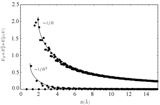
r2 will become dominant for carbon nanotubes with small diameters, whereas negligible for large ones and particularly armchair carbon nanotubes where the chiral angle is 30◦. In this study, most synthesized SWNTs and MWNTs are of diameters around 5 nm, therefore the secondary band gaps in the order of 1 meV are negligible compared with the zone-approximation induced band gaps, which are normally 0.1 - 0.2 eV [17].
1.5
Multi-Walled Carbon Nanotubes
A MWNT consists of a nested concentric array of SWNT constituents, separated from one another by approximately 3.4 ˚A, which is also the interlayer spacing of graphene sheets in graphite. Similar to a SWNT, the individual layers of a MWNT can be entirely defined by chiral indices(u, v), and the MWNT is usually represented as(u1, v1)@(u2, v2)@. . .@(ui, vi)@. . ., whereuiandviare the chiral indices of thei-th shell.
Figure 1.5: Correlation between the band gap of carbon nanotubes and the radii. The band gaps of semi-conducting (top) and metallic (bottom) nanotubes as a function of tube radius. The solid lines are guide to the eye showing that the primary zone-approximation band gapE0gscales a1/r,and the curvature induced
hybridization secondary band gapE1
gscales as1/r2. NoticeEg1is significant only for small metallic tubes
dominated by the chiral indices(u, v)of the constituent tubes, and each spacing can be accurately calculated once the structure of a MWNT is known.
Due to the complexity of a multi-walled system and interwall interactions, the band structure of a MWNT cannot be simply treated as the superposition of each individual SWNTs, the symmetry or the commensuration, however, plays a significant role in determining the band structure, as illustrated in Figure 1.6. A MWNT is commensurate if the ratio of the translational vectors|T|of two consecutive layers is a rational number,
e.g.a DWNT(5,5)@(10,10); otherwise incommensurate,e.g.a DWNT(5,5)@(9,9). The high symmetry in a commensurate MWNT suggests a periodic system with significant interlayer coupling. Figure 1.6 illustrates the differences in a commensurate DWNT(5,5)@(10,10)induced by symmetry and interlayer interactions. The coupling strength between the nearest-neighboring carbon atoms in incommensurate layers is not translationally invariant along the axial direction, therefore the periodicity is lost and the interlayer coupling is much weaker than in a commensurate case, and in this case the band structure of a MWNT can be approximated as the composition of each constituent SWNTs.
Figure 1.6: Differences of band structure of a commensurate DWNT(5,5)@(10,10)induced by symmetry and interlayer interaction. (a) shows the simple superposition of the band structures of two armchair SWNTs
(5,5)and(10,10). By introducing interlayer interaction, the band structure shifts a little in (b) while the DWNT remains metallic. However, if the symmetry of such coaxial system is broke by changing the relative angular position between outer and inner shells, a pseudo-gap open as shown in (c).
between the neighboring shells due to the change of symmetry, as shown in Figure 1.6. The dependence of the ground state energy of a DWNT has been formulated with respect to the interlayer spacing and the chiral angle difference [21], and the dependence on chiral angles turns out to be weak.
1.6
Mechanical Properties of Carbon Nanotubes
Since the discovery of carbon nanotubes, much attention has been paid to the mechanical properties, especially the elastic response to stress. Using molecular dynamics simulation with Tersoff-Brenner potential for the carbon-carbon interaction, Robertsonet al. [22] first calculated the Young’s modulus of nanotubes as smaller than that of graphene. Lu [23] calculated the Young’s modulus for both SWNTs and MWNTs, and claimed that the values are around 1.0 TPa with an empirical force-constant model, which are insensitive to the chirality, the tube size, and the number of walls, and comparable to that of graphene. These results were confirmed in subsequent studies with other approaches including the tight-binding simulation and density-functional calculation [24, 25], the Born’s perturbation technique within a lattice-dynamical model [26], as well as a modified Morse potential[27] and MM3 potential [28] .
With the Tersoff-Brenner potential, Yakobsonet al. [29] and Kudinet al. [30] predicted the Young’s modulus of 5.5 and 3.86 TPa using continuum elasticity theory. However these values were derived basing on an assumption that the individual wall thickness is of the size of molecular orbital radius. If the inter-wall van der Waals distance is used instead, the Young’s modulus is about 1 TPa, which then becomes consistent with other calculations. Table 1.1 summarizes the elastic moduli calculated using various methods. With few exceptions the generally agreed value for the Young’s modulus is around 1 TPa.
Table 1.1: Values of Young’s and shear moduli of carbon nanotubes calculated by various groups with different methods. Young’s moduli are on the order of 1 TPa. In Yakobsonet al., if the interlayer spacing of 3.4 ˚A, rather thanπ-bond length 0.66 ˚A, is used for van der Waals energy calculation, one obtains the Young’s modulus of 1.07 TPa, which is consistent with other calculations.
Author Year Young’s Modulus Shear Modulus Method
(TPa) (TPa)
Robertsonet al. [22] 1992 1.06 Tersoff-Brenner Yakobsonet al. [29] 1995 5.5 Tersoff-Brenner
Cornwell and Wille [34] 1997 1 Tersoff-Brenner
Lu [23] 1997 0.97 0.45 Force-constant
Hernandezet al. [24] 1998 1.24 Density Function Krishnanet al. [35] 1998 1.3 Thermal Vibration Sanchez-Portalet al. [25] 1998 1.05 Density Function
Popovet al. [26] 1999 1.00 0.41 Lattice Dynamics Ozakiet al. [36] 2000 0.98 O(n) Tight binding
Van Lieret al. [37] 2000 1.09 Hartree-Fock
Belyschkoet al. [27] 2002 0.94 Modified Morse Li and Chou [31] 2003 1.06 0.44 Energy Approach
Pullenet al. [38] 2004 1.1 GGA
BIBLIOGRAPHY
[1] H. W. Kroto, J. R. Heath, S. C. O’Brien, R. F. Curl, and R. E. Smalley, “C 60: buckminsterfullerene,”
Nature, vol. 318, no. 6042, pp. 162–163, 1985.
[2] S. Iijimaet al., “Helical microtubules of graphitic carbon,”Nature, vol. 354, no. 6348, pp. 56–58, 1991. [3] S. Iijima and T. Ichihashi, “Single-shell carbon nanotubes of 1-nm diameter,”Nature, vol. 363, no. 6430,
pp. 603–605, 1993.
[4] S. J. Tans, A. R. Verschueren, and C. Dekker, “Room-temperature transistor based on a single carbon nanotube,”Nature, vol. 393, no. 6680, pp. 49–52, 1998.
[5] W. A. De Heer, A. Chatelain, and D. Ugarte, “A carbon nanotube field-emission electron source,”Science, vol. 270, no. 5239, pp. 1179–1180, 1995.
[6] A. Javey, J. Guo, Q. Wang, M. Lundstrom, and H. Dai, “Ballistic carbon nanotube field-effect transistors,”
Nature, vol. 424, no. 6949, pp. 654–657, 2003.
[7] S. Frank, P. Poncharal, Z. Wang, and W. A. de Heer, “Carbon nanotube quantum resistors,”Science, vol. 280, no. 5370, pp. 1744–1746, 1998.
[8] R. A. Martel, T. Schmidt, H. Shea, T. Hertel, and P. Avouris, “Single-and multi-wall carbon nanotube field-effect transistors,”Applied Physics Letters, vol. 73, p. 2447, 1998.
[9] K. Novoselov, A. K. Geim, S. Morozov, D. Jiang, Y. Zhang, S. Dubonos, I. Grigorieva, and A. Firsov, “Electric field effect in atomically thin carbon films,”Science, vol. 306, no. 5696, pp. 666–669, 2004. [10] K. Novoselov, A. K. Geim, S. Morozov, D. Jiang, M. K. I. Grigorieva, S. Dubonos, and A. Firsov,
“Two-dimensional gas of massless dirac fermions in graphene,”Nature, vol. 438, no. 7065, pp. 197–200, 2005.
[11] Y. Zhang, Y.-W. Tan, H. L. Stormer, and P. Kim, “Experimental observation of the quantum hall effect and berry’s phase in graphene,”Nature, vol. 438, no. 7065, pp. 201–204, 2005.
[12] A. C. Neto, F. Guinea, N. Peres, K. Novoselov, and A. Geim, “The electronic properties of graphene,”
Reviews of Modern Physics, vol. 81, no. 1, p. 109, 2009.
[13] P. Wallace, “The band theory of graphite,”Physical Review, vol. 71, no. 9, p. 622, 1947.
[14] M. Anantram and F. Leonard, “Physics of carbon nanotube electronic devices,”Reports on Progress in Physics, vol. 69, no. 3, p. 507, 2006.
[15] L.-C. Qin, X. Zhao, K. Hirahara, Y. Miyamoto, Y. Ando, and S. Iijima, “Materials science: The smallest carbon nanotube,”Nature, vol. 408, no. 6808, pp. 50–50, 2000.
[16] J. Mintmire and C. White, “Universal density of states for carbon nanotubes,”Physical Review Letters, vol. 81, no. 12, pp. 2506–2509, 1998.
[17] J.-C. Charlier, X. Blase, and S. Roche, “Electronic and transport properties of nanotubes,”Reviews of Modern Physics, vol. 79, no. 2, p. 677, 2007.
[18] A. N. Kolmogorov and V. H. Crespi, “Smoothest bearings: interlayer sliding in multiwalled carbon nanotubes,”Physical Review Letters, vol. 85, no. 22, pp. 4727–4730, 2000.
[20] A. Hashimoto, K. Suenaga, K. Urita, T. Shimada, T. Sugai, S. Bandow, H. Shinohara, and S. Iijima, “Atomic correlation between adjacent graphene layers in double-wall carbon nanotubes,”Physical Review
Letters, vol. 94, no. 4, p. 045504, 2005.
[21] L. Bellarosa, E. Bakalis, M. Melle-Franco, and F. Zerbetto, “Interactions in concentric carbon nanotubes: The radius vs the chirality angle contributions,”Nano Letters, vol. 6, no. 9, pp. 1950–1954, 2006. [22] D. Robertson, D. Brenner, and J. Mintmire, “Energetics of nanoscale graphitic tubules,”Physical Review
B, vol. 45, no. 21, p. 12592, 1992.
[23] J. P. Lu, “Elastic properties of carbon nanotubes and nanoropes,”Physical Review Letters, vol. 79, no. 7, pp. 1297–1300, 1997.
[24] E. Hernandez, C. Goze, P. Bernier, and A. Rubio, “Elastic properties of c and b {x} c {y} n {z} composite nanotubes,”Physical Review Letters, vol. 80, no. 20, pp. 4502–4505, 1998.
[25] D. S´anchez-Portal, E. Artacho, J. M. Soler, A. Rubio, and P. Ordej´on, “Ab initio structural, elastic, and vibrational properties of carbon nanotubes,”Physical Review B, vol. 59, no. 19, p. 12678, 1999. [26] V. Popov, V. Van Doren, and M. Balkanski, “Elastic properties of single-walled carbon nanotubes,”
Physical Review B, vol. 61, no. 4, p. 3078, 2000.
[27] T. Belytschko, S. Xiao, G. Schatz, and R. Ruoff, “Atomistic simulations of nanotube fracture,”Physical Review B, vol. 65, no. 23, p. 235430, 2002.
[28] A. Sears and R. Batra, “Macroscopic properties of carbon nanotubes from molecular-mechanics simula-tions,”Physical Review B, vol. 69, no. 23, p. 235406, 2004.
[29] B. I. Yakobson, C. Brabec, and J. Bernholc, “Nanomechanics of carbon tubes: instabilities beyond linear response,”Physical Review Letters, vol. 76, no. 14, pp. 2511–2514, 1996.
[30] K. N. Kudin, G. E. Scuseria, and B. I. Yakobson, “C {2}f, bn, and c nanoshell elasticity from ab initio computations,”Physical Review B, vol. 64, no. 23, p. 235406, 2001.
[31] C. Li and T.-W. Chou, “Elastic moduli of multi-walled carbon nanotubes and the effect of van der waals forces,”Composites Science and Technology, vol. 63, no. 11, pp. 1517–1524, 2003.
[32] L. Shen and J. Li, “Transversely isotropic elastic properties of multiwalled carbon nanotubes,”Physical Review B, vol. 71, no. 3, p. 035412, 2005.
[33] B.-W. Jeong, J.-K. Lim, and S. B. Sinnott, “Elastic torsional responses of carbon nanotube systems,”
Journal of Applied Physics, vol. 101, no. 8, pp. 084309–084309, 2007.
[34] C. Cornwell and L. Wille, “Elastic properties of single-walled carbon nanotubes in compression,”Solid State Communications, vol. 101, no. 8, pp. 555–558, 1997.
[35] A. Krishnan, E. Dujardin, T. Ebbesen, P. Yianilos, and M. Treacy, “Youngs modulus of single-walled nanotubes,”Physical Review B, vol. 58, no. 20, p. 14013, 1998.
[36] T. Ozaki, Y. Iwasa, and T. Mitani, “Stiffness of single-walled carbon nanotubes under large strain,”
Physical Review Letters, vol. 84, no. 8, pp. 1712–1715, 2000.
[37] G. Van Lier, C. Van Alsenoy, V. Van Doren, and P. Geerlings, “Ab initio study of the elastic properties of single-walled carbon nanotubes and graphene,”Chemical Physics Letters, vol. 326, no. 1, pp. 181–185, 2000.
[38] A. Pullen, G. Zhao, D. Bagayoko, and L. Yang, “Structural, elastic, and electronic properties of deformed carbon nanotubes under uniaxial strain,”Physical Review B, vol. 71, no. 20, p. 205410, 2005.
CHAPTER 2
Characterization of Carbon Nanotubes
Understanding the atomic structure of carbon nanotubes(CNTs) is essential for further investigation of the physical properties. Various techniques have been applied to characterize the structure,i.e. the chiral indices, of CNTs. For example, transmission electron microscopy (TEM), scanning tunneling microscopy (STM), scanning electron microscopy (SEM), atomic force microscope (AFM), X-ray diffraction (XRD), Raman spectroscopy, optical absorption spectroscopy, and nuclear magnetic resonance (NMR) have all been used for the characterization with emphasis on different requirements. Among those techniques, it has been a consensus that TEM is the most accurate and powerful one for characterizing CNT structure. Meanwhile, other techniques are also widely used despite their intrinsic limitations.
2.1
Scanning Tunneling Microscopy and Other Techniques
A scanning tunneling microscope (STM) is an instrument based on the concept of quantum tunneling, which provides a high resolution up to 1 ˚A. When the metal probe of a STM is brought to the vicinity of sample surface, a bias voltage is applied between the probe and the surface which induces a tunneling current. The magnitude of this current depends on the geometry of the probe as well as local density of states (DoS) of the surface. Therefore, through monitoring the tunneling current, the DoS can be derived and the surface morphology is obtained. Both the atomic structure and the electronic properties of SWNTs have been experimentally measured using STM [1, 2, 3], as shown in Figure 2.1.
Despite the high resolution of a STM, the structural deformation [4, 5] caused by the interaction between a CNT and the substrate induces considerable errors in STM measurement. Besides, the interlayer interaction shadows most information of the inner tubes in a MWNT. Thus, STM technique is unable to detect the complete atomic structure of a MWNT [6]. Giuscaet al. [7] demonstrated that the chirality of the inner shell in a DWNT can be obtained from the STM measurement combined with calculated local DoS. However, the method works only in certain combinations of inner and outer shells and thus can not be universally applied to all MWNTs.
As a successor of STM, an atomic force microscopy (AFM) shares the similar mechanism except using a cantilever with a sharp tip as the probe, which actually in contact with the surface and accurately manipulated with piezoelectric element [8]. Although the lateral resolution is in the order of fraction of nanometer, an AFM only allows one to observe the diameter of a CNT instead of the detailed chiral structure.
Raman spectroscopy is another widely used technique for the study of vibrational, rotational, and other low frequency modes in materials. The diameter dependence of vibrational mode frequencies and the electronic structure of CNTs can be studied by Raman spectroscopy. The energy of interband transition can be obtained from resonance Raman scattering (RRS). A plot of transition energies of all chiral structures calculated from tight-binding model should be compared with those obtained from RRS experiments. With the tube diameter, the chiral indices can be determined by a match between theoretical and measured transition energies[9, 10]. However, the signals become very weak and are broadened for SWNT with large diameter and MWNTs. This is because that the curvature of CNT has less influences and the Raman spectra resemble to that of graphene when the diameter is large. Only the diameter information can be obtained using these two techniques, which is usually not enough to identify the chirality of CNTs [11, 12].
SEM images a sample by scanning the surface with a focused beam of electrons and detecting the secondary electrons to obtain the information of surface topography. In the applications to CNTs, SEM is usually used to determine the macroscopic shapes. Although the resolution of SEM is in the order of 2 nm, the accumulation of electrons on the nonconductive substrate causes image artifacts during scanning and imposes difficulties for accurate imaging.
2.2
Transmission Electron Microscopy and Nano-Beam Electron Diffraction
at a prominent higher resolution, theoretically smaller than 1 ˚A, than previous techniques. It is then possible to characterize material structures at the atomic level. However, the imperfection of the magnetic lenses, which are designed to focus fast electrons in desired direction, restricts the highest resolution to about 1 ˚A[13]. On the other hand, CNTs, especially SWNTs, are quite vulnerable to high energy electrons. As shown by Smith
et al. [14] that, the threshold voltage of knock-on damage on a SWNT is around 86 keV. Thus in order to preserve CNTs from incomplete structures during the imaging, the energy of electrons is usually limited to 100 keV.
2.2.1
Mechanism of Transmission Electron Microscopy
A TEM [15, 16] produces an image based on the following two-step Abbe principle:
• The incident electrons are scattered by the specimen and form a diffraction pattern on the back focal plane of the objective lens;
• The scattered electrons are recombined to form an image on the image plane.
Two imaging mechanisms are usually used: amplitude contrast and phase contrast [17]. In the amplitude contrast mode, the image contrast is the result from the electrons scattered in different angles within a specimen. The areas of the specimen with higher mass or larger Coulomb potential will scatter more electrons toward large angles. If a small aperture is used, most electrons which are scattered in large angles can be excluded except the selected beam inside the aperture. As a result, the areas corresponding to the higher mass or strong atomic potential positions within the specimen will turn dark in the image. On the other hand, image contrast in the phase contrast mode comes from the phase difference of electrons caused by interactions between electrons and the Coulomb potential of the specimen. A large objective aperture is usually used to allow more scattered beams to pass through the objective lens to form an image. It offers a much higher structural resolution and is usually called high resolution TEM compared to the amplitude contrast mode, but it requires that the specimen be thin.
For phase contrast imaging, the interactions between the incident electrons and the specimen are usually weak and theories can be greatly simplified. In the phase-grating approximation, the wave function of the electrons scattered by specimen can be described [18],
Ψo(x, y) = e−iβVp(x,y), (2.1)
whereβ = π
the incident electron beam andλis the wave length of the electrons. For a thin specimen constituted of light atoms, the weak phase object approximation can be applied and Equation (2.1) can be simplified to,
Ψo(x, y)'1−iβVp(x, y), (2.2)
where the unit1represents the transmitted wave which has no interaction with the specimen and the imaginary part corresponds to the scattered waves. The image wave on the image plane is a convolution of the object wave and the contrast transfer functionT(r):
Ψi(r) = Ψo(r)⊗T(r), (2.3)
where⊗is the convolution operator. The convolution operation of two functions can be expressed as the product of their corresponding Fourier transforms in reciprocal space:
ˆ
Ψi(q) = ˆΨo(q)·Tˆ(q). (2.4)
The contrast transfer function in a TEM includes the information of aperture function, spherical aberration and imperfection of focusing of the objective lens and is given by:
T(q) =a(q)e2iπχ(q), (2.5)
wherea(q)is the aperture function of the objective lens and
χ(q) = 1 4Csλq
4+1
2∆f q
2,
(2.6)
where Cs and∆f are the spherical aberration coefficient and defocus of the objective lens, respectively.
Equation (2.2) can be arranged as:
Ψi(x, y) = 1 +βVp(x, y)⊗ <[T(x, y)]−iβVp(x, y)⊗ =[T(x, y)], (2.7)
where<[T(x, y)]and=[T(x, y)]are the real and imaginary part ofT(x, y), respectively. In the weak phase object approximation, whereβVp1, the image intensity can be further simplified as:
2.2.2
Imaging of Carbon Nanotubes in the Real Space with TEM
Due to the low atomic number of carbon, it is valid to apply the weak phase object approximation to interpret the TEM images of the structures [19]. Theoretically, a high resolution of 2 ˚Acan be reached using a TEM with a field emission electron gun, while the quality and the resolution of imaging are limited by thermal and mechanical vibrations, stage drift and instability of the magnetic lenses.
Figure 2.2: TEM images of CNTs. (a) a SWNT, (b) a DWNT and (c) a six-walled CNT. Pictures were captured with JOEL 2010F at 80 kV.
When imaging a SWNT in the real space [20], due to the scattering of electrons at carbon atoms, the tube walls spread out as paired dark lines. Even in the best scenario, a simple measurement of the distance between a pair of walls, corresponding to the tube diameter, is subject to systematic and substantial deviations from the true value due to the inevitable Fresnel fringes arising at the edges of the nanotubes. The diameter measurement is definitely 0.1 nm smaller than the true value provided certain experimental condition. In the case of a MWNT, it is more complicated to measure the diameters of the constituent tubes because of the more intense interference of Fresnel fringes. Hence, the interlayer spacing tends to appear brighter due to the interference, and the interlayer distance is likely to be overestimated [21].
2.2.3
Theory of Electron Diffraction of Carbon Nanotubes
Figure 2.3: Simulated high resolution image of a(4,4)SWNT: (A) Atomic model and (B) corresponding projected potential along the incident electron beam direction for a(4,4)SWNT. The simulation in TEM is shown in (C), where the two walls appear as the dark lines [21].
in 1996 [23], the CNT electron diffraction theory has proved to be the most powerful method to characterize fine structures of CNTs [24, 25, 26, 27, 28].
The diffraction pattern of a CNT should be based on that of a graphene, which is the six-fold symmetrical honeycomb. However, the periodicity introduced by the circumferential confinement significantly distinguishes the diffraction pattern of a CNT.
The convenience of using cylindrical coordinates(r, φ, z)encourages us to express the atomic structure of a CNT(u, v)asvpairs of helices parallel toa1. Therefore in a unit cell, there are
2(u2+v2+uv)
M v atoms in each helix. We can choose the position of an arbitrary atom as the origin(r0, φ0, z0), then we have,
r=r0 φ1
j = 2πj
acosθ |Ch|
,
z1
j =−jasinθ.
(2.9)
r=r0,
φ2j = 2πjacosθ |Ch|
−2π a0cos(
π
6 +θ)
√
3|Ch|
,
z2
j =−jasinθ+
asin(π 6 +θ)
√
3 .
(2.10)
Note that there are three equivalent representations of helices in a CNT depending on different crystallo-graphic directions,a1,a2ora3=a2−a1. And the position of atoms can be expressed in similar manners in
different representations.
It can be expected that due to the existence of multiple helices and cylindrical confinement, compared with the honeycomb-like diffraction patterns of graphene, the diffraction patterns of a CNT will no longer be single spots but distribute in a manner of Bessel functions.
On the other hand, the periodicities in the real space will also be reflected in the diffraction patterns. If we define the spacing between the neighboring atoms on a helix as∆, the pitch length of a helix asCand the spacing between unit cells asc, the corresponding periodicities of 1
∆, 1
c and
1
C should be observed in the diffraction pattern, as illustrated in Figure 2.4.
Figure 2.4: Schematic of periodicities in the real spacec, Cand∆of a CNT with the corresponding diffraction patterns. [27]
F(q) = 2πme
h2 Z
U(r)e2iπq·rdr, (2.11)
whereU(r)is the Coulomb potential of the scattering atom;eandmare the charge and the relativistic mass of electron;his Plank’s constant andqis the scattering vector with the magnitude defined as
|q|=2 sin(Θ/2)
λ , (2.12)
whereΘis the total scattering angle andλis the wave length of the incident electron.
Considering a continuous helix, we can express Equation (2.11) in cylindrical coordinates using Equa-tion (2.9) and EquaEqua-tion (2.10),
F(R,Φ, Z) =
Z
V(r) exp(2πiq·r) dr
=
Z ∞
−∞
Z 2π 0
Z ∞
0
V(r, φ, z) exp[2πirRcos(φ−Φ)] exp(2πizZ)rdrdφdz, (2.13)
where (r, φ, z) and (R,Φ, Z) are the cylindrical coordinates in the real space and the reciprocal space, respectively;V(r, φ, z) = 2πme
h2 U(r)is the modified scattering potential. Bessel functions can be defined as,
eizcosθ=
+∞
X
n=−∞
Jn(z) exp
h
inθ+π 2
i
, (2.14)
with the property of,
J−n(z) = (−1)nJn(z). (2.15)
Plug the both relationships into Equation (2.13),
F(R,Φ, Z) =X
n
Z ∞
−∞
Z ∞
0
V(r, φ, z) exp(inΦ)
× (
Z 2π 0
+∞
X
n=−∞
Jn(2πrR) exp
h
inΦ−φ+π 2
i
dφ )
exp(2πizZ)rdrdφdz (2.16)
V(r, φ, z) =X
n
VnN(r, z) exp(−inN φ)
=
+∞
X
n=−∞
+∞
X
l=−∞
Vnl(r) exp
−inφ+2πilz
c
. (2.17)
By incorporating the z-components into Equation (2.16), the structure factor becomes,
F(R,Φ, l) = 1
c
∞
X
n=1
ein(Φ+π/2),
× Z c
0 Z 2π
0 Z ∞
0
V(r, φ, z)Jl(2πrR)ei(−nφ+2πlz/c)rdrdφdz. (2.18)
Immediately, the constant potential of a continuous helix with a radius ofroand a pitch lengthCis given
as,
V(r, φ, z) =Voδ(r−ro)δ(
2πz
C −φ). (2.19)
Substitute the modified potential into Equation (2.18), the scattering amplitude of one continuous helix is now:
F(R,Φ, l) =roVoJl(2πroR) exp[i(Φ +π/2)l]. (2.20)
Given a SWNT withjatoms on the helix, the structure factor can be given as,
F(R,Φ, l) =X
n
ein(Φ+π/2)Jn(2πrR)
X
j
fjei(−nφj+2πljz/c). (2.21)
wherefjis the atomic scattering amplitude of thej-th carbon atom,(r, φj, lj)are the cylindrical coordinates,
andnis the integer which is allowed by the selection rule. Note that, the different periodicities of a SWNT in the real space, such as neighboring molecular group spacing∆, helices pitch lengthCand periodicity of structurec, imply repeated diffraction patterns in reciprocal space with periodicities of 1
∆, 1
C, and
1
c, respectively. This gives the selection rule,
l c =
n C+
m
Given a SWNT of(u, v), the pitch length isC =|Ch|tan(
π
3 −θ), while the neighboring molecular
group spacing∆ =asin(π
3 −θ), and the axial periodicity|T|=
√
3|Ch|
M , therefore Equation (2.21) can be re-arranged for the exact value ofl.
Meanwhile, by plugging the coordinates of carbon atoms of a SWNT to Equation (2.22), the structure factor of a SWNT(u, v)can finally be expressed as,
Fuv(R,Φ, l) =
X
n,m
f γuv(n, m)χuv(n, m)Jn(πdR) exp
h
inΦ +π 2
i
, (2.23)
where
χuv(n, m) = 1 + exp
2πi
−n+ (u+ 2v)m
3v
, (2.24)
and
γuv(n, m) =
v when[n+ (u+v)m]/v=N
0 otherwise
(2.25)
From the above expressions, the structure factor can be divided into two parts:
1. reflections of graphene lattice,
X
n,m
γuv(n, m)χuv(n, m). (2.26)
2. curvature effects,
X
n,m
Jn(πdR) exp
h
inΦ +π 2
i
. (2.27)
The intensity distribution of diffraction patterns is computed by
Iuv=|Fuv(R,Φ, l)|2. (2.28)
2.2.4
Determination of Chiral Structure of a Carbon Nanotube
labeled asl1, l2,andl3. The elongation of the diffraction spots perpendicular to the tubule axis is due to a lack of translational periodicity in this direction. As we can see from the image, the peak of intensity is shifted because of the curvature of the CNT [29].
The intensity distribution on the equatorial layer line is dominated by the0-th order Bessel function, whereas the allowed values oflare constrained by the selection rule that,
l=n2u+v M v +m
2(u2+v2+uv)
M v , (2.29)
wherenandmare integers. Equation (2.29) gives the lowest order of Bessel function for the principal lines l1, l2andl3are−v, uand−(u+v), respectively. Furthermore, each principal line consists of an infinite series of Bessel functions, the orders of which increase in the step of 2(u
2+v2+uv) M . Since
2(u2+v2+uv)
M is
usually a large number and the magnitudes of the high order Bessel functions are negligible, only the Bessel function of the lowest order is significant. Therefore
I(R,Φ, l1)∝|Jv(πdR)|2, (2.30)
I(R,Φ, l2)∝|Ju(πdR)|2, (2.31)
I(R,Φ, l3)∝|Ju+v(πdR)|2. (2.32)
Hence, with the knowledge of the intensity distribution on any two principal layer lines, the chiral indices
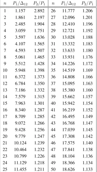
(u, v)can be accurately identified. According to the characteristics of the Bessel functionJv, the ratio of the
positions of first two peaksP2
P1 in the intensity profile uniquely depends on the orderv, therefore it provides another possibility to determine the chiral indices. While in practice, because of the distraction of inevitable background noises and possible contaminations, it is difficult to accurately locate the position of peaks in the intensity distributions. Whereas the “valleys” on the primary lines, which corresponding to the roots of Bessel function, are much more distinguishable due to the zero intensity. For a certain order Bessel function, the distance between the first pair of roots2P1and the interval spacing∆12between the first two roots are also unique [30], as illustrated in Figure 2.6. Hence, both the ratios of P2
P1 and P1
∆12
can be used to evaluate the order of Bessel function. The correlation between them can be found in Table 2.1.
Table 2.1: Characteristic ratioP2/P1,P1/∆12for Bessel function of orders from 0 to 50. n P1/∆12 P2/P1 n P1/∆12 P2/P1
lines to the equatorial line can be expressed as
D1=|b|sin( π
2 −θ), (2.33)
D2=|b|sin(π
6 +θ), (2.34)
D3=|b|sin(π
6 −θ). (2.35)
where bis the unit vector of the graphene lattice in reciprocal space. Note that, the chiral angle is also expressed in Equation (1.12). The ratio of chiral indices are then deduced as,
v u=
2D2−D1
2D1−D2
. (2.36)
Although instead of the individual chiral indices, only the ratio can be obtained with this method, the independent measurements ofD1, D2, andD3are more discernible and thus provide higher error tolerance. Figure 2.7 shows the simulations of the diffraction patterns of SWNTs(11,5)and(50,11), due to the smaller diameter, the peaks on each principle lines of(11,5)are more spread and easier to locate, whereas the errors when reading the intensity distribution of the larger SWNT(50,11)are considerable. However, the line spacings betweenD1, D2, andD3can always be determined with relatively small errors. Therefore, the method of measuring the spacing of the principal layer lines are preferred and usually combined with the diameter measurement from TEM imaging in the real space to unambiguously determine the chiral structure.
The characterization of chiral structure of a SWNT from the diffraction pattern in practice can be generalized in the following steps:
1. Capture the image of the SWNT in the real space and the diffraction pattern in the reciprocal space at a relative low acceleration voltage;
2. Measure the diameter in the real space imagedreal, note that the deviation from the true value;
3. Locate at least three primary layer lines and therefore at least two line spacings. Plug the spacings into Equation (2.36) to find possiblev/uratio;
4. Measure the positions of peaks and valleys on at least one discernible primary layer line and look up the order of corresponding Bessel function.
BIBLIOGRAPHY
[1] J. W. Wilder, L. C. Venema, A. G. Rinzler, R. E. Smalley, and C. Dekker, “Electronic structure of atomically resolved carbon nanotubes,”Nature, vol. 391, no. 6662, pp. 59–62, 1998.
[2] T. W. Odom, J.-L. Huang, P. Kim, and C. M. Lieber, “Atomic structure and electronic properties of single-walled carbon nanotubes,”Nature, vol. 391, no. 6662, pp. 62–64, 1998.
[3] A. Hassanien, M. Tokumoto, Y. Kumazawa, H. Kataura, Y. Maniwa, S. Suzuki, and Y. Achiba, “Atomic structure and electronic properties of single-wall carbon nanotubes probed by scanning tunneling micro-scope at room temperature,”Applied Physics Letters, vol. 73, no. 26, pp. 3839–3841, 1998.
[4] T. Hertel, R. E. Walkup, and P. Avouris, “Deformation of carbon nanotubes by surface van der waals forces,”Physical Review B, vol. 58, no. 20, p. 13870, 1998.
[5] E. W. Wong, P. E. Sheehan, and C. M. Lieber, “Nanobeam mechanics: elasticity, strength, and toughness of nanorods and nanotubes,”Science, vol. 277, no. 5334, pp. 1971–1975, 1997.
[6] A. Rubio, “Spectroscopic properties and stm images of carbon nanotubes,”Applied Physics A, vol. 68, no. 3, pp. 275–282, 1999.
[7] C. E. Giusca, Y. Tison, V. Stolojan, E. Borowiak-Palen, and S. R. P. Silva, “Inner-tube chirality deter-mination for double-walled carbon nanotubes by scanning tunneling microscopy,”Nano Letters, vol. 7, no. 5, pp. 1232–1239, 2007.
[8] S. J. Tans, A. R. Verschueren, and C. Dekker, “Room-temperature transistor based on a single carbon nanotube,”Nature, vol. 393, no. 6680, pp. 49–52, 1998.
[9] A. Jorio, R. Saito, J. Hafner, C. Lieber, M. Hunter, T. McClure, G. Dresselhaus, and M. Dresselhaus, “Structural (n, m) determination of isolated single-wall carbon nanotubes by resonant raman scattering,”
Physical Review Letters, vol. 86, no. 6, pp. 1118–1121, 2001.
[10] H. Telg, J. Maultzsch, S. Reich, F. Hennrich, and C. Thomsen, “Chirality distribution and transition energies of carbon nanotubes,”Physical Review Letters, vol. 93, no. 17, p. 177401, 2004.
[11] J. Benoit, J. Buisson, O. Chauvet, C. Godon, and S. Lefrant, “Low-frequency raman studies of multiwalled carbon nanotubes: Experiments and theory,”Physical Review B, vol. 66, no. 7, p. 073417, 2002. [12] X. Zhao, Y. Ando, L.-C. Qin, H. Kataura, Y. Maniwa, and R. Saito, “Radial breathing modes of
multiwalled carbon nanotubes,”Chemical Physics Letters, vol. 361, no. 1, pp. 169–174, 2002.
[13] D. C. Joy and A. D. Romig Jr, Principles of analytical electron microscopy. Plenum Publishing Corporation, 1986.
[14] B. W. Smith and D. E. Luzzi, “Electron irradiation effects in single wall carbon nanotubes,”Journal of Applied Physics, vol. 90, no. 7, pp. 3509–3515, 2001.
[15] D. B. Williams and C. B. Carter,The Transmission Electron Microscope. Springer, 1996.
[16] L. Reimer and H. Kohl,Transmission electron microscopy: physics of image formation, vol. 36. Springer Verlag, 2008.
[17] H. Deniz,Electron diffraction and microscopy study of nanotubes and nanowires. PhD thesis, University of North Carolina at Chapel Hill, 2007.
[18] Z. Liu,Atomic structure determination of carbon nanotubes by electron diffraction. PhD thesis, University of North Carolina at Chapel Hill, 2005.
[20] N. De Jonge, Y. Lamy, K. Schoots, and T. H. Oosterkamp, “High brightness electron beam from a multi-walled carbon nanotube,”Nature, vol. 420, no. 6914, pp. 393–395, 2002.
[21] C. Qin and L.-M. Peng, “Measurement accuracy of the diameter of a carbon nanotube from tem images,”
Physical Review B, vol. 65, no. 15, p. 155431, 2002.
[22] L.-C. Qin, “Electron diffraction from cylindrical nanotubes,”Journal of Materials Chemistry, vol. 9, no. 9, p. 2450, 1994.
[23] A. Lucas, V. Bruyninckx, and P. Lambin, “Calculating the diffraction of electrons or x-rays by carbon nanotubes,”Europhysics Letters, vol. 35, no. 5, p. 355, 1996.
[24] J. Zuo, I. Vartanyants, M. Gao, R. Zhang, and L. Nagahara, “Atomic resolution imaging of a carbon nanotube from diffraction intensities,”Science, vol. 300, no. 5624, pp. 1419–1421, 2003.
[25] M. Gao, J. Zuo, R. Twesten, I. Petrov, L. Nagahara, and R. Zhang, “Structure determination of individual single-wall carbon nanotubes by nanoarea electron diffraction,”Applied Physics Letters, vol. 82, no. 16, pp. 2703–2705, 2003.
[26] S. Amelinckx, A. Lucas, and P. Lambin, “Electron diffraction and microscopy of nanotubes,”Reports on Progress in Physics, vol. 62, no. 11, p. 1471, 1999.
[27] L.-C. Qin, “Electron diffraction from carbon nanotubes,”Reports on Progress in Physics, vol. 69, no. 10, p. 2761, 2006.
[28] C. Allen, C. Zhang, G. Burnell, A. Brown, J. Robertson, and B. Hickey, “A review of methods for the accurate determination of the chiral indices of carbon nanotubes from electron diffraction patterns,”
Carbon, vol. 49, no. 15, pp. 4961–4971, 2011.
[29] Z. Liu and L.-C. Qin, “A direct method to determine the chiral indices of carbon nanotubes,”Chemical Physics Letters, vol. 408, no. 1, pp. 75–79, 2005.
CHAPTER 3
Synthesis of Carbon Nanotubes
3.1
Introduction
The synthesis of CNTs has been categorized into physical and chemical methods depending on different procedures to extract carbon atoms from various precursors. Physical methods are the more traditional ones where high energy sources are used, such as arc discharge [1] and laser ablation [2] to extract carbon atoms. Arc-discharge method, in which the first CNT was discovered, employs evaporation of graphite electrodes in electric arcs that involve high temperatures (higher than 3000◦C ) [1]. Although arc-grown CNTs are well crystallized, they are highly impure; about 60 - 70% of the arc-grown product contains metal particles and amorphous carbon. Similarly, Laser-vaporization techniques employ evaporation of high-purity graphite targets by high-power lasers in conjunction with high-temperature furnaces [3]. Although physically grown CNTs have the advantage of better quality, their production yield is relatively low.
On the other hand, chemical approaches rely on the extraction of carbon though catalytic decomposition of precursors using the transition metal nanoparticles. The further categorization of the methods are based on the application of other important aspects of the synthesis process, such as types of precursors and materials of transition metal nanoparticles. Chemical vapor deposition (CVD), incorporating catalyst-assisted thermal decomposition of hydrocarbons, is the most popular method of producing CNTs, where the yield is not high compared to the physical approaches, but the growth process can be well controlled through the nanoparticle catalyst deposited onto the substrate. Other established methods include plastic pyrolysis [4], flame synthesis [5], and liquid hydrocarbon synthesis [6].
3.2
Fundamentals of Chemical Vapor Deposition(CVD)
The widely-accepted hypothesis mechanism can be generalized similarly to the diffusion-precipitation mechanism proposed by Bakeret al. explaining the synthesis of carbon fibers [7, 8], that when in contact with the “hot” metal nanoparticles, a hydrocarbon vapor first decomposes into carbon and hydrogen species; hydrogen gets exhausted and carbon dissolves into the metal. After reaching the carbon-solubility limit in the metal at that temperature, dissolved carbon precipitates out and crystallizes in the form of a cylindrical network having no dangling bonds and hence energetically stable. Hydrocarbon decomposition (being an exothermic process) releases some heat to the metal’s exposed zone, while carbon crystallization (being an endothermic process) absorbs some heat from the metal’s precipitation zone. This precise thermal gradient inside the metal particle keeps the process on, as sketched in Figure 3.1. The catalytic nanoparticle can be located either at the tip or the bottom of a CNT, depending on whether bulk diffusion or surface diffusion is dominant [9], as well as the interaction strength between the catalyst and the substrate.
Figure 3.1: Hypothesis for mechanisms of CNT synthesis in CVD. Widely-accepted growth mechanisms for CNTs: (a) tip-growth model, (b) base-growth model.


![Figure 4.2: Schematic illustration of the fabrication processes of suspended CNT NEMS [9].](https://thumb-us.123doks.com/thumbv2/123dok_us/8265041.2189536/66.918.166.747.350.825/figure-schematic-illustration-fabrication-processes-suspended-cnt-nems.webp)
