SYNTHESIS OF COPPER SULPHIDE(CuS) THIN FILM BY
CHEMICAL BATH DEPOSITION METHOD AND ITS
CHARACTERIZATION
Ajaya Kumar Singh
[a]*,Swati Mehra
[b], Gautam Sheel Thool
[a]Keywords: Atomic force microscopy, Chemical bath deposition, CuS, Optical properties, High resolution XRD
The CuS thin films were deposited on glass substrates using the chemical bath deposition technique at 65 °C temperature from aqueous solutions of copper sulphate and thiourea in which tartaric acid solution were employed as the complexing agent. HRXRD studies reveal covellite CuS, having hexagonal primitive crystal structure. AFM studies shows morphology of CuS thin film as spherical particles, and spiky cones showing probability of nanorod formation of CuS. The grains are distributed homogeneously with a pattern consistent with polycrystalline film. Lower value of RMS value for CuS 8 sample of thin film (15.5907 nm) shows that less light is scattered by an optical surface, and hence better the surface quality of thin film. Absorbance of thin film observed between 300-350 nm. The highest transmittance of the as-grown film in the entire wavelength of interest was recorded as 50 %.
Corresponding Authors*
E-Mail: [email protected]
[a] Department of Chemistry, Govt. VYT PG College Durg, 491001 (C.G.), India. E-Mail: [email protected]; [email protected]
[b] Department of Chemistry, Rungta Engineering College, Raipur-492001 (C.G.), India. E-Mail:
Introduction
Metal chalcogenide thin films find applications in superconducting films, diamond films, magnetic films, microelectronic devices, surface modification, hard coatings, photoconductors, IR detectors, solar control, solar selective coatings, optical imaging, solar cells, optical mass memories, sensors,fabrication of large area photodiode arrays catalyst etc.1-6 Various methods are
been used for deposition of thin films, like vacuum evaporation, electro deposition, electro conversion, dip growth, spray pyrolysis, successive ionic adsorption and reaction, chemical bath deposition, solution-gas interface technique, sol gel method, sputtering, thermal oxidation, molecular beam epitaxy etc. Methods like chemical vapour deposition, spray pyrolysis, vacuum evaporation requires attainment of high temperature for specific and useful deposition of chalcogenide thin film. On other hand methods involved in chemical solution method need much low temperature for successful deposition of thin film. Chemical bath deposition in present period of time is been extensively used for preparing thin film because of the advantages of this technique like it is inexpensive method, occur at easily attainable temperature, simple and convenient for large scale deposition etc.
Copper sulphides (CuxS) are important materials for
applications in p-type semiconductors and optoelectronics.7 This finds use in photo thermal
conversion applications 8-9 , photovoltaic applications10-11,
solar control coatings12 and other electronic devices13,
fabrication of microelectronic devices, optical filters as well as in low temperature gas sensor applications. Special attention is now given to the study of copper sulphide thin films probably due to the discovery of heterojunction solar cell (Pathan and Lokhande, 2004). At least five least five stable phases of the copper sulphur system are naturally known to exist. Among these include CuxS phases for 1 ≤ x ≤ 2 covellite (Cu1.00S), anilite
(Cu1.75S), digenite (Cu1.80S), djurleite (Cu1.97S), and
chalcocite (Cu2.00S) (Pathan and Lokhande, 2004; Evans,
1981). Other phases that exist include yarowite (Cu1.12S)
and spionkopite (Cu1.14S) (Goble, 1985). The structure of
chalcocite and djulerite is hexagonal with alternate layers of copper and sulphur ions. The covellite contains 6 formula units in the unit cell with four copper ions tetrahedrally coordinated and two triangular coordinates with a hexagonal crystal structure.17-18 The direct band
gap of this material reported in the literature lies in the range from 1.2 to 3 eV.19-20
In this paper, we report the preparation of CuS thin film and the morphological and optical properties of synthesized thin film studied. Further comparative study of how composition of reaction bath can alter the smooth, adherent thin film deposition is been reported.
Materials and Methods
Preparation of Glass Substrate
Preparation of CuS Thin Film
All the chemicals used are of AR grade. The chemical bath composition was 15ml copper sulphate solution, 15 ml tartaric acid solution, 15ml thiourea solution, all
having 0.1 M strength. To maintain basic medium, ammonia being used. The concentration of ammonia being varied between pH 8-12, the deposition temperature was 65 ⁰C. The duration for thin film deposition varied from initial 5min to 25 min, this is in effort to study the step by step formation of thin film with time, the results are for 25 min deposition time maximum. The procedure involve first taking 15ml copper salt as Cu2+ ion source in
100 ml beaker, now 15ml complexing agent is mixed drop wise. The solution is stirred constantly for few min for getting homogenous mixture. Now add NH3 drop wise,
you will see colour of the solution changes from light blue colour to dark blue colour. After this add 15ml thiourea as S2- ion source, stir the solution for 10 to 15
min, you will get an olive drap coloured solution. Keep the reaction mixture in water bath at 65 ⁰C. The slides were taken out at 5, 10, 15, 20, 25 min from reaction bath. Here at 25 min it was seen that reaction was completed, as particles were seen to be settled down at the bottom of the beaker and therefore no further deposition time extended. The slides which were taken out washed thoroughly with running water over it; this is done so that loosely binded particles can runoff. After that they were washed with deionised water and air dried. The process of chemical deposition of CuS thin film been summarized in S.1 (Supporting information).
Characterization of Thin Film
The X-ray diffraction (XRD) patterns were recorded to characterize the phase and structure of the thin films using a Bruker D8 advance X ray diffractometer with CuKα radiation (40 kV and 40 mA) with λ = 1.54056 Å for 2θ values over 20–80 ⁰. The surface morphology and topography of CuS thin film were examined using atomic force microscopy (AFM) having details as AFM model-NSE (Nanoscope-E), AFM mode-Contact mode AFM, Tip Material-Si3N4 (Silicon Nitride). Optical absorption
data were obtained with a Cary Bio 50 Varian UV–Vis Spectrophotometer at normal incidence of light in the wavelength range of 300-800 nm.
Results and Discussion
XRD Studies
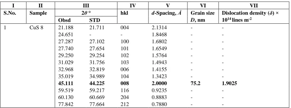
The XRD pattern in S.2(supporting information) shows step by step formation of CuS thin film particularly at 5 min (CuS 1), 10 min (CuS 2), 15 min (CuS 3), 20 min (CuS 4), 25 min (CuS 5) at pH 12 and 15 min (CuS 6) , 20 min (CuS 7), 25min (CuS 8) at pH 9. XRD analysis of as-deposited CuS thin film at 65 ⁰C showing h k l planes is given in (Fig.1), for sample CuS 8. This CuS 8 sample (pH = 10) reveals crystalline nature with the preferred orientation along (008) as observed by ICSD # 041975
card no. 78-2391, as-deposited CuS thin film samples fit into hexagonal primitive covellite CuS crystal structure. The average crystallite size and lattice constant were determined (Table 1 and Table 2) by fitting the intense diffraction peak (008) to Gaussian function and using the Debye–Scherer formula.
20 30 40 50 60 70 80
Sample CuS 8 (100)(101)
(116) (104)
(008) (004)
Figure 1. XRD analysis of as-deposited CuS thin film at 65 °C showing h k l planes
The lattice constant found to be a = 4, c = 16 and it goes with the standard value. The grain size was also estimated using the FWHM from Scherer's relationand it is of the order of 72.5 nm. Slight variation in diffraction peak width indicates strain present in the films, due to the lattice mismatch between material and substrate and other crystallographic defects that may be present in the film. The existence of extra peak in the close vicinity of (004) is either a consequence of impurity phase formation or the lattice distortion due to internal strain present in the film samples. The other parameters calculated are dislocation density, micro strain, cell volume with respect to (008) plane.
The calculations done in (Table 1 and Table 2) are done by following formulas:
Average grain size by Debye Scherer’s equation
Average strain by stokes Wilson equation:
Dislocation density (lines m-2)
d-Spacing by Bragg’s equation
2 sin (4)
n d
Lattice geometry 0.9
(1) cos
D
(2) strain 4 tan
1
(3) 2
D
2θ
⁰ I
Table 1. Showing 2θ°, hkl planes, d-spacing, grain size, and dislocation density of CuS thin film
I II III IV V VI VII
S.No. Sample 2θ ° hkl d-Spacing, Å Grain size
D, nm
Dislocation density (δ) × 1014 lines m-2
Obsd STD
1 CuS 8 21.188 21.711 004 2.1314 - -
24.651 - - 1.8468 - -
27.287 27.102 100 1.6802 - -
27.740 27.654 101 1.6549 - -
29.250 29.254 102 1.5764 - -
31.029 31.756 103 1.4943 - -
32.968 32.819 006 1.4155 - -
35.019 34.989 104 1.3423 - -
45.111 44.225 008 2.0000 75.2 1.9025
59.519 59.217 116 0.9235 - -
60.130 60.669 204 0.8883 - -
77.842 77.664 212 0.7880 - -
Table 2. Showing 2θ°, hkl planes, microstrain, cell parameters and cell volume of CuS thin film
I II III IV V VI VII
S.No. Sample 2θ° hkl Microstrain,
×10-3
Cell parameters, Å Cell Volume, Å3
Obs STD Obs STD Obs STD
1 CuS 8 45.111 44.225 008 1.246×10⁻³ a 4 16 221.69 204.15
c 3.796 16.360
a) Cell volume of hexagonal structure
b) Plane spacing hexagonal structure
AFM Studies
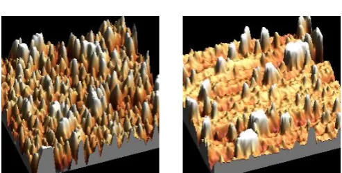
Atomic force microscopy (AFM) is an excellent tool to study morphology and texture of diverse surfaces. The knowledge of the surface topography at nanometric resolution made possible to probe thin film surfaces. The versatility of this technique allows meticulous observations and evaluations of the textural and morphological characteristics of the films, showing better facilities than other microscopic methods. AFM scanned the surface in 3D and the analysis of the images allow the determination of the average height of the particles, the root mean square roughness and the power spectra density gives the periodicity in the arrangement of particles.21 Using adequate software, it is possible to
evaluate characteristics such as roughness, porosity, average size, and particle size distribution, which influence directly the optical, mechanical, surface, magnetic and electrical properties of thin films. The (Fig. 2) corresponds to the surface morphology of our set of films, CuS 1- CuS 8.
The Atomic Force Microscopy images gave us information about the representative surface morphology and roughness for the case of the CuS. From the images we can have information that other than spherical crystal shows nanothinfilm formation; subsequently nanorods of CuS formation can be evident from cone shape, spiky structure. A 2D view of AFM picture shows that the presence of hills on the top of a homogeneous granular surface of CuS. The smaller grains are joined together to form bunches of grains present in entire surface of the films. The AFM images correlated with XRD patterns and also indicate a columnar growth of CuS films. Also some lacks and voids are observed in (Fig.2) for CuS 1- CuS 8. The nano level grains with pin holes and voids are observed in 2D image. AFM reveals the granular nature of particles and agglomeration of particles is seen from
the 3D micrographs. In (Fig 2) CuS 2, CuS 3, CuS 4, CuS
5 and CuS 7 the grains are distributed homogeneously with a pattern consistent with polycrystalline film. The optimized conditions are suitable for opto-electronic applications. The Surface roughness profile of CuS thin
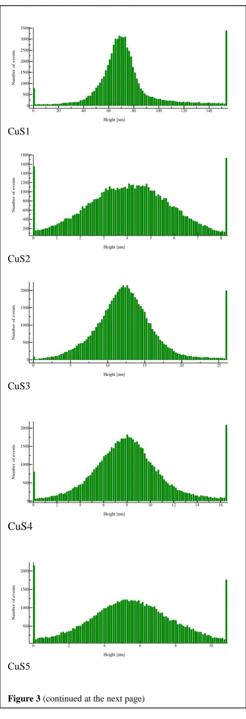
films are shown in (Fig.3) was plotted using WSxM
software and the estimated surface roughness is given in
(Table 3). The Root Mean Square (RMS) roughness
which is defined as the standard deviation of the surface height profile from the average height is the most commonly reported measurement of surface roughness.22
The RMS roughness calculates the standard deviation of the surface irregularities with respect to some mean line or curve. It is commonly used to characterize optical components, in general the lower the RMS value, the less light is scattered by an optical surface, and hence the better the surface quality.23 This parameter is used when
3 2
(5) 2
V a c
2 2
1 4 2
(6)
2 3 2 2
k l
h kh
d a c
Fig.2: AFM studies on as deposited CuS thin films at 65 °C,
showing different magnification from
CuS1-CuS8
the distribution of surface irregularities is random. Its value depends on the sampling length. The root-mean square (RMS) roughness seems to get decreased from
CuS 1(28.33 nm) to CuS 8(22.3246 nm) sample. The
maximum value of RMS is observed for CuS 6 prepared thin film and value about 36.3813 nm. The change of surface roughness is due to the crystallite size variation. This may be attributed to the selective adsorption reaction
at this concentration. The CuS 8 sample finally deposited film having low value of RMS shows that it has better surface quality. The films CuS 6 sample having high RMS value is observed to exhibit superior quality and is attributed to the selective adsorption reaction favouring stoichiometric occupancy of the metallic and non-metallic sites. From the values of surface skewness in Table 3, type of skewness is positive asymmetry for CuS 1, symmetric distribution for CuS 2, CuS 3, CuS 4, CuS 7, CuS 8, negative asymmetry for CuS 5, CuS 6 by condition S > 0 positive asymmetry, S = 0 symmetric distribution and S < 0 negative asymmetry. Similarly by values of surface kurtosis in (Table 3), type of surface kurtosis is leptokurtic distribution for CuS 1, CuS 3, CuS 8, mesokurtic distribution for CuS 4, and platykurtic distribution for CuS 2, CuS 5, CuS 6, CuS 7 by condition K > 3 leptokurtic distribution, K = 3 mesokurtic distribution, K < 3 platykurtic distribution.
Optical Studies
The optical absorption spectra of CuS thin films deposited on a glass substrate were studied at 65 ⁰C temperature in the range of wavelengths 300 – 800 nm. The variations of absorbance and transmittance with wavelength of CuS 8 sample are shown in Fig.4 and S.3
(supporting information) respectively. The films show a slight absorbance in range of 300-350 nm and an increase in transmission from 400 nm to 800 nm.
Table 3. Showing surface roughness profile of CuS thin film
140 120 100 80 60 40 20 0 3500
3000
2500
2000
1500
1000
500
0
Height [nm]
N
um
be
r
of
e
ve
nt
s
CuS1
8 7 6 5 4 3 2 1 0 1800 1600 1400 1200 1000 800 600 400 200
Height [nm]
N
um
be
r
of
e
ve
nt
s
CuS2
25 20
15 10
5 0
2000
1500
1000
500
0
Height [nm]
N
um
be
r
of
e
ve
nt
s
CuS3
16 14 12 10 8 6 4 2 0 2000
1500
1000
500
0
Height [nm]
N
um
be
r
of
e
ve
nt
s
CuS4
10 8
6 4
2 0
2000
1500
1000
500
Height [nm]
N
um
be
r
of
e
ve
nt
s
CuS5
I II III IV V VI VII
S.No. Sample
RMS(root mean square) Roughness, nm
Roughness Average, nm
Average Height, nm
Surface Skewness
Surface Kurtosis
1 CuS 1 28.3300 18.7800 75.3092 1.058 5.2473
2 CuS 2 1.8994 1.5255 4.1202 0.0141 2.6526
3 CuS 3 4.3813 3.1836 12.6631 0.7637 4.7169
4 CuS 4 3.1842 2.3761 8.1632 0.3597 3.7927
5 CuS 5 2.5392 2.0159 5.4724 -0.0325 2.7180
6 CuS 6 36.3813 28.7980 76.671 -0.0203 2.6869
7 CuS 7 1.8342 1.4504 4.1134 0.2239 2.8536
8 CuS 8 22.3246 15.5907 55.6772 0.7801 4.2120
Conclusion
Deposition of nanocrystalline CuS thin film is made feasible by an aqueous alkaline chemical bath deposition process. The film growth is found to be dependent on the pH of the reaction bath. The films are found not to be smooth and adherent to substrate at pH 12, whereas for smooth and adherent film deposition, pH 9 found to be good. HRXRD studies also confirmed crystalline hexagonal primitive nature of the film with preferred orientation along (008). AFM surface morphology studies also revealed crystalline nature of the films with randomly oriented crystallites of both irregular and spherical shapes and similar in sizes, and nanorod formation also taken place. The surface morphology of the films deposited using 0.1 M concentration for reactants, was observed quite uniform and well covered on the substrate for pH 9 than other samples. AFM image shows the thin films prepared at pH 9 are homogeneous and well covered on the substrate. These thin films consist of small grains which lead to deposition of smoother films. However, as the pH increases up to 12, the number of grains decreases and larger grain size could be obtained. Therefore, the pH plays a major role in synthesis of CuS thin film and the pH 9 is considered good under current conditions. Theoptimized conditions
are suitable for opto-electronicapplications.
Acknowledgement
We are grateful to UGC-DAE Consortium for Scientific Research INDORE-CENTRE, DAVV Campus,
Khandwa Road, Indore 452017, and India. Authors are
thankful to Prof. Ajay Gupta, for providing the experimental facilities at UGC-DAE CSR Indore. Authors are also thankful to Dr. V.R. Reddy and Mr. Anil Gome for HRXRD measurements, Dr. V. Ganesan and Mr. Mohan Gangarade extending the AFM measurements.
References
1Ghosh, C., Verma, B. P., Thin Solid Films., 1979, 60, 61. 2Nayak, B. B., Acharya, H. N., Chaudhari, T. K., Mitra, G.
B., Thin Solid Films., 1982, 92, 309.
3Pavaskar, N. R., Menzes, C. A., Sinha, A. P. B., J.
Electrochem. Soc., 1977, 124, 743.
4Pawar, S. H., Tamhankar, S., Bhosle, P. N., and Uplane,
M. D., Thin Solid Films.,1983, 110, 165.
120 100 80 60 40 20 0 1800 1600 1400 1200 1000 800 600 400 200
Height [nm]
N
um
be
r
of
e
ve
nt
s
CuS6
8 7 6 5 4 3 2 1 0 2000
1500
1000
500
0
Height [nm]
N
um
be
r
of
e
ve
nt
s
CuS7
100 80
60 40 20
0 3000
2500
2000
1500
1000
500
0
Height [nm]
N
um
be
r
of
e
ve
nt
s
CuS8
Figure 3. Surface roughness profile spectra of CuS thin film deposited at various time interval CuS1- CuS8.
5Pawar, S.H., Tamhankar,S., Bhosle,P.N., and
Uplane,M.D., Ind. J. Pure Appl. Phys., 1983, 2, 665.
6Pawar, S. H., Bhosale, P. N., Mater. Chem. Phys., 1984,
11, 461.
7Partain, L. D., Mcleod, P. S., Duisman, J. A., Peterson, T.
M., Sawyer, D. E., Dean, C. S., J. Appl. Phys.,
1983, 54, 6708.
8 Marco, R. De., Mattrall, R., Liesegang, J., Nyberg, G.,
Hamilton, I., Anal. Chem., 1992, 64, 594.
9Mattox, G. M., and Sowel, R. R., J. Vac. Sci. Technol., 1974, 1, 793.
10Agnihotri, O. P., and Gupta, B. K., Solar selective
surfaces, Wiley, New York, 1981.
11Rothwarf, A., Meakin, J. D., and Bamett, A. M.,
Polycrystalline and amorphous thin films and
devices, Academic Press, New York, 1980.
12Savelli, M., and Bougnot, J., Topics in applied physics,
Ed.: Seraphim,B. O., Springer, Berlin, 1979.
13Grozdanov, I., Barlingay, C. K., Dey, S. K., Mater. Lett., 1995, 23, 181.
14Pathan, H. M., and Lokhande, C. D., Bull. Mater. Sci: 2004, 27(2), 85–111.
15Evans, H. T., Am. Mineral., 1981, 66, 807. 16Goble, R. J., Can. Minerol., 1985, 23, 61.
17Wyckoff, R. W. G., Crystal Structures, New York:
Interscience, 1965.
18 Evans, H.T., Am. Mineral., 1981, 66, 807.
19Popovici, I., Isac, L., Duta, A., Bull. Transilv. Univ., 2009, 2, 5.
20Nducwe, I. C., Solar Energy Mater. Solar Cells, 1996,
40, 123.
21Howland, Rebeca., and Benater, Lisa., A practical guide
to scanning probe Microscopy, 1997, 1.
22Jiang, T., Hall, N., Ho, A., and Morin, S., Thin Solid
Films, 2005, 417, 76.
23Bhushan, Bharat., Fuchs, Harold., Hosaka, Sumio.,
Applied scanning probe methods, Springer,
Berlin-Heidelberg-New York , 2004, 292.
24Gosavi, S. R., Deshpande, N. G., Gudage, Y. G.,
and Sharma, Ramphal., J. Alloys Compds., 2008,
448, 344.
25Singh, R. S., Bhushan, S., Singh, A. K., Deo, S. R., Dig.
J. Nanomater. Biostruct., 2011, 6, 403.
26 Singh, Ajaya Kumar., Thool, Gautam Sheel., Deo,
Soumya R., Singh, R. S., Gupta, Ashish., Res. Chem.
Intermed., DOI 10.1007/s11164-012-0524-y.
27Singh, R.S., Bhushan,S., Singh,A.K., Chalc. Lett., 2010,
7, 375.
28Singh,R.S., Bhushan,S., Singh,A.K., J Ovonic. Res., 2010, 6, 211.
29Pejova, B., Grozdanov, I., J. Solid State Chem., 2001, 158, 49.
30Mamun,Al., Islam, A. B. M. O., and Bhuiyan, A. H., J.
Mater. Sci. Mater. Electr., 2005, 16, 263.
31Lakshmi, M., Bindu, K., Bini, S., Vijayakumar,
K.P., Kartha, S., Abe, T., Kashiwaba, Y., Thin
Solid Films, 2000, 370, 89.
32Nair, P. K., Cardoso, J., Daza, O. Gomez., Nair, M.
T. S., Thin Solid Films, 2001, 401, 243.
33Nien, Y. T., Chen, I. G., J. Alloys Compds., 2008,
471, 553.
34Sagade, A. A., Sharma, R., Sensors Actuators, 2008,
B133, 135.
35Bagul, S.V., Chavhan, S.D., Sharma, R., J. Phys.
Chem. Solids, 2007, 68, 1623.
36Pramanik, P., Akhter, M.A., Basu, P.K.,J. Mater. Sci.
Lett., 1987, 6, 1277.