ISSN 2319-7617 (Online)
(An International Research Journal), IF = 4.715,www.physics-journal.org
Study on the Photoluminescence
Usha Shukla and Samreen Bari
Amity University Lucknow email:[email protected]
(Received on: May 2, 2018)
ABSTRACT
Photoluminescence (PL) is the emission of light from any matter after the absorption of photon because it is initiated by photo excitation. In photoluminescence it is observed that at certain energy it can be viewed as indication that excitation population an excited state associated with its transition energy. Photoluminescence properties are also extremely sensitive to the dielectric environment and to the internal electric fields which impose further degrees of complexity. Photoluminescence study gives a number of interesting intrinsic effects in quantum wells, like the excitation binding energy increase due to charge carrier localization, the homogeneous broadening of the excitation recombination line, the carrier–carrier interaction etc. The analysis of the radiative recombination spectra of nanostructures can help in the characterization of the structure, providing information on the interface morphology and on the quality of the materials. This paper reports mechanisms, importance, applications and experimental techaniques for photoluminescence.
Keywords: Photoluminescence, carriers interaction, quantum well and photo excitation.
I. INTRODUCTION
Cold emission of light is called luminescence. When the energy is absorbed by substance in any form, a fraction of absorbed energy may be re-emitted in the form of electromagnetic radiation. It possess two processes first the excitation of the electronic system of the substance and the second subsequent emission of photon. This phenomenon is called luminescence. It is also named after the excitation energy.
A. Types of luminescence
a. Photoluminescence: It is emission of light from any matter after the absorption of photon. b. Electroluminescence: It occurs upon the application of an alternating electric field to the
c. Chemiluminescence: It is the result of chemical reaction in which emission of light take place. It is different from phosphorescence and fluorescence in which the excited state is the product of chemical reactions instead of the absorption of photon.
d. Radioluminescence: when bombardment with ionizing radiation take place its produce the light in the material. It is used as low light source.
e. Lyoluminescence: when solid is dissolving into a liquid solvent emission of light is take place then it is called lyoluminescence. It is the form of chemiluminescence.
f. Thermoluminescence: The process in which light is emitted by minerals while it is heated.
B. Photoluminescence
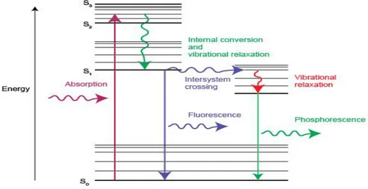
When a light emitted from any matters after the absorption of photon it is called Photoluminescence because it is initiated by photo excitation. In photoluminescence it is observed that at certain energy it can be viewed as indication that excitation population an excited state associated with its transition energy. When a substance is illuminated by laser both photoluminescence and Raman scattering can occur. The latter can be stronger than the former and it can prevent Raman analysis. When the photoluminescence of a trace is optimized at a specific excitation wavelength, its emitted light will be captured within a specific bandwidth (by either a band-pass filter or selective goggles). These filters lower the intensity of the response, which makes it mandatory to work in full darkness with this technique. Working in the dark with yellow or orange goggles, the CSI should begin to screen with a large excitation blue band (in an interval covering 450 nm), labeled “CS Blue,” or a low-pass filter (LPF), selecting wavelengths under a specific threshold4. Photoluminescence comprises both
phosphorescence and fluorescence process the amount and type of process depends by the material you are studying and the wavelength of laser which we are using3. Figure 1 shows
the absorption of light.
C. Forms of Photoluminescence
a. Resonant radiation:- In this, a photon is absorbed and an equivalent photon is immediately emitted through which no significant internal energy transition of the chemical substrate between emission & absorption are involved6.
b. Fluorescence:- In this process, when the substance undergoes internal energy transition before relaxing its ground state by emitting photon, some of the absorbed energy is dissipated so the emitted photons are of lower energy than absorbed6.
c. Phosphorescence:- In this, absorbed energy undergoes intersystem crossing into a state with a different spin multiplicity and its lifetime is much longer than the fluorescence. Hence, it is rarer than fluorescence6.
II. MECHANISM OF PHOTOLUMINESCENCE
Semiconductor is excited with a light source that provides photon with energy larger than the band gap energy. Once the photons are absorbed then holes and electrons are formed with finite momentum in the valence band and conduction respectively. Excitation then undergoes energy and momentum relaxation towards the band gap minimum. Finally, the electrons recombine with holes under emission of photons. Photoluminescence properties are also extremely sensitive to the dielectric environment and to the internal electric fields which impose further degrees of complexity2.
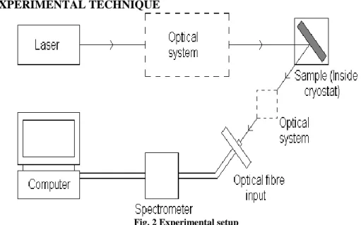
III. EXPERIMENTAL TECHNIQUE
Fig. 2 Experimental setup
beam propagate in different direction5. A filter maybe placed in front of the fiber input which
remove any incident laser light and the emitted light is directed to the fiber optics and then to the spectrometers. Inside the spectrometer a diffraction grating of different wavelength in different directions towards an array of photo detector that measure the intensity of each wavelength component and the computer shows the information which can display a photoluminescence spectrum which indicates the intensities of light at different wavelength enter into the detector.
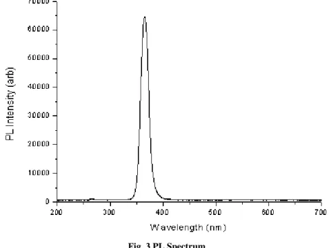
IV. PL SPECTRUM
The example of PL spectrum is shown in Fig. 3 which is experimentally obtained. The wavelength at which peak intensity occurs is 367nm, corresponds to a photon energy of 3.4eV 1.
Fig. 3 PL Spectrum
V. IMPORTANCE OF PHOTOLUMINESCENCE
VI. APPLICATIONS
a. Band gap determination:- The energy difference between valence bands and conduction band is called the band gap. Spectrum distribution of photoluminescence determines the electronic band gap non-destructively. This gifts means to quantify the elemental composition of semi conductor compound and is an important material of sole cell device efficiency.
b. Impurity levels and defects detection:- Radiative transitions involve localized defect levels in semiconductor. Specific defects can be identifying by the photoluminescence energy associated with these levels. Photoluminescence spectrum at low temperature often reveals spectral peaks associated with impurities contained within the host material and the Fourier transform of photoluminescence micro spectroscopy, provides the potential to identify extremely low concentration of unintentional and intentional impurities which can strongly affected the device performance and the material quality.
c. Surface structure and excited state:- The most used methods named as XRD , IR and raman spectroscopy are non sensitive in support of oxide catalysts with concentrations of low metal oxide. Pholuminescence , however , is very sensitive to adsorbed species of semiconductor’s surface effects and this is the reason particles are used as a probe of electron-hole surface processes.
d. Recombination Mechanism:- process.Coming back to its equilibirium is known as ‘recombination’ which consists both radiate and non-radiate processes.The amount of photoluminescence which is emitted from a material depends upon the relative quantity of non-radiative and radiative recombination rates.Non-radiative rates are related to the impurities and quantity of photoluminescence and its relation to the level of photo-excitation and temperature depends upon the dominant recombination.
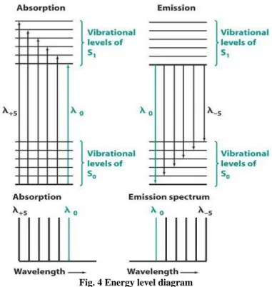
VII. RELATION BETWEEN ABSORPTION ANDEMISSION SPECTRA
Absorption comes at higher energy than fluorescence and phosphorescence. In absorption λₒ wavelength correspond to a transition to the lowest vibrational level of S1 from
the ground vibrational level of Sₒ. After absorption S1 molecule relax back to the lowest
vibrational level of S1 prior to emitting any radiation. The highest energy transition comes at
λₒ wavelength with a series of peak following at longer wavelength. If the transition probabilities are similar and if the spacing between vibrational levels is roughly equal then the absorption and emission spectra have an appropriate mirror image relation. The λₒ transitions do not exactly overlap a molecule absorbing radiation in its electronic ground state Sₒ. When the radiation is absorbed the excited S1 molecules still possess its Sₒ geometry and salvation.
After excitation their geometry and salvation change to their most favorable value for S1 state.
When the S1 fluoresces molecule written to the Sₒ state with S1 geometry and salvation and
Fig. 4 Energy level diagram
VIII. TEMPERATURE DEPENDENCE PHOTOLUMINESCENCE
Photoluminescence intensity of nano-phosphors decreases with the temperature and tends to disappear beyond a particular temperature .The critical temperatures beyond which PL disappear in the nano-phosphors are 228oC,251oC and 278oC for CdS: Cu nanophosphors
at 150 oC,100oC and room temperature. The decrease of PL intensity with temperature is due to the increase in probability of non radioactive transition. In the PL process the valence electrons are more responsible for the emission7.
IX. CONCLUSIONS
We have studied the Photoluminescence and its forms, and also studied the relation between absorption and emission spectra and it seems they are roughly mirror image of each other and also their applications
REFERENCES
2. M. Kira, F. Jahnke, S.W. Koch, Quantum Theory of Secondary Emission in Optically Excited Semiconductor Quantum Wells, Phys. Rev. Lett. 82, 3544–3547 (1999).
doi:10.1103/PhysRevLett.82.3544.
3. Renishaw, Photoluminescence explained, Renishaw. 1–4 (2015).
http://www.renishaw.com/media/img/en/50e033cc197a416db28909dc584e38a1.jpg (accessed April 19, 2018).
4. S. Sanguinetti, M. Guzzi, M. Gurioli, Accessing structural and electronic properties of semiconductor nanostructures via photoluminescence, in: Charact. Semicond. Heterostruct. Nanostructures, Elsevier, pp. 175–208 (2008).
doi:10.1016/B978-0-444-53099-8.00006-3.
5. M.C. Scharber, D. Mühlbacher, M. Koppe, P. Denk, C. Waldauf, A.J. Heeger, C.J. Brabec, Design Rules for Donors in Bulk-Heterojunction Solar Cells—Towards 10 % Energy-Conversion Efficiency, Adv. Mater. 18, 789–794 (2006). doi:10.1002/adma.200501717. 6. A.M. White, E.W. Williams, P. Porteous, C. Hilsum, Applications of photoluminescence
excitation spectroscopy to the study of indium gallium phosphide alloys, J. Phys. D. Appl. Phys. 3, 312 (1970). doi:10.1088/0022-3727/3/9/312.