Processor-based Benchmarks on FPGA Devices
by
Jiunn-Tyng, Kao
A Doctoral Thesis submitted in partial fulfilment of the requirement for Master of Philosophy of
Loughborough University
January 2014
_________________________________________________
Abstract
The computing system on SoCs is being long-term research since the FPGA technology has emerged due to its personality of re-programmable fabric, reconfigurable computing, and fast development time to market. During the last decade, uni-processor in a SoC is no longer to deal with the high growing market for complex applications such as Mobile Phones’ audio and video encoding, image and network processing. Due to the number of transistors on a silicon wafer is increasing, the recent FPGAs or embedded systems are advancing toward multi-processor-based design to meet tremendous performance and benefit this kind of systems are possible. Therefore, is an upcoming age of the MPSoC. In addition, most of the embedded processors are soft-cores, because they are flexible and reconfigurable for specific software functions and easy to build homogenous multi-processor systems for parallel programming. Moreover, behavioural synthesis tools are becoming a lot more powerful and enable to create datapath of logic units from high-level algorithms such as C to HDL and available for partitioning a HW/SW concurrent methodology.
A range of embedded processors is able to implement on a FPGA-based prototyping to integrate the CPUs on a programmable device. This research is, firstly represent different types of computer architectures in modern embedded processors that are followed in different type of software applications (eg. Multi-threading Operations or Complex Functions) on FPGA-based SoCs; and secondly investigate their capability by executing a wide-range of multimedia software codes (Integer-algometric only) in different models of the processor-systems (uni-processor or multi-processor or Co-design), and finally compare those results in terms of the benchmarks and resource utilizations within FPGAs. All the examined programs were written in standard C and executed in a variety numbers of soft-core processors or hardware units to obtain the execution times. However, the number of processors and their customizable configuration or hardware datapath being generated are limited by a target FPGA resource, and designers need to understand the FPGA-based tradeoffs that have been considered - Speed versus Area.
For this experimental purpose, I defined benchmarks into DLP / HLS catalogues, which are "data" and "function" intensive respectively. The programs of DLP will be executed in LEON3 MP and LE1 CMP multi-processor systems and the programs of HLS in the LegUp Co-design system on target FPGAs. In preliminary, the performance of the soft-core processors will be examined by executing all the benchmarks. The whole story of this thesis work centres on the issue of the execute times or the speed-up and area breakdown on FPGA devices in terms of different programs.
Keywords:
Soft-core, Multi-core, Co-design, Electronic-system-level, High-level-synthsis, Thread-level-parallelism, Data-level-parallelism, Symmetric-multi-processor, RISC, VLIW, LEON3
_________________________________________________
Acknowledgements
This research was supported by the research group of Electronic Systems Design, School of Electronic and Electrical Engineering, Loughborough University, UK. I first would like to thank my supervisor and this research leader, Dr Vassilios Chouliaras. Secondly, I would like to thank my lab colleagues; David Stevens for the rearrange of Lempel-Ziv-Welch compression C code. He is a master of C programming language and Linux Ubuntu operating system and always opens for an answer; and Mark Milward for simulations of the LE1 CMP benchmarks. He is an expert in FPGA and SoC design. His help and advice have greatly helped my experimental analysis and philosophy.
_________________________________________________
TABLE OF CONTENTS
Abstract……….……….………...…………..……...…..2 Acknowledgments……….……….………...…………..……...….3 Table of Contents……….……….………...…………..……...….4 Table of Abbreviations……….……….………...…………..……...….8 List of Figures……….……….………...…………..……...…13 List of Tables……….……….………...…………..……...…16 1 Introduction……….……….………...…………..……...…17 1.1 Motivation……….………...………...……..171.2 Aims and Objectives of this Research…... 18
1.3 Objectives of the Research and Goals…...19
1.4 Organization of the Thesis…...22
2 Background Research and State of the Art …...24
2.1 Introduction………...……...………..24
2.2 Types of Parallelism.………...…2 7 2.2.1 Instruction-Level-Parallelism (ILP)…... 27
2.2.2 Data-Level-Parallelism (DLP)………...………28
2.2.3 Thread-Level-Parallelism (TLP)………...……….28
2.3 State-of-the-Art in Electronic-System-Level (ESL) Design ………....29
2.3.1 Hardware/Software (HW/SW) Co-designs…...30
2.4 FPGA Devices Overview………..…....31
2.4.1 FPGA Fundamental Structures...31
2.4.2 Advanced FPGA Features………...33
2.5 Embedded Processors on FPGAs………..…...34
2.5.1 Hard and Soft Processors…... 36
_________________________________________________
2.6 Summary………..………...………38
3 Background of Methodologies and Implementations...………40
3.1 Introduction…... ...40
3.2 Implementations of Data-Level-Parallelism (DLP)...…...40
3.3 Implementations of High-Level-Synthesis (HLS)………..…...41
3.4 Design-Space-Exploration (DSE) on FPGA-Based...44
3.4.1 Xilinx and Altera Resource Usage Conversion…...44
3.4.2 DSE of Multi-core Processor System…... 46
3.4.3 DSE of Co-design System...46
3.5 Summary………...47
4 Evaluation in Single-core of Soft Embedded Processors…...48
4.1 Introduction…... 48
4.2 Background of LEON3, LE1, and Tiger-MIPS Processors…...…………48
4.2.1 The LEON3 Processor………...…….49
4.2.2 The LE1 Processor………...………52
4.2.3 The Tiger-MIPS Processor…...54
4.3 The Software (SW) Flow…... ..55
4.3.1 Experimental Implementations... ..55
4.4 Benchmark Collections…... .55
4.4.1 Data-intensive Programs………...……….56
4.4.2 Function-intensive Programs…...56
4.4.3 Other Programs…... ...57
4.5 Evaluations of Speed&Area in Single-core of Soft-processors…...58
4.6 Summary…... ...63
5 Evaluation in Data-level-parallelism of LEON3 MP and LE1 CMP on FPGA-based SMPs………...…...………...………64
_________________________________________________
5.1 Introduction…... ...64
5.2 LEON3 and LE1 Multi-core Processor Methods…...64
5.2.1 RISC vs VLIW…... ...65
5.2.2 Symmetric-Multi-Processors (SMPs) with Data-Level-Parallelism (DLP)…...66
5.2.3 LEON3 MP and IPs Configuration…...67
5.2.4 LE1 CMP and Configurability... .68
5.3 The Parallel-SW Flow... ...69
5.3.1 LEON3 CPUs Identification…...7 0 5.3.2 LE1 Contexts Indentify…... 70
5.3.3 Structures LEON3 MP & LE1 CMP and System Clock on the FPGA...…...70
5.4 Benchmarks of Data-Level-Parallelism (DLP)…...72
5.4.1 Convolution-Matrix (CM)…... ..72
5.4.2 Lempel-Ziv-Welch (LZW)…... 73
5.5 Evaluation and Comparison of LEON3MP and LE1 CMP…...75
5.5.1 Analysis of Performance and Area...75
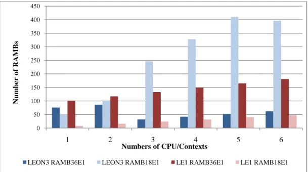
5.5.2 Distribution of Block RAMs on the FPGA...77
5.5.3 Synchronized Confliction and Speed&Area Tradeoffs...…...78
5.6 Summary………...………...……80
6 Evaluation in High-level-synthesis of LegUp Co-design System on FPGA-based Processor...8 1 6.1 Introduction………...………...………81
6.2 LegUp Co-design System and Program Profiling...81
6.2.1 The Call-graph Profiler (Kcachegrind)………….………...…….82
6.3 LegUp Architecture and Designed Flows……….………...….83
6.3.1 The Hardware (HW) Flow...84
_________________________________________________
6.4 Benchmarks of High-Level-Synthesis (HLS)…...87
6.4.1 Microprocessor.………...…87
6.4.2 Double Precision Floating-point Arithmetic...87
6.4.3 Media Processing.………...…...…88
6.4.4 Security.………...……89
6.5 Experimental Methodology and Results…... 89
6.5.1 Analysis of Profiling Data...90
6.5.2 Analysis of Speed and Resource Utilization...………...…………91
6.5.3 Distribution of DSPs and Block RAMs on FPGAs...91
6.5.4 Speed&Area Tradeoffs in LegUp System on FPGAs...93
6.6 Summary………...96
7 Overall Outline and Conclusion... ...97
7.1 Conclusion of LEON3, LE1, and Tiger-MIPS Soft-cores...97
7.2 Conclusion of DLP in LEON3 MP and LE1 CMP...98
7.3 Conclusion of HLS in LegUp Co-designs...99
References…... ...100
Appendix…... ...108
Appendix I Benchmark Collections - SW Flow...108
I.1 SW flow in LEON3, LE1, and Tiger-MIPS Processors…...108
Appendix II DLP Benchmarks - Parallel-SW Flow…...109
II.1 Parallel-SW flow in LEON3 MP and LE1 CMP……….…109
Appendix III HLS Benchmarks - HW, Hybrids, and SW Flows………..…...…111
III.1 Called-graphs of Profiling for Benchmarks by Kcachegrind…...111
III.2 Top Most Called-functions for Benchmarks...…...120
_________________________________________________
TABLE OF ABBREVIATIONS
Abbreviation Expansion
ADD Addition
ADPCM Adaptive Differential Pulse Code Modulation
AES Advanced Encryption Standard
AHB Advanced High-performance Bus
ALAP As Late As Possible
ALM Adaptive Logic Module
ALU Arithmetic Logic Unit
ALUT Adaptive LUT
AMBA Advanced Microcontroller Bus Architecture
ANSI American National Standards Institute
APB Advanced Peripheral Bus
ASAP As Soon As Possible
ASIC Application Specific Integrated Circuit
BCC Bare-C Cross-compiler system
BITOP Bitwise Operation
c-step control step
CAD Computer Aided Design
CLB Configurable Logic Block
CM Convolution Matrix
CM60x60 Convolution Matrix with 60x60 output data
CMOS Complementary Metal Oxide Semiconductor
CMP Chip Multi Processor
CPU Central Processing Unit
CPUID CPU Identification
D-cache Data Cache
D-RAM Data RAM
DCT Discrete Cosine Transform
DDR SDRAM Double Data Rate SDRAM
DE2 Development and Education 2
_________________________________________________
DFADD Double Precision Floating-Point Addition
DFDIV Double-precision Floating-Point Division
DFG Data Flow Graph
DFMUL Double-precision Floating-Point Multiplication
DFSIN Double-Precision Floating-Point Numbers of Sine function
DFT Discrete Fourier Transform
DIV Divider
DLL Delay Locked Loop
DLP Data Level Parallelism
DSE Design Space Exploration
DSP Digital Signal Processing
DSU Debug Support Unit
EDA Electronic Design Automation
ESL Electronic System Level
FF Flip-Flop
FFT Fast Fourier Transform
FIFO First In First Out
FIR Finite Impulse Response
Fmax Maximum Frequency
FPGA Field Programmable Gate Array
FPU Floating Point Unit
FSL Fast Simplex Link
FU Functional Unit
GB Gigabyte
GCC GNU Compiler Collection
GDS Global Positioning System
GPR General Purpose Register
GPS Global Positioning System
GRLIB Gaisler Research Library
GSM Global System for Mobile
GUI Graphical User Interface
HDL Hardware-Description-Language
HI Multiply and Divide Register Higher Result
HLS Electronic System Level
_________________________________________________
HW Hardware
I-cache Instruction Cache
I-RAM Instruction RAM
IALU Integer-ALU
IC Integrated Circuit
IFE Instruction Fetch Engine
ILP Instruction Level Parallelism
IMULT Integer-MULT
IP Intellectual Property
IR Integer Register
IRQ Interrupt Controller Register
IU Integer Unit
JAL Jump and Link
JPEG Joint Photographic Experts Group
JTAG Joint Test Action Group
KB Kilobyte
LAB Logic Array Block
LAT Latency
LC Logic Cell
LE Logic Element
LLVM Low Level Virtual Machine
LMB Local Memory Bus
LO Multiply and Divide Register Lower Result
LP Linear Program
LPC Linear Predictive Coding
LRR Least Recently Replaced
LRU Least Recently Used
LSU Load Store Unit
LUT Look Up Table
LZW Lempel Ziv Welch
LZW45K Lempel Ziv Welch with size of 45KB input data
MAC Media Access Control
MB Megabyte
MHz Megahertz
_________________________________________________
MIMD Multiple Instruction Multiple Data
MIPS Microprocessor without Interlocked Pipeline Stages
MISD Multiple Instruction Single Data
MMU Memory Management Unit
MP Multi Processor
MP3 MPEG-1 Audio Layer-3
MPEG Moving Picture Experts Group
MPSoC Multi-processor System on Chip
ms millisecond
MUL Multiplier
MUX Multiplexer
NISC No Instruction Set Computer
NOP No Operation
NRE Non Recurring Engineering
ns nanosecond
OPB On-chip Peripheral Bus
PAR Place and Route
PB Petabyte
PC Program Counter
PDA Personal Digital Assistant
PDF Portable Document Format
PIC Peripheral Interface Controller
PLB Processor Local Bus
PLL Phase Locked Loop
PROC Processor
ps picosecond
RAM Random Access Memory
RAMB RAM Block
RC Resource Constraint
REG Register
REM Reminder
RISC Reduced Instruction Set Computing
RTL Register Transfer Level
SDC System of Difference Constraint
_________________________________________________
SHA Secure Hash Algorithm
SHARC Super Harvard Architecture Single Chip Computer
SIMD Single Instruction Multiple Data
SISD Single Instruction Single Data
SMP Symmetric Multi-Processor
SoC System on a Chip
SOPC System on a Programmable Chip
SPARC Scalable Processor Architecture
SPMD Single Program Multiple Data
SRA Square Root Approximate
SRAM Static Random Access Memory
SUB Subtraction
SVT Single Vector Trapping
SW Software
TB Terabyte
TC Timing Constraint
TLP Thread Level Parallelism
UART Universal Asynchronous Receiver/Transmitter
UMA Uniform Memory Access
VCO Voltage Controlled Oscillator
VEX VLIW Example
VHDL VHSIC (Very-High-Speed-IC) HDL
VLIW Very Long Instruction Word
VLSI Very Large Scale Integration
XML Extensible Markup Language
µC Microcontroller
µP Microprocessor
µs microsecond
_________________________________________________
LIST OF FIGURES
Figure 1.1: The fundamental design-flow of this thesis work...…21
Figure 2.1: ASIC&FPGA devices Design flows…...26
Figure 2.2: A five-stage instruction pipeline…...27
Figure 2.3: Data-parallelism of SIMD and SPMD…...28
Figure 2.4: Task-parallelism of MIMD…... ..29
Figure 2.5: The ESL design flow and abstraction levels...29
Figure 2.6: The HW/SW Co-design system...3 0 Figure 2.7: FPGA fundamental structures…... 32
Figure 2.8: FPGA advanced structures…... 33
Figure 2.9: The routing delays and maximum frequency within FPGAs...34
Figure 2.10: Embedded processor-systems…... ..35
Figure 2.11: The structure of shared / distributed memory of the multi-core processor systems…...38
Figure 2.12: The time-line of the computer technology…...39
Figure 3.1:
Pseudo codes for an 3-core of
SPMD multi-processor system …...41Figure 3.2: The HLS design flow... .42
Figure 3.3: ASAP and ALAP scheduling...43
Figure 3.4: A Virtex-5 LUT-FF Pairs...44
Figure 3.5: A Stratix III ALMs...45
Figure 4.1: LEON3 processor core block diagram...49
Figure 4.2: LEON3 CPU core IU datapath...51
Figure 4.3: IALU/IMULT and IALU LAT/IMULT LAT for the LE1 core...52
Figure 4.4: LE1 CPU core schematic... 53
Figure 4.5: MIPS CPU core schematic…... 54
_________________________________________________
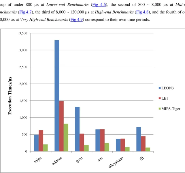
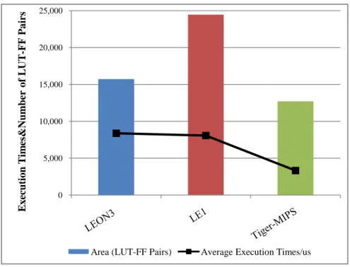
Figure 4.7: Comparison in execution times at Mid-end Benchmarks…...59
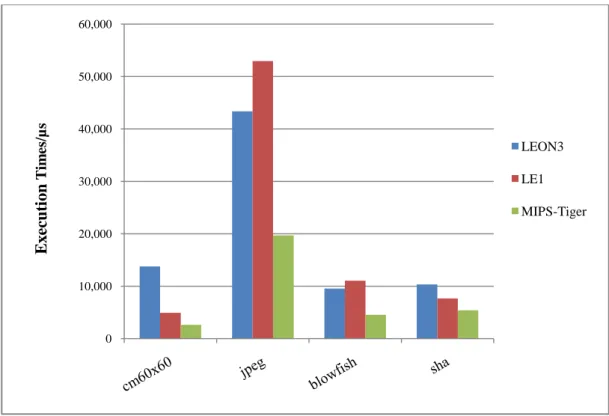
Figure 4.8: Comparison in execution times at High-end Benchmarks…...60
Figure 4.9: Comparison in execution times at Very High-end Benchmarks………...….……60
Figure 4.10: The speed and area results of LEON3&LE1&MIPS SW flow...…61
Figure 5.1: Example of RISC and VLIW instructions…...65
Figure 5.2: SMPs with DLP…... ..66
Figure 5.3: LEON3 multi-core with GRLIB IP for the SoC………...………67
Figure 5.4: Two-way multiprocessors consisting of two instances of a 4-wide, single-cluster LE1 core, the common data memory and the thread control unit…...69
Figure 5.5: LEON configuration register (%ASR17)…...70
Figure 5.6: LEON3 MP blocks diagram...71
Figure 5.7: LE1 CMP blocks diagram...71
Figure 5.8: An example of convolution matrix...72
Figure 5.9: Example of C code that an MxM input through the NxN kernel of the CM ...73
Figure 5.10: Example of C code which splits global input array over each active CPU for the LZW...74
Figure 5.11: Speed-up results of CM60x60...……...75
Figure 5.12: Speed-up results of LZW45K...….……...76
Figure 5.13: The overall performance and area results in LEON3 MP and LE1 CMP…...76
Figure 5.14: The total number of block RAMs in LEON3 MP and LE1 CMP…...78
Figure 5.15: LEON3 MP & LE1 CMP Program speed-up vs Area cost...…79
Figure 5.16: LEON3 MP & LE1 CMP Speed&Area Efficiency…...80
Figure 6.1: LegUp's FPGA target system...…82
Figure 6.2: Fragment of the call-graph.………...83
Figure 6.3: The signal port of LegUp in Verilog hardware…...84
Figure 6.4: LegUp HW/SW Co-design flows...86
_________________________________________________
Figure 6.6: Embedded multiplier 9x9-bit elements distribution. …..……...92
Figure 6.7: Total memory bits distribution…...93
Figure 6.8: The overall performance and area results of LegUp...…94
Figure 6.9: The percentage of Speed and Area tradeoffs distribution…...95
Figure 6.10: The LegUp area and speed efficiency…...95
Figure III.1: The called-graphs DFADD...111
Figure III.2: The called-graphs DFDIV...………...……….112
Figure III.3: The called-graphs DFMUL...………...….112
Figure III.4: The called-graphs DFSIN...113
Figure III.5: The called-graphs ADPCM...………...……….113
Figure III.6: The called-graphs GSM...………...………….114
Figure III.7: The called-graphs JPEG...………...……….115
Figure III.8: The called-graphs MOTION...116
Figure III.9: The called-graphs AES...116
Figure III.10: The called-graphs BLOWFISH...………...……….117
Figure III.11: The called-graphs SHA...………...…….117
Figure III.12: The called-graphs CM60x60...…...118
Figure III.13: The called-graphs LZW45K...………...….119
Figure III.A: The percentage distributions of algorithmic types in HLS benchmarks...121
Figure III.B: The percentage distributions of C control flows in HLS benchmarks...122
_________________________________________________
LIST OF TABLES
Table 2.1: Flynn’s Taxonomy.………..………...27
Table 2.2: Embedded hard-cores on FPGAs…...36
Table 2.3: Embedded soft-cores on FPGAs……….………...……36
Table 4.1: Outline of the DLP benchmark suits………56
Table 4.2: Outline of the CHStone HLS benchmark suits………56
Table 4.3: Outline of the other benchmarks………..57
Table 4.4: The Speed&Area Efficiency of LEON3&LE1&MIPS SW flow…...62
Table II.A: Benchmarks of LEON3, LE1, and Tiger-MIPS single-cores…...108
Table 5.1: LEON3 blocks configurability…... 67
Table 5.2: LE1 microarchitectural configurability………...…….68
Table II.A: LEON3 MPs and LE1 CMPs simulated execution cycles and times (at 60MHZ and 50MHZ)...109
Table II.B: LEON3 MPs and LE1 CMPs RAMS & DSPS breakdown on XILINX VIRTEX 6 ML605 FPGA... ...109
Table II.C: LEON3 MPs and LE1 CMPs total area and RAMBs breakdown on XILINX VIRTEX 6 ML605 FPGA... ...110
Table II.D: The results of speed-up versus area cost and Speed&Area Efficiency of LEON3&LE1 SMP... ...110
Table III.A: The top-four function-called in HLS benchmarks……….………..120
Table III.B: Characterizations of HLS programs... …121
Table III.C: Control flows and test-data length of HLS benchmarks...122
Table III.D: Synthesis results for HLS benchmarks on ALTERA CYCLONE II FPGAs...123
_________________________________________________
Chapter 1
Introduction
1.1
Motivation
In historical computing, the computer processor was based on vacuum tubes and started the design of stored-program (Memory-Control-FUs) to form the fundamental of computer architectures known as von Neumann (1947) [1]. The vacuum tube was replaced by much smaller and reliable transistor in the 1950s. By the 1960s, electronic processing elements began to appear based on semiconductor devices as such many transistors in a chip to form an Integrated-Circuit (IC) and thus led to the generation of the microprocessor [2]. In accordance with Moore’s Law, the number of transistors on the same chip area nearly doubles every two years [3]. Following this trend for half a century, the silicon chips have become inexpensively and a lot more complicated designing and very elated computing problems can ever be solved. Over the decades, semiconductor devices are able to accommodate the whole system (CPUs, system-bus, peripherals and internal memory) to form an embedded system, known as System-on-a-Chip (SoC). SoCs are widely used in portable devices such as PDAs, digital cameras, GPS units, MP3 players, and smart phones; larger systems such as air traffic control and missile systems [4]. Embedded processors are CPUs typically used in an embedded system. These processors are usually smaller silicon space compared, sustain lower performance, and need much less power compared to the server or desktop CPUs. Smart phones are the perfect example of an embedded system. The embedded processor is typically as an Application-Specific-Integrated-Circuit (ASIC) hard-core which built into a "floorplan" of a fixed IC or a soft-core that described by the Hardware-Description-Languages (HDLs) for a customized configuration then synthesize into a programmable fabric logic such as Field-Programmable-Gate-Array (FPGA) devices. During the last decade, multi-processor systems became available in computers and in Multi-Processor System-on-Chip (MPSoC) devices to achieve higher computing performance; and they continue to grow in further on the market [5]. At the present time, electronic products have become much more competitive and the product life cycle much shorter [6]; therefore engineers attempt to search a cheaper, easier and faster way to develop new chips. Reusable designs such as Intellectual-Property (IP) cores are instrumental when designing a new chip. While the post-fabrication of the chips has been greatly improved, the numbers of the transistors that can be fitted in the same area on a die chip are increased. In addition, the overall energy consumption of the chips has been reduced due to the dynamic power decrease when transistor becomes smaller and leakage current problem has also been solved by Triple-oxide approach [7, 8]. However, Moore’s Law will not be sustained forever as physical limitations cause problems such as heat dissipation. Moreover, it is expensive to design and fabricate a much more powerful processor on a single chip. Other factors such as, the
_________________________________________________
clock rates of embedded CPUs are increased slowly up to Gigahertz and now parallelism in multiple cores will be via for prospect development in the future. Thence, research trends have been moved on "Multi-core Processor" rather than the single-core architecture. Each of the cores executes its own instruction stream concurrently to speed up the program execution for parallelism computing, such as the "Thread-Level-Parallelism (TLP)". By using a large number of presenting manufactured processors to gain a better performance is a valid design avenue. FPGAs contain tens of thousands reprogrammable logic elements are this kind of device that possible to implement such MPSoC systems on a programmable chip. Another method is the use of the "Electronic-System-Level (ESL)". This design flow typically composes a complex part such as a mixture of Hardware-and-Software (HW/SW) synergism which is widely utilized in the modern SoC systems [9]. As field-programmable logic turned out and gate-level interconnection of the hardware circuits may configure by HDLs, software programs are able to generate in the hardware circuit. Meanwhile, the compiler-based language of RTL algorithm synthesis has greatly improved and become matured during the last decade, C programs has been enabled to convert to HDLs to generate hardware units easily. To follow these perspective, electronic designers can implement software in high-level objectives and shift HW/SW boundaries to make the tradeoffs to achieve desired performance [10]. However, a versatile system-level toolchain is indispensable for the "HW/SW Co-design", such as partitioning theme needs to be deceived in which part of the system is better to be implemented in hardware or software piece and each component maybe represents in different description language to its corresponding portion [11].1.2
Aims and Objectives of this Research
This thesis effort evaluates the performance and area of embedded processors on modern developed FPGA boards. The embedded "processor-systems" within the FPGA are able to various architectural patterns so as to satisfy distinct digital processing requirements, which are classified into three levels of single-core, multi-core processor and Co-design that corresponds to different computing methodologies. The objectives of the following illustrations and experiments are to present the efficient resolutions for divergent computational methodologies in embedded processors on FPGA devices.
First of all, before considering any speed-up implementations, there is always at least one general-purpose processor in the system, hence the Single-coreProcessor performance ought to be reviewed. The evaluated uni-processor for the following adhering experiments is LEON3, LE1, andTiger-MIPS soft-cores respectively. To do this, all adopted benchmark suits are being executed in those processors and synthesized on FPGAs to compare their performance and area. Secondly, for Multi-core Processor designs, I introduce Symmetric Multi-Processor (SMP) systems of LEON3 Multi-Multi-Processor (MP) and LE1 Chip-Multi-Multi-Processor (CMP), which "parallel computing" codes can be applied and improved by a number of these processors. In the other hand, it also can be implemented in a HW/SW platform by assigning a function to accelerate in the hardware. Thirdly, "function complexity" codes such as CHStone (a collection of programs see page 56 and 87) are being profiled and executed in the LegUp HW/SW Co-design system. Finally, to compare and conclude those two benchmarks manipulations (Data and Function levels) that performs in different processor-systems (Multi-core and
Co-_________________________________________________
design) in terms of their execution times (Speed) and FPGA logic blocks cost (Area). Thus, lead to the art of the Speed&Area Tradeoffs.The LEON3 and LE1 soft-cores are chosen because they are multi-processor available to be connected and open source; the LEON3 SoC platform provides a rich reusable IP library for designs [12]; and LE1 is a new development soft processor in our research department and highly paramertisable architectural [13]. LegUp framework is chosen for the Co-design (with a Tiger-MIPS soft-core [14]) because the tool is new development of C to HDLs and also open source codes; and gives a large amount of American-National-Standards-Institute (ANSI) C programs. For the software applications of this thesis, I concern only about Integer Arithmetic
programs. For mapping onto this software on the processors, the examined benchmarks are arranged for data and function intensive programs. Convolution-Matrix (CM) and Lempel-Ziv-Welch (LZW) are widely used in image format; both of them are "data-intensive" algorithms in digital processing. CHStone are selected from wide-range applications in region of arithmetic, media processing, security and microprocessor [15]; they are "function-intensive" algorithms in digital processing. For Speed&Area tradeoffs burden, I formulate a proper solution of automated Design-Space-Exploration (DSE) for the FPGA-based MPSoC design and verify the subject.
1.3
Objectives of the Research and Goals
The objectives of the necessary research to achieve the stated aims are as follows:
Define the types of parallel computing
This describes different types of parallelism (Flynn’s Taxonomy) for multi-core processor systems.
Overview of the ESL design
This describes Behavioural / ESL design process that leads to HW/SW flows for Co-design systems.
Overview of FPGA silicon devices
This describes the fundamental FPGA structures and states the advantage / disadvantage comparing to ASIC devices. Moreover, make reliable resource predictions on FPGAs.
Overview of the embedded processors on FPGAs
State the popular used of hard/soft processors and presented their specifications (eg. architectures, bus / FUs support, and LUTs utilization) including of available FPGA boards to be targeted at different vendors.
Define the different embedded processor-systems on FPGAs
There are Homogeneous: multi-core architecture of all general-purpose processors, Co-design: a general-purpose processor with a hardware accelerator, and Heterogeneous: multi-core architecture of a mixture type (hard/soft) of cores.
_________________________________________________
The goal of the experimental work consists following: Research of computing methodologies
This describes the methodologies of Data-Level-Parallelism (DLP) for data-intensive algorithms and High-Level-Synthesis (HLS) for function-intensive algorithms. They are sub-modus of TLP / ESL design and central motivations of this thesis work.
Design Space Exploration on FPGAs
State the formulations on FPGA platforms associated that area increasing corresponding to input applications with program speed-up of Speed&Area tradeoffs and an equation for converting Altera&Xilinx logic cells for the purpose of comparing resource utilizations between the two vendors.
After these definitions of this thesis work, the following experiment is presented:
Classify soft-core processors
This describes the configurations of LEON3, LE1, and Tiger-MIPS cores for the following experiments in this study. Homogeneous LEON3 and LE1 multi-core systems will be built for data-intensive programs. A fixed configuration Tiger-MIPS core comes with LegUp-system, which forms a general-purpose processor in that system.
Benchmark programs
List all the benchmark suits in this thesis study. More detail of DLP and HLS programs will be described in each chapter of different implementations.
Benchmarks of all programs in SW flow and resource utilization of single-core
This experiment will run all the C codes in each processor and provide the average execution times in each of them, thus the speed of each soft-core is obtained. As resource information is recorded from the synthesis results, these will evaluate Speed&Area Efficiency from DSE equations.
Benchmarks of DLP in Parallel-SW flow and resource utilization in LEON3 and LE1
This experiment will run the CM / LZW programs (DLP) in LEON3 and LE1 multi-core processor systems. Hence, speed-up ration by the number of processors in each system are obtained. As resource information in each system is recorded from the synthesis results, these will evaluate Speed&Area Efficiency from DSE equations.
Benchmarks of HLS in HW&Hybrid flows and resource utilization in LegUp Systems
Using the code profiling tool to identify the most called functions to the CHStone programs (HLS) programs; and execute HW / Hybrid flows according to results of profiled in LegUp systems. As resource information in these systems is recorded from synthesis results, these will evaluate Speed&Area Efficiency of SW/HW/Hybrid systems from DSE equations.
_________________________________________________
The logical schedule of this thesis is represented in Fig 1.1._________________________________________________
1.4
Organization of the Thesis
The research presented in this thesis is organized in six chapters:
Chapter 2: This chapter a) outlines the history and breakthrough of the computer technology for this thesis work demands, b) compares the advantages and disadvantages of ASIC&FPGA design flows; c) defines parallel computing architectures, d) introduces abstraction-levels in ESL design e) presents physical structure of FPGA devices and configurable, f) List currently popular hard and soft-core embedded processors on FPGAs, their architectural characterizations, and resource usages lead to change maximum frequency, g) state architectures of multi-core processor system and memory types on FPGA design.
Chapter 3: This chapter introduces detail of the computing methodologies: DLP and HLS. For the DLP flow,
how a program executing a separated data in multi-core processor is introduced. These state the art of the data-intensive computing for the SMPs method in chapter 5. For the HLS process, such as Scheduling, Allocation, and Binding operations from behavioural to RTL descriptions in Co-design are introduced. These establish the art of the function-intensive computing for the LegUp-system in chapter 6. Moreover, I present an approach to measure properties of the processors on FPGA-based by using consequence equations. This terminology defines the Speed&Area Efficiency estimation across each methodology of all design flows in chapter 4, 5, and 6 respectively.
Chapter 4: This chapter introduces soft-core processors: LEON3, LE1, and Tiger-MIPS theirs configurable parameters, computer architectures, bus support, and hierarchic memory components for essential design implementations. To determine the default LEON3 and LE1 cores in this research used, a large number of C source codes are introduced in the following experimental course. These programs will execute in those single-core processors respectively of the SW flow to obtain the average execution times to examine the performance of each processor. The Speed&Area Efficiency of the area breakdown on silicon against the mean execution times in each of the processors will be represented. FPGA Platform: Altera Stratix IV EP4 (Tiger-MIPS) and Xilinx Virtex-6 LX240T (LEON3&LE1). Both of the Altera&Xilinx FPGAs are 40-nm process.
Chapter 5: This chapter introduces the comparisons of Instruction-Level-Parallelisms (ILP) in LEON3 (32-bit)
and LE1 (32*2-bit) cores respectively and configurability in multi-core processor system of LEON3 MP and LE1 CMP. The numbers of LEON3 and LE1 cores are arranged for SMP systems. The numbers of experimental cores are from 1 up to 6. Method of reading processor ID from each LEON3 or LE1 cores is introduced. This allowed a single program to be written with a dataset splitting across each available processor that recognized by a unique CPU identification. A parallel method of the Single-Program-Multiple-Data (SPMD) process of CM and LZW applications that developed for this study is introduced. They will be executed in both systems of the Parallel-SW flow and results of the execution times and area. The Speed&Area Efficiency of the programs speeds up by the number of the cores in those two SMP systems will be presented and discussed. FPGA Platform: Xilinx Virtex-6 LX240T (40-nm process).
_________________________________________________
Chapter 6: This chapter represents an HLS tool: LegUp and illustrates its architectural components, the
Tiger-MIPS processor can be augmented with a hardware accelerator. CHStone benchmark collections are provided well example codes for hardware generations in HW/SW Co-design. Initially, profiling codes using Kcachegrind tool to decide which function of the programs to be accelerated in the Hybrid system. The non-profiled codes will execute in HW (LegUp-HW) flow; and the most and the second called functions in Hybrid1 and Hybrid2 (LegUp-Hybrid) respectively. The Speed&Area Efficiency of HW&Hybrid1&Hybrid2&SW flows in LegUp-systems will be presented and discussed. FPGA Platform: Altera Cyclone II Family (90-nm process).
Chapter 7: In this chapter, I summarize the characterizations of LEON3, LE1, and Tiger-MIPS soft processor
configuration on FPGA-based and the performance evaluation of each uni-processor in chapter 4 and lead to compare their advantage and disadvantage in terms of computing results. Moreover, to summarize the Speed&Area Efficiency of the DLP / HLS process in chapter 5 and 6 respectively. Moreover, CM and LZW programs can be implemented in both of the methodologies will be a good example to be compared and discussed this affair. Furthermore, state any remarks or further works for the following computational flows that will promote to enhance the processor-system designed for FPGA-based.
_________________________________________________
Chapter 2
Background Research and State of the Art
2.1
Introduction
Computer technology has risen in the world around the 1950s. In the beginning, machine code (assembly language) was the only means of programming a computer. When ICs were introduced in the 1960s to form the earliest microprocessors, C programming started to be developed to translate high-level (human) language to machine instructions. Computer architectures were defined by Michael J. Flynn in 1966 [16]. There are different types of parallel computing architectures: Bit-Level, Instruction-Level, Data-Level and Thread-Level paralleling. The "Bit-Level" were then implemented by doubling the word size of instruction sets during 1970s until 1985 when VLSI microprocessors were developed. "Instruction-Level" is basically the instruction pipelining organizations of the CPUs, some of them such as Superscalar and Very-Long-Instruction-Word (VLIW) architectures (were invented by J. Fisher in 1983) [17] have parallel instruction sets to achieve very high performance. However, Bit-level and Instruction-level implementations of the microprocessors are "internal parallelism" which usually fixed by the manufacturers; and Data-level and Task-level implementations are "programming parallelism" that typical customizing by software engineers.
There are two main types of semiconductor devices for ASIC and FPGA platforms. ASIC devices are integrated circuit designed for particular applications, rather than intended for general-purpose. Historically, an ASIC commercial Intel 4004 4-bit microprocessor was first introduced in 1971 by Federico Faggin [18]. FPGAs (general-purpose logic) are ICs designed to be reconfigured by a customer after standard mass-production. FPGAs are configured to accommodate any digital function and results attractive performance than ASICs for some specified applications. FPGAs contain programmable logic components, called Configurable-Logic-Blocks (CLBs) that are fundamental building blocks to be configurable interconnected together. It appeared in the mid-1980s [19] and the first commercial FPGA devices – XC2064 was released by Xilinx Inc. in 1985 [20]. The XC2064 had only 64 CLBs with 3-input LUTs [21]; after that, FPGA device engineering continued to grow during the mid-1990s; meanwhile, telecommunications for data processing and dedicated applications developed rapidly. Around the same time, HLS started to be researched and became commercially available by Synopsys (an EDA company) as Behavioural Compiler in 1994 [22]. Since the speed and size capacity of FPGAs had been greatly succeeded, the reusable IP cores and platform-based design started to rise in the late 1990s [23]. During the 2000s, there had been shifted for the fast ESL algorithm modelling that facilitate
_________________________________________________
synthesis, verification, and debugging of complex FPGA and SoC [22]. The algorithmic compilers (C to RTL) for HLS toolsets were released in 2004 [24].The FPGA or SoC implementations usually include a number of embedded processors (hard or soft-core), DSP building blocks, and other IPs. Processors in embedded system come in three main categories: Microprocessors (µP), Microcontrollers (µC), and Digital-Signal-Processors (DSP). Microprocessors (32~64-bits) are standard processors without the memory and peripherals. Microcontrollers (8~32-bits) have built-in memory, peripherals, and many other components. Digital signal processors (8~64-bits) are specially designed for processing complete-intensive applications such as audio in speech signal processing and video in digital image processing. The wide ranges of the common architectures in embedded processors are µPs: x86, ARM, Blackfin, MIPS, PowerPC, and SPARC; DSPs: SHARC and SigmaDSP; µCs: AVR and PIC.
In contrast to FPGAs, ASICs demonstrate superiority in terms of speed and smaller chip sizes, are ideal for high volume applications; usually have longer pipeline depths (eg. The Krait processor has 11-stage pipeline [25]) and able to be clocked at higher frequencies. At the present time, the high-end hard (ASIC) processors have optional 1, 2, 4 cores of 32-bit ARMv7 Cortex-A9 processors with 8-stage pipeline that maximum clock rate is around 1.2 GHz, optimized Level 1 and up to 1MB Level 2 Caches [26]. The advantages of FPGA soft-core processors comparing to ASIC hard-core within SoCs are customizable components (multi-processor support, buses, peripherals, internal memory, and controllers for above), obsolescence mitigation (open HDL codes for the reconfiguration), and hardware acceleration (hardware and software implementations and tradeoffs). However, for advanced embedded processor designs, the design toolchains are more numerous if the designers intend to make a hardware and software platform (eg. Co-design systems); or a specific variable type of IP cores in a platform (eg. heterogeneous multi-core systems), yet technical programming and compilers are far more complicated to be solved. Most of FPGA manufacturers embed a physical core (hard) and a reconfigurable fabric core (soft) into the FPGA silicon. To the popular FPGAs, hard processors such that the Power PC 405/440 cores embed on the Xilinx Virtex 4/5 families and ARM Cortex-A9 embed on the most of Altera FPGAs and Xilinx Zynq-7000 SoC [27]; soft processors such as the Microblaze core is synthesisable on the Xilinx families and Nios I/II or Cortex-M1 on the Altera families. Many companies, such as Gaisler Aeroflex supports embedded soft-cores (LEON3/4) and targeting to most FPGA vendors. Unlike hard-cores, soft-cores offer a wide range of flexible components, and re-programmable, and FPGA device compatibility. For example, the Microblaze processor has multiple options for FPUs, MMU, and configurable caches to name a few; and the clock frequency is around 168 ~ 342MHz [28], depending on the FPGA silicon platforms. In general, the operating frequencies of FPGA soft-cores are much slower compared to ASIC hard-cores. More detail of ASIC and FPGA processors in embedded systems are presented in later in this chapter.
Designs of ASIC&FPGA are generally implemented in a HDL such as Verilog (1986) [29] or VHDL (1987) [30] HDLs appeared to describe the functionality (RTL models of digital logic). Standard-cell ASIC designs are able to perform complex arithmetic faster than FPGA implementations along with lower power consumption and smaller chip size. However ASICs are expensive to make due to high Non-Recurring-Engineering (NRE) and their design logic cannot be easily altered once the devices are fabricated. On the contrary, FPGAs by using
_________________________________________________
state of the art silicon cells are programmable and allow for reconfiguration and reduced time to market. Furthermore, FPGA vendors provide whole silicon IP ecosystems and developing environments. The comparison of ASIC&FPGA Design flows have shown in Fig 2.1; FPGAs has shorter design time due to a sophisticated enumeration of the software for synthesis, timing analysis, and Place-and-Route (PAR). In ASIC design flow, such as Design for Testability to assure high reliability [31] and gate-level simulation in the process within the lowest level of abstraction are essential then the domain will be exceedingly slow and complex. ASIC design tools such as Computer-Aided-Design (CAD) system which is much more complex than general FPGA design tools. In addition, there is a time to wait for the chip manufactures and cannot be changed after submission to fabricate. However, the disadvantages of FPGAs are lower performance, larger sizes used, and more power consumption than ASICs. In summary, FPGAs cost less for small and medium volume target applications (eg. automotives and wireless communications); and when electronic devices come to high density designs for consumer appliances (eg. game consoles, smart phones, desktops and workstations), ASIC devices are cheaper in overall._________________________________________________
2.2
Types of Parallelism
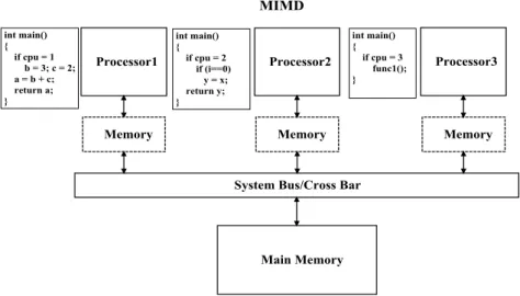
There are many types of parallelism for computing architectures. They are typically classified into four categories, Single-Instruction-Single-Data (SISD), Single-Instruction-Data (SIMD), Multiple-Instruction-Single-Data (MISD), and Multiple-Instruction-Multiple-Data (MIMD), also known as "Flynn's Taxonomy" proposed by Michael J. Flynn [32, 33], shown in Table 2.1. The SIMD process is often used DSP resources to be the hardware to execute parallel data streams; the MISD is un-usually model and rarely used. The MIMD is the most common type in parallel programming by using many processors and SPMD and VLIW are other types of MIMD.
Single Instruction Multiple Instruction
Single Data 1 CPU - 1 program/data SISD 1 CPU - 1 program/data MISD
Multiple Data
SIMD
1 CPU - 1 program/distributed data shared/distrusted memory
MIMD
Multiple CPUs – tasks/distributed data Multiple CPUs – 1 program/distributed data shared/distrusted memory
Table 2.1Flynn’s Taxonomy.
2.2.1
Instruction-Level-Parallelism (ILP)
Instruction sets are implemented in multi-stages in a processor. The overlapped instructions of an N-stage pipeline can be scheduled by N different instruction streams on N clock cycles. A simple Reduced-Instruction-Set-Computing (RISC) processor typically has 5-stage pipeline, I-Fetch, I-Decode, Execute, Memory-Access, and Writeback has shown in Fig 2.2. The longer instruction sets to be paralleled is called Very-Long-Instruction-Word (VLIW), for this action, the hardware resource (ALUs and MULs) are highly required because that multiple operations (eg. addition, multiplication, and loads) often execute at the same time. The VLIW implementation is a type of the ILP that said to multiple instructions being executed concurrently per clock cycle rather than a single set.
_________________________________________________
2.2.2
Data-Level-Parallelism (DLP)
A multi-core processor system performs the same task on distributed data segments across multiple processors simultaneously, which is Data-Level-Parallelism (DLP), also called "data-parallelism". SIMD processors are the majority type of DLP and a vector machine (Datapath) is widely added to support a main CPU to manipulate massive-parallel arithmetic. There is another way of data parallelism: Single-Program-Multiple-Data (SPMD), disturbing databases are implemented in a multi-core processor system and associated separated data are assigned by a conditional statement across each core. SPMD machines are usually utilized to manage large amount of data streams in parallel processing CPUs. The DLP process is widely used in SMPs, the figures and pseudo codes are shown in Fig 2.3.
Figure 2.3Data-parallelsim of SIMD and SPMD.
2.2.3
Thread-Level-Parallelism (TLP)
Thread-Level-Parallelism (TLP) is the most powerful and common model for parallel computing. It is another form of parallelism, comparing to DLP, a program parallelized by functions (or threads) that processes the different task across each core in a multi-processor system simultaneously and each processor executes disturbing process as its instruction is responding (eg. MIMD), which is also called "task-parallelism". Unlike SIMD, the MIMD system is asynchronous paralleling. The associated tasks are also assigned by a conditional statement across each processor, as shown in Fig 2.4. To the memory system, MIMD architectures can be greatly improved in distributed memory. Moreover, the SPMD method is a special case of MIMD, and sometimes people named it as TLP process; however, we normally call it "DLP" instead of TLP across whole sections in this thesis work.
_________________________________________________
Figure 2.4Task-parallelism of MIMD.
2.3
State-of-the-Art in Electronic-System-Level (ESL) Design
Electronic-System-Level (ESL) methodologies are implemented in complex systems for SoC or FPGA designs by using high-level language descriptions to control low-level rather than alone with the traditional RTL approach. This allows designers to optimize performance and area by converting high-level computing functions into hardware circuits; and therefore fast the time to market. The digital designs in five abstraction levels are from high to low: 1) System-level (Structures / Modules), 2) Algorithmic-level (Equations / Behavioural), 3) Register-Transfer-Level (RTL), 4) Gate-level (Netlist), and 5) Layout-level (GDSII). The top-to-down ESL design process is shown in Fig 2.5.
_________________________________________________
At higher levels description, software such as C/C++, and Matlab to describe Functional-Level (micro-architecture) of the architecture components (eg. memories, processors, ALUs and buses) for an entire electronic system; and SystemC (2000) [34] or VHDL to describe Architecture-Level (logic) of functional blocks; and Verilog to describe Implementation-Level (circuit) of gates and wires. In ESL synthesis process, the high-level codes define the structure of the system (behavioural synthesis) and transform un-timed or partially timed functional modules into timed (logic synthesis) RTL implementations which are directly used to create a gate-level description.Many ESL designs are implemented with HW/SW complementary methodologies for custom tradeoffs which a part of C to HDL are compiled and synthesis to generate hardware dataflow; and the rest of the C code is compiled to assembly language as usual in the software. These designs are such as NISC technology (C to Verilog) [35], SPARK (C to VHDL) [36], and LegUp (C to Verilog) [37] toolsets. They are referred to "High-Level-Synthesis (HLS)" frameworks and optimize the HW/SW implementations. However, the design process is the lack of a unified HW/SW representations that invites to the difficulties of modelling, validation, and refinement in the entire system. Generally speaking, the most common modelling language currently used for ESL design is SystemC that is easier to communicate through different abstractions.
2.3.1
Hardware/Software (HW/SW) Co-designs
In Co-design systems, hardware accelerators are separate units from the main processor, which to perform complex computations functions in the hardware. The hardware devices often have outstanding execution timing than the software. The chosen functions that most time spent in the program to perform into RTL hardware datapath to increase the total performance.
_________________________________________________
To this computing methodology, the accelerator and a general-purpose processor running the hardware and software portions of the same programs concurrency and their contingents are able to partitioning; and the systems are able to connect multiple accelerators execute in parallel to enhance the performance, a global cache is typically implemented to slave of connected bus and shared data between accelerators and the processor, as shown in Fig 2.6.However, in this thesis work, I regard to the dual-component of a hardware accelerator / a general-purpose CPU only. Specific examples of hardware accelerators are video card or graphic card in a desktop computer. For the embedded system, HW/SW implementation controls are widely used in ESL / HLS designs and built on many FPGAs or SoC chips.
2.4
FPGA Devices Overview
Previously, I have introduced the fundamental pieces of FPGAs, which are CLBs. The logic blocks wired each other in many different ways to form complex combinational FUs. The modern FPGAs combine hard or soft-core microprocessors, interconnections with the number of CLBs, and related IPs to form a “Programmable SoC”. Nowadays, "Xilinx" and "Altera" are FPGA manufacture leaders and "Lattice" is the third ranked in the world market. To the present high-end FPGA boards, 28 nm layout technology has been utilized on the latest FPGAs version such as Xilinx Virtex-7 and Altera Stratix V with bandwidth up to 2,784 and 28.05 Gb/s respectively; and both of them contain more than 2 million CLBs of equivalent gates [38, 39] that can be fitted to fulfil complex computing and reusable for the designs.
2.4.1
FPGA Fundamental Structures
Imaging a FPGA is a large "memory chip” and software engineers can write some programs to be stored to control it, and let it become a computer. The FPGA hardware architecture consists of a number of, memory blocks, CLBs, DSP units, routing matrix, and I/O pads. The majority hardware device of FPGAs is based on the Static-Memory (SRAM) fabricated in CMOS technology and configuration bitstream can be stored. Since, it is a "volatile" memory type; the data in the gates may lose when the power is switch-off.
There are two types of memory within FPGAs: distributed and block memory. The "distributed memory" is implemented by a number of registers, also named as "CLBs". A number of logic cells form in a CLB. CLBs are the fundamental building blocks of FPGAs that permanently sketch to the hardware target board and depending on different manufactures within different families. The "block memory" is a solid SRAM memory block located on the FPGA floorplan. Furthermore, typically an external FLASH memory for AES encryption stored.
_________________________________________________
The name of Altera CLBs is different, called Logic-Array-Blocks (LABs). A FPGA CLB/LAB contains a number of logic blocks, is called Logic-Cell (LC) in the Xilinx vendor or Logic-Element (LE) in the Altera. LC/LE usages determine the resource cost of a system. The example of the FPGA hierarchical structure has shown in Fig 2.7, based on the Xilinx vendors. A numbers of an N-input Look-Up-Table (LUT) and D-type Flip-Flops (FFs) to construct a "Slice"; and two slices to form a "CLB". For Xilinx Virtex-5/6, a slice consists of 4 LUTs and 4 FFs (1-bit registers). In earlier Xilinx devices, a slice includes only two 4-input LUTs for a combinational logic and two FFs. However, the number of the input for a LUT; and the number of LUTs and FFs per slice can be increased to obtain higher performance. In high-end FPGAs of Virtex-6 families, the 6-input LUT has been manufactured; and four 6-6-input LUTs and FFs have been formed in the slice [40].Figure 2.7FPGA fundamental stuctures.
Moreover, DSP blocks are very dense and special FUs for multiplication arithmetic. Since multiplicand implementations in the LC/LE resource are expensive, use the DSP functionalities efficiently can preserve several hundreds of the logic cells; especially in video / audio data processing applications.
Generally, CLB keeps the same distance each other for the routing and numbers of interconnecting wires are the same in all channels. For Place-and-Route (PAR) synthesis, the routing signals are vertical and horizontal parried with switch boxes at interconnections. An I/O block contains input / output registers, MUXs, and clock signals. FPGA I/O blocks are surrounding the array of CLBs and interface to external components. FPGA clocking resources are clock generation and clock distribution. The clock generator is typically controlled by an analog circuit: Phase-Locked-Loop (PLL) with the Voltage-Controlled-Oscillator (VCO) or digital circuit: Delay-Lock-Loop (DLL) to generate a desired clock phase or frequency. The clock network distributes in global clock lines, regional clocks, and IO clocks. The details of the FPGA clocking resource is not in this research.
_________________________________________________
2.4.2
Advanced FPGA Features
To the higher level view of the FPGA structures, the number of CLBs are reconfigured and interconnected to comprise more compound functionality and several fixed IPs (floorplan) on the silicon, as shown in Fig 2.8. Many vendors develop hard / soft processors or special IPs to realize a customizable processor-system. The advanced FPGA components offer the flexible designed products to meet right requirements, faster time to market, and performance / resource tradeoffs. Moreover, a group of I/O blocks to frame an I/O bank. The I/O bank architecture plays a key role when FPGAs interface other external components. The detail of the FPGA I/O standard is not in this research.
Figure 2.8FPGA advanced stuctures.
Each size of the soft processors / IPs breakdown of FPGA fabric is ordinary pre-estimated to avoid out of resource utilization. As a general rule, the higher resource usage results, the longer routing distance and timing delays between CLBs, and the harder to process the design (synthesis and PAR); these will slower the maximum
_________________________________________________
system clock. It can be solved by placing registers along the datapath to balance delays between registers, however, it will may increase the size of the design still and most of the soft IP cores design tool do not provide this technique. InFig 2.9
, it is shown that the longest wiring (routing) delay determines the maximum frequency on an FPGA.Figure 2.9The routing delays and maximum frequency within FPGAs.
In general, for FPGA resource estimation, it is recommended to overestimate the total resource usage may be mapped onto FPGA boards. Typically said < 50% FPGA utilization of the initial estimation, because the prototyping will may change and some diagnostics logic may will be added in further. Moreover, each CLB may difficult to wire together in the PAR and degrade the execution time of the programs when devices are too full of the logic cells, and said < 75% FPGA utilization of the final design [41].
2.5
Embedded Processors on FPGAs
There are two types of the embedded processors on the FPGA-based designs: hard and soft cores. To compare soft vs hard-core on FPGA devices, the advantage of the soft-processors are utilized standard mass-produced, the lower FPGA devices cost, and the numbers of cores are customizable. However, the disadvantages are lower processor performance, higher power consumption, and larger area, because in the most part that there are breakdown most of the LC/LE resource (eg. MicroBlaze occupies around 1,200-5,000 LUTs on Xilinx FPGAs and PowerPC is a fixed gate-level IP) within the FPGA.
Through the embedded processors modern today, there are increasing interest for the "more than one core" system designs in one chip die in order to accomplish superior performance. There are three sorts of combinations to attain more than one core system: "Multi-core Processor (Homogeneous)", "Co-design Processor (Hardware/Software)", and "Multi-core Processor (Heterogeneous)". The ideal example of those architectures and prototypes are represented in Fig 2.10.
_________________________________________________
Figure 2.10Embedded processor-systems.
To increase computational purposes by the hardware accelerator to perform function-complex programming (HLS), the Co-design system is appropriate to be used. The most common system of the multi-core processor is homogeneous; the processors are from the same manufactured and easily to be constructed. Homogeneous multi-processor system are favourable to be utilized in "data-parallelism". The most progressive system is the heterogeneous multi-processor, because each of the processors can match different applications to that core is best suited to be executed; thereupon to meet ultimate performance [42]. Heterogeneous multi-core processor are facilitated in "task-parallelism". However, they are hardly to be built up, due to very complex design tools of the software compatibility of the mixture IP components. To this thesis work, I only concern the homogeneous case in the study.
_________________________________________________
2.5.1
Hard and Soft Processors
The hard-core also refers to ASIC processors, such as Power PC 440 and ARM Cortex-A9 are embed "physical" core and dedicated part of the integrated circuit (floorplan) into the FPGA silicon. The popular fabricated hard-core CPUs on FPGAs are presented in Table 2.2.
Processor Developer Architecture Bits Pipeline Stages
L1/L2 Cache( KB)
MMU FPU Clock
rate/MHz Area/𝐦𝐦𝟐 PowerPC 440 AMCC Power Architecture 32 7 32/256
ˇ
ˇ
667 6.0 PowerPC 460 AMCC Power Architecture 32 7 32/256ˇ
ˇ
600~1000 1.23Cortex-A7 ARM ARMv7-A 32 8 8~64/1000
ˇ
ˇ
>1000 0.45Cortex-A9 ARM ARMv7-A 32 8 ?/8000
ˇ
ˇ
830 1.54KEc MIPS MIPS32 32 5 Instruction/
Data 8/8
ˇ
ˇ
233 2.54Kc MIPS MIPS32 32 5 Instruction/
Data 8/8
ˇ
ˇ
190 3.42Table 2.2Embedded hard-cores on FPGAs [43 - 46].
The soft-core also refers to FPGA processors, such as MicroBlaze, NIOS II, and LEON3/4 are built in “reconfigurable" and "synthesizable" cores then fit into the FPGA logic "fabric". They are frequently open-source / proprietary with IUs, and optional MMU and FPUs [47]. In Table 2.3, outline the well known manufactures soft-core CPUs suitable on the FPGAs.
Processor Developer Architecture Bits Bus Support
Pipeline Stages
MUL FPU Cache MMU Area
(LUTs)
MicroBlaze Xilinx MicroBlaze 32 PLB, OPB,
FSL, LMB, 3, 5 opt opt
ˇ
opt1,200-5,000
PicoBlaze Xilinx PicoBlaze 8 no
˟
˟
˟
˟
190Nios II/f Altera Nios II 32 Avalon 6
ˇ
optˇ
ˇ
1,800LEON2 ESA SPARC-V8 32 AMBA2 5
ˇ
extˇ
ˇ
5,000LEON3/4 Aeroflex
Gaisler SPARC-V8 32 AMBA2 7
ˇ
ˇ
ˇ
ˇ
3,500-6,000 LatticeMico32 Lattice LatticeMico32 32 Wishbone 6 opt
˟
ˇ
˟
~2,400Cortex-M1 ARM ARMv6 32 AMBA2 3
![Figure 4.2 LEON3 CPU core IU datapath [64].](https://thumb-us.123doks.com/thumbv2/123dok_us/10222980.2926181/51.892.139.748.105.732/figure-leon-cpu-core-iu-datapath.webp)
![Table 5.1 LEON3 blocks CONFIGURABILITY [64].](https://thumb-us.123doks.com/thumbv2/123dok_us/10222980.2926181/67.892.121.780.713.1053/table-leon-blocks-configurability.webp)