N A N O E X P R E S S
Open Access
Optical Properties of Al-Doped ZnO Films
in the Infrared Region and Their Absorption
Applications
Hua Zheng
1,2, Rong-Jun Zhang
1*, Da-Hai Li
1, Xin Chen
2*, Song-You Wang
1, Yu-Xiang Zheng
1, Meng-Jiao Li
3,
Zhi-Gao Hu
3, Ning Dai
2and Liang-Yao Chen
1Abstract
The optical properties of aluminum-doped zinc oxide (AZO) thin films were calculated rapidly and accurately by point-by-point analysis from spectroscopic ellipsometry (SE) data. It was demonstrated that there were two different physical mechanisms, i.e., the interfacial effect and crystallinity, for the thickness-dependent permittivity in the visible and infrared regions. In addition, there was a blue shift for the effective plasma frequency of AZO when the thickness increased, and the effective plasma frequency did not exist for AZO ultrathin films (< 25 nm) in the infrared region, which demonstrated that AZO ultrathin films could not be used as a negative index metamaterial. Based on detailed permittivity research, we designed a near-perfect absorber at 2–5μm by etching AZO-ZnO alternative layers. The alternative layers matched the phase of reflected light, and the void cylinder arrays extended the high absorption range. Moreover, the AZO absorber demonstrated feasibility and applicability on different substrates.
Keywords:Aluminum-doped zinc oxide, Infrared, Spectroscopic ellipsometry, Absorber
Background
Plasmonics [1] and metamaterials [2] have attracted much attention in recent decades. Many unconventional functionalities, such as negative refractive index mate-rials [3], sub-diffraction imaging [4], and invisibility cloaks [5], were presented, which conventionally used noble metals as the primary plasmonic building blocks of optical metamaterials [6]. Compared with noble metals, heavily doped semiconductors, such as aluminum-doped zinc oxide (AZO) [7] and titanium ni-tride (TiN) [8], have recently played a more important part in plasmonics and metamaterial applications be-cause of their tunable free carrier concentrations. The doping density [8], growth atmosphere, and the growth or annealing temperature [9] were the usual methods to adjust the properties of heavily doped semiconductors. As a heavily doped semiconductor with broad band gap,
AZO is a tunable, low-loss plasmonic material capable of supporting high dopant concentrations, and it plays an important role in plasmonic structures [10]. For ex-ample, a material system such as zinc oxide (ZnO) and AZO has an evident advantage as a result of the epitaxial and superlattice design of the device structure, which can reduce the losses at the layer interfaces and thus fur-ther boost the device performance [11–16]. Although many papers [17, 18] have focused on the properties of AZO in the visible or near-infrared region, only a few have concentrated on the infrared properties of AZO, which influence the realistic applications. Recently, Upr-ety et al. [19] discussed the optical properties of bulk AZO by means of recombination model simulation of spectroscopic ellipsometry (SE). The simulation was gen-eral but not rapid or convenient. In this paper, we calcu-lated the permittivity of AZO thin films from 210 to 5000 nm by means of point-by-point analysis [20], a cal-culation dependent on primary SE simulation, which is a rapid and accurate method. In addition, we discussed the reasons for the thickness-dependent properties of AZO thin films in the visible and infrared bands with two different mechanisms, respectively. The thickness
* Correspondence:[email protected];[email protected] 1Key Laboratory of Micro and Nano Photonic Structures, Ministry of
Education, Department of Optical Science and Engineering, Fudan University, Shanghai 200433, China
2National Laboratory for Infrared Physics, Shanghai Institute of Technical
Physics, Chinese Academy of Sciences, Shanghai 200083, China Full list of author information is available at the end of the article
dependence of the band gap and effective plasma fre-quency of AZO were also demonstrated. We found the effective plasma frequency does not exist with low thick-ness (< 25 nm) in the infrared region. Furthermore, we used finite difference time domain (FDTD) solutions to design two void cylinder arrays based on AZO alterna-tive layers, which demonstrated near perfect absorption in infrared broadband.
Methods
Since existing atomic layer deposition (ALD) shows ul-trahigh conformity and compatibility to semiconductor processing [21], it is a powerful tool for plasmonic ma-terial deposition with precisely controlled thickness. AZO thin films were deposited on p-type Si (100) by al-ternating diethylzinc (Zn(CH2CH3)2, DEZ; Al(CH3)3, TMA) and deionized water (H2O) in an ALD reactor (Picosun) at 190 °C. A typical ALD cycle for AZO con-sisted of 14 single cycles ZnO and 1 single cycle Al-O, while the single cycle of ZnO or Al-O consisted of 0.1 s DEZ or TMA pulse, 5 s N2purge, 0.1 s H2O pulse, and 5 s N2purge according to our previous reports [22–24]. The mechanism of ZnO ALD is the chemical vapor de-position reaction.
Zn CHð 2CH3Þ2þH2O→ZnOþ2C2H6 ð1Þ
There are two reactions in an ALD cycle.
ZnOHþZn CHð 2CH3Þ2→ZnOZn CHð 2CH3ÞþC2H6
ð2Þ
Zn CHð 2CH3ÞþH2O→ZnOHþC2H6 ð3Þ
And the Al doping is similar, where the cycle of Zn:Al is 14:1.
AlOHþAl CHð 3Þ3→AlOAl CHð 3Þ2
þCH
4 ð4Þ
AlOAl CHð 3Þ2
þ
2H2O→AlOAlOHþ2CH4 ð5Þ
where * indicates a surface species.
Here, the thickness of AZO thin films was varied by controlling ALD cycles. There were three types of sam-ples: 150, 300, and 450 cycles (here we used the funda-mental single cycle as the unit of measurement). The thicknesses and optical properties of ZnO ultrathin films were obtained by a spectroscopic ellipsometer (J.A. Woollam, USA). The incident angle was fixed at 65° and
[image:2.595.305.539.87.405.2]the wavelength ranged from 210 to 1000 nm, 1000 to 2000 nm, and 2000 to 5000 nm. The reflection and transmission of AZO films were obtained by Fourier transform infrared spectroscopy (FTIR) measurements. X-ray diffraction (XRD) patterns suggested the optical properties changed with the thickness of the AZO films.
Table 1Thickness of AZO films simulated by SE and measured by SEM, respectively
Methods 150 cycles 300 cycles 450 cycles
SE (nm) 26.0 50.3 75.6
SEM (nm) 24.8 47.3 75.4
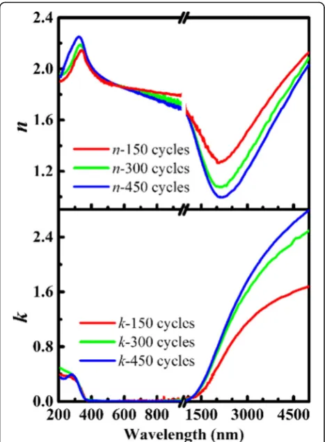
Fig. 1Refractive index (n) and extinction coefficient (k) were simulated by point-by-point analysis using the data from SE measurements
[image:2.595.306.537.543.703.2] [image:2.595.57.290.690.732.2]Results and Discussions
Optical Properties of AZO Films in Visible and Infrared Broadband
Due to low interfacial roughness by ALD, the monolayer model was used to describe the AZO thin films [10]. Then, the refractive index n, extinc-tion coefficient k and thickness d of the resulting AZO thin films were obtained by the SE measure-ment. During the SE measurement [25, 26], the el-liptically polarized light, carrying the material’s information after reflected by AZO films, was de-tected by the ellipsometer. The wavelength of the incident light was within the range of 210– 5000 nm. There are two measurement parameters acquired from the polarized light, i.e., amplitude ra-tio (Ψ) and phase shift (Δ), which were defined by the ellipsometric ratio ρ as [27]:
ρ¼rp rs ¼
tanΨejΔ ð6Þ
Here rpand rs are the complex reflection coefficients of polarized light parallel and perpendicular to the inci-dence plane, respectively. For SE fittings, the root mean square error (RMSE) is minimized to obtain an accuracy fitting:
RMSE¼
ffiffiffiffiffiffiffiffiffiffiffiffiffiffiffiffiffiffiffiffiffiffiffiffiffiffiffiffiffiffiffiffiffiffiffiffiffiffiffiffiffiffiffiffiffiffiffiffiffiffiffiffiffiffiffiffiffiffiffiffiffiffiffiffiffiffiffiffiffiffiffiffiffiffiffiffiffiffiffiffiffiffiffiffiffiffiffiffiffiffiffi 1
2x−y−1 X
x
i¼1 Ψcali −Ψexpi
2
þ Δcal i −Δexpi
2
h i
s
ð7Þ
Herexis the number of data points in the spectra,yis the number of variable parameters in the model, and
“exp” and “cal” represent the experimental and the cal-culated data, respectively [28]. In the previous report [22], we used the Forouhi-Bloomer (F-B) dispersion model to fit ellipsometry parameters of ZnO at 300– 800 nm. Due to the metallic properties of AZO, how-ever, the F-B model is not suitable for AZO films in the whole spectrum from 200 to 5000 nm, which is a model only for single electron transition [29]. Considering the transparency and metallicity of AZO, the Cauchy model is appropriate for the spectrum of 400–800 nm and the Drude-Lorentz model is appropriate for the infrared (1500–5000 nm) [7, 17]. We obtained the thickness and initial parameters ofnandkof AZO thin films from the lowest RMSE of the simulation data as shown in Table1, where the SEM results were consistent with the SE simulation. Furthermore, a point-by-point analysis [20] was used to calculate the n and k at the whole wave-length, and the results are presented in Fig.1. There are two regions ofnandk, which are separated by switching the SE working range. Also, the fitting results can be di-vided into two regions, i.e., the visible region and the in-frared region. In the visible region (210–800 nm), the value of n and k of AZO was approximate to ZnO for the low percentage of Al. The nand kin the visible re-gion indicate regular semiconductor properties. The value of k is near to zero in the visible range and n is thickness-dependent. Here, the thickness dependence was explained by the interface effect [22], which plays an important part in thin films. For the silicon substrate, the interface effect results in the lower permittivity of AZO thinner films in the visible range. However, the trend of n and k was changed in the infrared region Fig. 3XRD patterns of the AZO thin films with different thicknesses
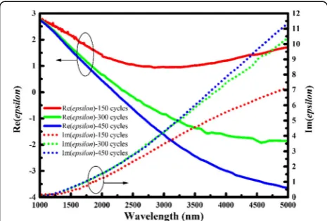
Fig. 4The real part and imaginary part of epsilon of AZO films with different thicknesses, which was calculated fromnand
[image:3.595.58.290.87.263.2]k(εer¼n2−k2þi2nk)
Table 2Wavelength when the real part of epsilon of AZO thin films is zero in Fig.4
150 cycles 300 cycles 450 cycles
Wavelength (nm) / 2390 2204
[image:3.595.302.539.110.151.2] [image:3.595.57.290.534.691.2](800–5000 nm). With the increasing of the wavelength,
k increased from zero, which is the huge difference be-tween AZO and ZnO. The increase ofkindicated the in-crease of the film absorption, and the AZO film cannot be used as transparent dielectric material in infrared. There are metallic properties of AZO in the infrared re-gion, which is not only a semiconductor but also a metal material in the infrared region. Moreover, a Hall meas-urement indicated the bulk carrier concentration of AZO was approximately 1.9 × 10²¹/cm3. The high concentration refers to the existence of free electrons, because of Al dopant. An opposite thickness dependence was shown in infrared. The mechanism of the thickness dependence is not the same in the infrared region. The
interface effect remains, but the impact is no longer important due to the narrower differences in permittivity between AZO and interface layer while the permittivity of AZO is low in the infrared region. It is assumed that the permittivity of AZO was also influenced by the thickness-dependent crystallinity, which influenced the polarization of AZO thin films.
Furthermore, a linear extrapolation to (αE) 2= 0 was used at the absorption edge to obtain the band gap of AZO films in Fig. 2, where α is the absorption coefficient (α= 4πk/λ) and E is the photon energy [28]. The high energy of the absorption edge of AZO results from the free electron screening effect [16], which suppresses the excitonic absorption. The table in Fig. 2 indicates a blue shift of the band gap (Eg) of AZO from 3.62 to 3.72 eV.
Moreover, XRD was supposed to measure the crystal-linity of AZO films. Figure 3 gives the XRD patterns of the AZO thin films with different thickness. Compared with ZnO films, AZO films are not very crystallographic, as a result of the Al doping. The obvious crystal peak is (100) in the sample with 450 cycles, which represents the hexagonal wurtzite phase of polycrystalline ZnO [30, 31]. Thermal annealing does have an effect on the crys-talline property, and this has been discussed elsewhere [7, 9, 10, 22, 32]. The thickness-dependent crystallinity can be used to explain the SE results. The higher crystal-linity means the fewer lattice defects, and film stress and strain, which contributes to the blue shift of band gap, higher carrier concentration, and polarization.
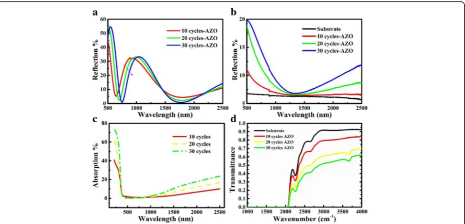
In conclusion, the AZO films were not highly crystal-lized and the crystallinity depended on the thickness, Fig. 5aReflection of AZO films on Si substrate;bReflection,cabsorption, anddtransmittance of AZO films on SiO2substrate
[image:4.595.61.539.87.318.2] [image:4.595.57.290.532.702.2]which resulted in a blue shift of band gap and the change in permittivity.
On the other hand, we changednandkinto permittivity εr(εer¼n2−k2þi2nk), and the real imaginary parts of
εr are illustrated in Fig. 4. The real part of εr decreases with the thickness increasing when the imaginary part of εrincreases. In specific terms, the real part ofεris negative in some regions of the spectrum, and the point when the real part of epsilon trends to zero exists. In line with the metallic properties of metal described by the Drude model, the frequency when the real part of epsilon trends to zero is called plasma frequency. Table2illustrates that the effective plasma frequency of AZO has a blue shift when the thickness increases. Moreover, for the lower thickness sample, 150-cycle AZO films, the zero point does not exist in the infrared region. In brief, thickness in-fluences the permittivity of AZO, and the real part of epsi-lon of AZO ultrathin films is always positive. In another word, AZO films could not be regarded as a metamaterial at ultrathin thickness, where the negative real part of epsi-lon is of importance in plasmonic applications [12].
Figure 5 illustrates the reflection, absorption, and transmission of investigated AZO films. Figure 5a, b il-lustrate the reflection of AZO films on Si and SiO2 sub-strates, respectively. It was found that there is higher reflection on the higher thickness of AZO on SiO2 sub-strate. The low reflection of AZO on SiO2 substrate in 1000–1500 nm results from low nand k in Fig.1. The absorption data in Fig. 5c were calculated from the re-flection and transmission. It is assumed that the sum of absorption, reflection, and transmission is equal to 1. The absorption curves in Fig. 5c illustrate that the ab-sorption of AZO films is thickness-dependent in the in-frared region, which is consistent to the SE calculation and analysis. The transmission curves in Fig. 5d were measured by FTIR. Between 2500 and 5000 nm (equal to 4000–2000 cm−1), there is lower transmission in the thicker AZO films.
Near Perfect Absorption Application by Void Cylinder Arrays on AZO Alternative Layers
AZO is usually used instead of noble metals as a low-loss plasmonic material in the infrared region [12], but it is also appropriate to build a high absorber in infrared broadband in view of its comparatively lower extinction coefficient, as indicated in Fig.6.
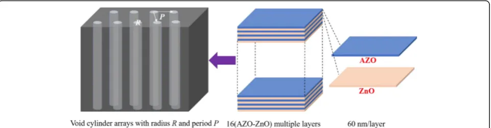
In our earlier work [11], 32 layers of AZO/ZnO alter-native films were deposited on silicon or quartz sub-strate by ALD. The thickness of 32-layer alternative films is approximately 1.92μm, each layer being 60 nm thick. The alternative layers were used to design absorp-tion structures due to near-perfect absorpabsorp-tion at ~ 1. 9 μm. We took the parameters of AZO thin films from Fig. 7The structure of void cylinder arrays on AZO/ZnO alternative layers. The radius of the void cylinder arrays isRμm, and the period isPμm. The thickness of 32 layers of AZO/ZnO alternative films is approximately 1.92μm, each layer being 60 nm thick
[image:5.595.59.540.88.214.2]Fig. 8Reflection and absorption of array A and array B
Table 3Parameters of arrays in Fig.8
Parameters Radius (μm) Period (μm) The highest absorption
Array A 0.6 1.8 0.967
[image:5.595.58.289.560.712.2] [image:5.595.305.539.688.731.2]the SE analysis and those of ZnO thin films from our earlier work, then used FDTD solutions as the simula-tion software to simulate the absorpsimula-tion of the arrays with different parameters. Figure 7 illustrates the ab-sorber structure built by void cylinder arrays on AZO/ ZnO alternative layers. The radius of the void cylinder arrays isRμm and the period isPμm.
As a result, Fig.8presents two kinds of arrays for high absorption and low reflection at a range of between 2 and 5 μm. The specific data are presented in Tables 3 and 4. For array A, the radius is 0.6μm and the period is 1.8 μm; for array B, the radius is 0.8 μm and the period is 2.0 μm. Array B has broadband absorption of between 2.04 and 5μm, in which the absorption is more than 0.9. Array A has better absorption than array B in the near-infrared. The negative real part of permittivity of AZO allows the alternating layers to match the phase of all reflected light while the periodic arrays and low permittivity contribute to the infrared broadband.
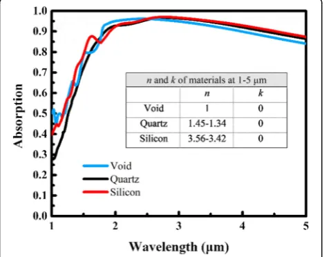
Figure9indicates the absorption of absorber A on dif-ferent substrates in the infrared region. The void, silicon, and quartz are all transparent in the infrared region. While the refractive indexnchanges from 1 to 3.56, the absorption changes little, which demonstrates the feasi-bility and applicafeasi-bility of the structure.
Conclusions
In summary, we examined the thickness-dependent properties of AZO films and designed an AZO infrared
broadband absorber. The thickness of AZO films influ-ences permittivity in both the visible and infrared re-gions. There are two different physical mechanisms, interface effect and thickness-dependent crystallinity, that lead to thickness-dependent permittivity. Further-more, there is a blue shift for the effective plasma fre-quency of AZO with an increase in thickness, which does not exist with low thickness (< 25 nm) in the infra-red region. These two thickness-dependent properties demonstrate a new method adjusting the thickness to modulate the properties of AZO thin films and indicate that the AZO ultrathin film cannot be used as a meta-material. Based on AZO permittivity properties, we designed near-perfect infrared arrays by using 32 alter-native layers of AZO and ZnO. The negative real part of permittivity of AZO allows the alternative layers to match the phase of all reflected light while the periodic arrays and low permittivity contribute to the infrared broadband. Moreover, the AZO absorber demonstrates feasibility and applicability on different substrates. It is be-lieved that these investigations contribute to a better un-derstanding of the optical properties of AZO thin films in the visible and infrared region for optical and plasmonic applications and that they demonstrate the possibility and feasibility of the AZO absorber at 2–5μm.
Abbreviations
ALD:Atomic layer deposition; AZO: Aluminum-doped zinc oxide; F-B: Forouhi-Bloomer; FDTD: Finite difference time domain; FTIR: Fourier transform infrared spectroscopy; RMSE: Root mean square error; SE: Spectroscopic ellipsometry; SiO2: Silicon dioxide; XRD: X-ray diffraction; ZnO: Zinc oxide
Acknowledgements
This work has been supported by Key Laboratory of Infrared Imaging Materials and Detectors, Shanghai Institute of Technical Physics, Chinese Academy of Sciences and Key Laboratory of Polar Materials and Devices, Ministry of Education, Department of Electronic Engineering, East China Normal University.
Funding
National Natural Science Foundation of China (Nos. 11674062, 61376016, and 61427815), National Science and Technology Major Project of China (No. 2011ZX02109-004), Ministry of Science and Technology of the People’s Republic of China (No. 2016YFE0110700), Science and Technology Commission of Shanghai Municipality Project of China (No. 12XD1420600).
Authors’Contributions
[image:6.595.57.543.99.141.2]HZ performed the experiment of the AZO thin films, designed the AZO absorber, and drafted the manuscript. RJZ and XC proposed the initial work and finalized the manuscript. DHL, MJL, and ZGH provided guidance and assistance in the experiment. SYW and YXZ participated in the design and coordination of the study. ND and LYC supervised the work. All authors have read and approved the final manuscript.
Table 4High absorption band of arrays in Fig.8
Absorption band X (μm) X1= 0.8 X2= 0.9 X3= 0.9 X4= 0.8 X4–X1 X3–X2
Array A 1.61 1.84 4.33 > 5 > 3.39 2.49
Array B 1.64 2.04 > 5 > 5 > 3.36 > 2.96
[image:6.595.57.292.519.705.2]Competing Interests
The authors declare that they have no competing interests.
Publisher’s Note
Springer Nature remains neutral with regard to jurisdictional claims in published maps and institutional affiliations.
Author details 1
Key Laboratory of Micro and Nano Photonic Structures, Ministry of Education, Department of Optical Science and Engineering, Fudan University, Shanghai 200433, China.2National Laboratory for Infrared Physics, Shanghai Institute of Technical Physics, Chinese Academy of Sciences, Shanghai 200083, China.3Key Laboratory of Polar Materials and Devices, Ministry of Education, Department of Electronic Engineering, East China Normal University, Shanghai 200241, China.
Received: 5 March 2018 Accepted: 30 April 2018
References
1. Lal S, Link S, Halas NJ (2007) Nano-optics from sensing to waveguiding. Nat Photonics 1(11):641–648
2. Smith DR, Pendry JB, Wiltshire MCK (2004) Metamaterials and negative refractive index. Science 305(5685):788–792
3. Soukoulis CM, Linden S, Wegener M (2007) Negative refractive index at optical wavelengths. Science 315(5808):47–49
4. Liu ZW, Lee H, Xiong Y, Sun C, Zhang X (2007) Far-field optical hyperlens magnifying sub-diffraction-limited objects. Science 315(5819):1686–1686 5. Cai WS, Chettiar UK, Kildishev AV, Shalaev VM (2007) Optical cloaking with
metamaterials. Nat Photonics 1(4):224–227
6. Wang Z, Zhang R, Guo J (2018) Quadrupole mode plasmon resonance enabled subwavelength metal-dielectric grating optical reflection filters. Opt Express 26(1):496–504
7. Lin JY, Zhong KD, Lee PT (2016) Plasmonic behaviors of metallic AZO thin film and AZO nanodisk array. Opt Express 24(5):5125–5135
8. Naik GV, Schroeder JL, Ni X, Kildishev AV, Sands TD, Boltasseva A (2012) Titanium nitride as a plasmonic material for visible and near-infrared wavelengths. Opt Mater Express 2(4):478–489
9. Li XD, Chen TP, Liu Y, Leong KC (2014) Evolution of dielectric function of Al-doped ZnO thin films with thermal annealing: effect of band gap expansion and free-electron absorption. Opt Express 22(19):23086–23093
10. Riley CT, Smalley JS, Post KW, Basov DN, Fainman Y, Wang D, Liu Z, Sirbuly DJ (2016) High-quality, ultraconformal aluminum-doped zinc oxide nanoplasmonic and hyperbolic metamaterials. Small 12(7):892–901 11. Zhang Y, Wei T, Dong W, Huang C, Zhang K, Sun Y, Chen X, Dai N (2013)
Near-perfect infrared absorption from dielectric multilayer of plasmonic aluminum-doped zinc oxide. Appl Phys Lett 102(21):213117
12. Naik GV, Liu J, Kildishev AV, Shalaev VM, Boltasseva A (2012) Demonstration of Al:ZnO as a plasmonic component for near-infrared metamaterials. Proc Natl Acad Sci U S A 109(23):8834–8838
13. Li X, Jiao L, Xu H, Lu Y, Zhu C, Duan J, Zhang X, Dai N, Song W (2016) Near-infrared subwavelength imaging using Al:ZnO-based near-field superlens. Opt Mater Express 6(12):3892
14. Ferrari L, Wu C, Lepage D, Zhang X, Liu Z (2015) Hyperbolic metamaterials and their applications. Prog Quantum Electron 40:1–40
15. Cui Y, Fung KH, Xu J, Ma H, Jin Y, He S, Fang NX (2012) Ultrabroadband light absorption by a sawtooth anisotropic metamaterial slab. Nano Lett 12(3):1443–1447
16. Li XD, Chen TP, Liu P, Liu Y, Leong KC (2013) Effects of free electrons and quantum confinement in ultrathin ZnO films: a comparison between undoped and Al-doped ZnO. Opt Express 21(12):14131
17. Li QH, Zhu D, Liu W, Liu Y, Ma XC (2008) Optical properties of Al-doped ZnO thin films by ellipsometry. Appl Surf Sci 254(10):2922–2926 18. Ehrmann N, Reineke-Koch R (2010) Ellipsometric studies on ZnO:Al thin
films: refinement of dispersion theories. Thin Solid Films 519(4):1475–1485 19. Uprety P, Junda MM, Ghimire K, Adhikari D, Grice CR, Podraza NJ (2017)
Spectroscopic ellipsometry determination of optical and electrical properties of aluminum doped zinc oxide. Appl Surf Sci 421:852–858
20. Li DH, Zheng H, Wang ZY, Zhang RJ, Zhang H, Zheng YX, Wang SY, Zhang DW, Chen LY (2017) Dielectric functions and critical points of
crystalline WS2ultrathin films with tunable thickness. Phys Chem Chem Phys 19(19):12022–12031
21. Shi YJ, Zhang RJ, Zheng H, Li DH, Wei W, Chen X, Sun Y, Wei YF, Lu HL, Dai N, Chen LY (2017) Optical constants and band gap evolution with phase transition in sub-20-nm-thick TiO2 films prepared by ALD. Nanoscale Res Lett 12(1):243
22. Zheng H, Zhang R-J, Xu J-P, Wang S-X, Zhang T-N, Sun Y, Zheng Y-X, Wang S-Y, Chen X, Chen L-Y, Dai N (2016) Thickness-dependent optical constants and annealed phase transitions of ultrathin ZnO films. J Phys Chem C 120(39):22532–22538
23. Zhai CH, Zhang RJ, Chen X, Zheng YX, Wang SY, Liu J, Dai N, Chen LY (2016) Effects of Al doping on the properties of ZnO thin films deposited by atomic layer deposition. Nanoscale Res Lett 11(1):407
24. Wang ZY, Zhang RJ, Lu HL, Chen X, Sun Y, Zhang Y, Wei YF, Xu JP, Wang SY, Zheng YX, Chen LY (2015) The impact of thickness and thermal annealing on refractive index for aluminum oxide thin films deposited by atomic layer deposition. Nanoscale Res Lett 10:46
25. Wang Z, Yuan S, Li D, Jin F, Zhang R, Zhan Y, Lu M, Wang S, Zheng Y, Guo J, Fan Z, Chen L (2016) Influence of hydration water on CH3NH3PbI3 perovskite films prepared through one-step procedure. Opt Express 24(22): A1431–A1443
26. Zhang R-J, Chen Y-M, Lu W-J, Cai Q-Y, Zheng Y-X, Chen L-Y (2009) Influence of nanocrystal size on dielectric functions of Si nanocrystals embedded in SiO2matrix. Appl Phys Lett 95(16):161109
27. Xia GQ, Zhang RJ, Chen YL, Zhao HB, Wang SY, Zhou SM, Zheng YX, Yang YM, Chen LY, Chu JH, Wang ZM (2000) New design of the variable angle infrared spectroscopic ellipsometer using double Fourier transforms. Rev Sci Instrum 71(7):2677–2683
28. Xu J-P, Zhang R-J, Zhang Y, Wang Z-Y, Chen L, Huang Q-H, Lu H-L, Wang S-Y, Zheng Y-X, Chen L-Y (2016) The thickness-dependent band gap and defect features of ultrathin ZrO2films studied by spectroscopic ellipsometry. Phys Chem Chem Phys 18(4):3316–3321
29. Forouhi AR, Bloomer I (1988) Optical properties of crystalline semiconductors and dielectrics. Phys Rev B 38(3):1865–1874 30. Abou Chaaya A, Viter R, Bechelany M, Alute Z, Erts D, Zalesskaya A,
Kovalevskis K, Rouessac V, Smyntyna V, Miele P (2013) Evolution of microstructure and related optical properties of ZnO grown by atomic layer deposition. Beilstein J Nanotech 4:690–698
31. Díez-Betriu X, Jiménez-Rioboo R, Marcos JS, Céspedes E, Espinosa A, de Andrés A (2012) Amorphous-nanocrystalline Al doped ZnO transparent conducting thin films. J Alloys Compd 536:S445–S449
32. Ohta N, Ohba D, Sato S, Tang Z, Shimizu H, Shirai H (2011) Rapid thermal-plasma annealing of ZnO:Al films for silicon thin-film solar cells. Thin Solid Films 519(20):6920–6927
33. Olmon RL, Slovick B, Johnson TW, Shelton D, Oh S-H, Boreman GD, Raschke MB (2012) Optical dielectric function of gold. Phys Rev B 86:23