International Journal of Emerging Technology and Advanced Engineering
Website: www.ijetae.com (ISSN 2250-2459,ISO 9001:2008 Certified Journal, Volume 4, Issue 8, August 2014)
32
High-Order CCII-Based Mixed-Mode Universal Filter
Chen-Nong Lee
Department of Computer and Communication Engineering, Taipei Chengshih University of Science and Technology, Taipei, Taiwan, R. O. C.
Abstract— This paper presents a new high-order
mixed-mode (including voltage, current, transadmittance, and transimpedance modes) universal filter structure using n+1 second-generation current conveyors (CCIIs), n grounded capacitors and n+2 resistors, which are the minimum number of active component counts for realizing an nth-order mixed-mode universal filtering responses (low-pass, high-pass, band-pass, band-reject, and all-pass) from the same topology. Many important advantages are simultaneously achieved which are (i) using only CCIIs (with simpler implementation configuration than the differential difference current conveyors (DDCCs) and fully differential current conveyors (FDCCIIs)), (ii) all grounded capacitors (attractive for integration), (iii) high output impedance for current output (good for cascadability), (iv) no need to impose component choice except the voltage and transadmittance all-pass response, (v) no need of inverting-type input signals or double-type input signals for the use of special input signals, and (vi) low sensitivity performance. H-Spice simulation results confirm the theory.
Keywords—Active filters, second-generation current
conveyors, mixed-mode, high-order filter, universal filter.
I. INTRODUCTION
Over the last decade, many high-order voltage-mode or current-mode filters have been presented in the literature [1-17]. From historical progress point of view, we might intend to replace the traditional voltage-mode circuits with the more precise current-mode circuits. There might be a transferring period from voltage-mode to current-mode world. Then, the transadmittance (i.e. input as voltage and output as current) and transimpedance (i.e. input as current and output as voltage) modes will be involved in that between voltage and current modes, and therefore, play a very important role in the special filtering applications where we need to connect a voltage-mode circuit with a current-mode circuit and vice versa. Hence, in analog signal processing applications, we may be desirable to have active filter with input currents or voltages and output currents and voltages, defined as mixed-mode filter.
Therefore, the mixed-mode (including voltage, current, transadmittance, and transimpedance modes) circuits are worthy of researches and presented for the use of any filtering requirement which is compatible with modern microelectronic systems applications, such as controls and voice and data communications, where consideration of size and weight make the use of inductors prohibitive.
Although many mixed-mode biquad filters have been proposed, few high-order mixed-mode filters have been
presented in the literature [15, 18-20]. In 2009, an nth-order
mixed-mode filter was proposed [19]. The filter structure
[19] employs n+2 operational transconductance amplifiers
(OTAs) and n grounded capacitors, which can realize n
th-order mixed-mode (including voltage, current,
transadmittance, and transimpedance modes) universal filtering responses (low-pass, high-pass, pass, band-reject, and all-pass) from the same topology. However, the structure [19] offers three following disadvantages: (i) need of extra inverting amplifiers for realizing voltage and transadmittance modes allpass signals, (ii) need of the two
same nth input current (In) for constructing current output
and voltage output, and (iii) inconvenient input currents settings for realizing current and transimpedance modes highpass, bandreject, and allpass signals. Therefore, in
2012, a new nth-order mixed-mode filter was proposed [20].
The structure, reported in [20], can overcome the above
three disadvantages but it need to use n+3 active elements
(i.e. OTAs) in addition to n grounded capacitors. Although
the nth-order mixed-mode structure reported in [18] uses
only n+1 active elements (i.e. DDCCs) in addition to n
grounded capacitors and n+2 resistors, the DDCCs are
more complex active elements than CCIIs. In 2009, a good
high-order current-mode and transimpedance-mode
universal filter was proposed in [15]. The filter [15]
employs only n+1 active elements (i.e. multiple outputs
CCIIs (MOCCIIs)) in addition to n grounded capacitors
and n+1 resistors but it can not be used in voltage and
International Journal of Emerging Technology and Advanced Engineering
Website: www.ijetae.com (ISSN 2250-2459,ISO 9001:2008 Certified Journal, Volume 4, Issue 8, August 2014)
33
Therefore, this leads to prospective research work: investigating and developing a high-order mixed-mode
(including voltage, current, transadmittance, and
transimpedance modes) universal filter structure using
reduced number (no more than n+1) of active components
which have the simpler structure than DDCC. In this paper, the proposed high-order mixed-mode universal filter uses
only n+1 CCIIs (with the simpler structure than DDCC), in
addition to n grounded capacitors and n+2 resistors, which
can realize nth-order voltage, current, transadmittance, and
transimpedance modes universal filtering responses (low-pass, high-(low-pass, band-(low-pass, band-reject, and all-pass) from the same topology. It should be noted that up until now, no previous papers have reported a high-order ―CCII-based‖ mixed-mode universal filter. Moreover, the proposed
high-order mixed-mode circuit does not need the two same nth
input current (In) for constructing current output and
voltage output and also does not need extra inverting-type or double-type amplifiers for special input signals. Furthermore, the new proposed structure provides more convenient input current settings than [19] for realizing current and transimpedance modes highpass, bandreject, and allpass signals. For example, the new structure uses a
single current input signal instead of n same current input
signals [19] for realizing the nth-order high-pass filter
response. Therefore, the proposed circuit also can overcome the above three disadvantages. With respect to the references [19, 20], the proposed structure uses less number of active components. With respect to the reference [18], the proposed circuit uses the active components with simpler structure. With respect to the reference [15], the proposed circuit not only realizes high-order current-mode and transimpedance-mode universal filtering responses but also achieves high-order voltage and transadmittance modes universal filtering responses.
II. HIGH-ORDER CCII-BASED MIXED-MODE FILTER
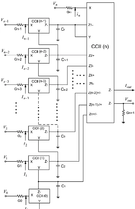
Figure 1 shows the proposed mixed-mode nth-order
universal filter structure where In, In-1, In-2 ,…, I2, I1, I0 are
the filter input currents and Vn, Vn-1, Vn-2 ,…, V2, V1, V0 are
the filter input voltages whose setting determine the filter
functions as shown later, Iout and Vout are the filter current
output and voltage output, respectively. The choice of the
subscript +/- of the output terminal Zn+/- in the CCII(n)
depends on an even/odd order n of the high-order filter,
respectively. Using standard notation, the port relations of a
CCII can be characterized by IY = 0, VX = VY and IZ± = ±
IX. The multiple current outputs of CCII(n) can be simply
reconstructed using current mirrors. Moreover, all current outputs have very high output impedance.
[image:2.612.330.557.163.513.2]Routine circuit analysis for Figure 1 yields the following transfer functions:
Figure 1. Proposed mixed-mode nth-order universal filter structure.
) (
) ( ) (
1D s
G
s N s N V
n i v out
(1)
and
) (
) ( ) (
s D
s N s N
Iout v i (2)
in which
n
i
i i i i i
v s aGVs
N
0
1 )
International Journal of Emerging Technology and Advanced Engineering
Website: www.ijetae.com (ISSN 2250-2459,ISO 9001:2008 Certified Journal, Volume 4, Issue 8, August 2014)
34
n i i i i ii s aIs
N
0 1 )
( (4)
n i i i n s a s D 0 1 )( (5)
where n i i n C a 1 (6) n k j j k i i
k C G
a
1 1
for k1,2,3,...,n1 (7)
n j j G a 1
0 (8)
From equation (1)-(8), the high-order mixed-mode universal filter transfer functions are obtained according to input voltage or current conditions as follows.
Part I: If In = In-1 = In-2 =……= I2 = I1 = I0 = 0, the
following nth-order voltage-mode and
transadmittance-mode filter responses can be obtained as below.
(i) Highpass: Vn = Vin , and all the other input
voltages are zero (grounded).
(ii)Lowpass: V0 = Vin , and all the other input voltages are
zero (grounded).
(iii)bandpass: If n is even, then V(n/2) = Vin , whilst all the
other input voltages are zero (grounded). If n is odd,
then the input current Vin is applied to either V(n-1)/2 or
V(n+1)/2 , whilst all the other input voltages are zero
(grounded).
(iv)Band-reject: Vn = V0 = Vin , and all the other input
voltages are zero (grounded).
(v)All-pass: Vn = Vn-1 = Vn-2 =…= V2 = V1 = V0 = Vin and
Gn = Gn-1 = …= G1 = G0
Part II: If Vn = Vn-1 = Vn-2 =……= V2 = V1 = V0 = 0, the
following nth-order current-mode and
transimpedance-mode filter responses can be obtained as below.
(i) Highpass: In = Iin , and all the other input
currents are zero.
(ii)Lowpass: I0 = Iin , and all the other input currents are
zero.
(iii)bandpass: If n is even, then I(n/2) = Iin , whilst all the
other input currents are zero. If n is odd, then the
input current Iin is applied to either I(n-1)/2 or I(n+1)/2 ,
whilst all the other input currents are zero.
(iv)Band-reject: In = I0 = Iin , and all the other input
currents are zero.
(v) All-pass: In = In-1 = In-2 =…= I2 = I1 = I0 = Iin.
Note that there are no critical component-matching conditions or cancellation constraints in the design except the transconductance/voltage allpass response. Moreover, the structure does not need inverting-type input current signals or double-type amplifier for realizing any filter transfer functions and also does not need to change the
network topology. Observing all of the coefficients in D(s)
(i.e., ai,), because an consists of the product of all n
capacitances,……, an-i consists of the product of n-i
capacitances and i conductances……, and a0 consists of the
product of all n conductances, all filtering parameters
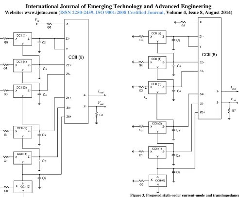
produced from the coefficient in the denominator are orthogonally controllable. In addition to this advantage, the coefficient sensitivity to each capacitance or each conductance is easily calculated and equal to 0 or 1, both of which are low. To illustrate the proposed mixed-mode high-order filter structure, Figure 2 shows a sixth-order transadmittance-mode and voltage-mode highpass filter. Figure 3 shows a sixth-order current-mode and transimpedance-mode bandpass filter. Figure 4 shows a
sixth-order transadmittance-mode and voltage-mode
[image:3.612.49.283.138.342.2]International Journal of Emerging Technology and Advanced Engineering
Website: www.ijetae.com (ISSN 2250-2459,ISO 9001:2008 Certified Journal, Volume 4, Issue 8, August 2014)
[image:4.612.62.554.99.506.2]35
Figure 2. Proposed sixth-order transadmittance-mode and voltage-mode high-pass filter structure.
[image:4.612.53.285.130.511.2]International Journal of Emerging Technology and Advanced Engineering
Website: www.ijetae.com (ISSN 2250-2459,ISO 9001:2008 Certified Journal, Volume 4, Issue 8, August 2014)
36
III. H-SPICE SIMULATIONS
A CMOS implementation of the CCII± is shown in
Figure 5 [21] with the NMOS transistor aspect ratios (W/L=5μm/1μm) and PMOS transistor aspect ratios (W/L=10μm/1μm). Note that the multiple current outputs of CCII applying the realization of current replicas are very simple. To verify the theoretical analysis of the high-order mixed-mode universal filters, the H-SPICE simulations, using the TSMC 0.25μm process for the proposed circuits of Figure 1, were performed with the component values: (i)
R0 = R1 = … = R6 = R7 = 10kΩ, and C1 = C2 = … = C5 = C6
= 5pF for the sixth-order high-pass, low-pass, band-pass, and band-reject filters of the Figure 1, leading to a center
frequency of f0 = 3.183MHz, and (ii) C1 = C2 = C3 = 5pF,
R1 = 20kΩ, R2 = 10kΩ, and R3 = 5kΩ for the third-order
all-pass filter of the Figure 1, leading to a center frequency of
f0 = 3.183MHz. Their supply voltages are VDD =-Vss =
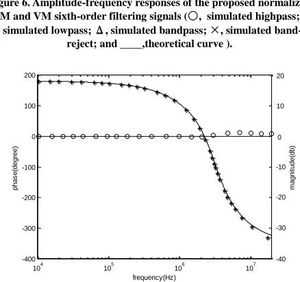
1.25V, Vb1 = -0.3V, and Vb2 = -0.6V. Figure 6 presents
the simulated sixth-order lowpass, bandpass, highpass, and band-reject amplitude-frequency responses of the proposed voltage-mode (VM) and transadmittance-mode (TAM) filters with the normalized transadmittance magnitude = 20
log |10000Iout / Vin| dB due to R7 =10 kΩ. Figure 7 presents
the simulated third-order all-pass phase and amplitude-frequency responses of the proposed current-mode (CM)
and transimpedance-mode (TIM) filters with the
normalized transimpedances magnitude = 20 log |Vout /
10000 Iin| dB due to R7 =10 kΩ. Although not included in
this paper, it can be shown that the other simulated results are very similar to the above simulated results. As can be seen, there is a close agreement between theory and
simulation. Figure 4. Proposed sixth-order transadmittance-mode and
[image:5.612.332.559.120.492.2]International Journal of Emerging Technology and Advanced Engineering
Website: www.ijetae.com (ISSN 2250-2459,ISO 9001:2008 Certified Journal, Volume 4, Issue 8, August 2014)
[image:6.612.64.274.128.463.2]37
Figure 5. CMOS implementation of the CCII±.
106 107
[image:6.612.59.278.471.677.2]-140 -120 -100 -80 -60 -40 -20 0 frequency(Hz) m a g n it u d e (d b )
Figure 6. Amplitude-frequency responses of the proposed normalized TAM and VM sixth-order filtering signals (○, simulated highpass; *
, simulated lowpass; Δ, simulated bandpass; ×, simulated band-reject; and ____,theoretical curve ).
104 105 106 107
-400 -300 -200 -100 0 100 200 frequency(Hz) p h a s e (d e g re e ) 20 10 0 -10 -20 -30 -40 m a g n it u d e (d b )
Figure 7. Phase and amplitude frequency responses of the proposed normalized TIM and CM third-order all-pass signals (*, simulated
phase; ○, simulated amplitude; and ____,theoretical curve).
IV. CONCLUSIONS
Using only n+1 CCIIs, n grounded capacitors, and n+2
resistors, a mixed-mode universal high-order filter is
presented which can realize nth-order lowpass, highpass,
bandpass, band-reject, and allpass responses. Moreover, the proposed high-order circuit offers the following advantages: the minimum active components, using grounded capacitors attractive for integration, high output impedance good for cascadability, no need to change the filter topology, no component-value constraints except the transadmittance/voltage allpass response, no need of inverting or double-type amplifiers for special input signals, and low active and passive sensitivities. As far as active
components is concerned, the proposed nth-order
mixed-mode universal filter using n+1 CCIIs is the minimum
active components. H-Spice simulations confirm the theoretical predictions.
Acknowledgements
The author would like to thank the Ministry of Science and Technology (formerly National Science Council) of Taiwan, R. O. C. The Ministry of Science and Technology, Taiwan, R. O. C. supported this work under grant number NSC 102-2221-E-149-004-.
REFERENCES
[1] C. M. Chang, and B. M. Al-Hashimi, ―Analytical synthesis of current-mode high-order OTA-C filters‖, IEEE Trans. Circuits Syst. I: Fundam. Theory Appl., vol. 50, no. 9, pp. 1188-1192, 2003. [2] C. M. Chang, B. M. Al-Hashimi, Y. Sun, and J. N. Ross, ―New
high-order filter structures using single-ended-input OTAs and grounded capacitors‖, IEEE Trans. Circuits Syst. II: Exp. Briefs, vol. 51, no. 9, pp. 458-463, 2004
[3] C. M. Chang, C. L. Hou, W. Y. Chung, J. W. Horng, and C. K. Tu, ―Analytical synthesis of high-order single-input OTA-grounded C all-pass and band-reject filter structures‖,IEEE Trans. Circuits Syst. I: Regular Papers, vol. 53, no. 3, pp. 489-498, 2006.
[4] C. M. Chang, ―Analytical synthesis of the digitally programmable voltage-mode OTA-C universal biquad‖, IEEE Trans. Circuits Syst. II: Exp. Briefs, vol. 53, no. 8, pp. 607-611, 2006
[5] S. H. Tu, C. M. Chang, N. J. Ross, and M. N. S. Swamy, ―Analytical synthesis of current-mode high-order single-ended-input OTA and equal-capacitor elliptic filter structures with the minimum number of components‖, IEEE Transactions on Circuits and Systems-Part I: Regular Papers, vol. 54, no. 10, pp.2195-2210, 2007.
[6] C. M. Chang, A. M. Soliman, and M.N.S. Swamy, ―Analytical synthesis of low-sensitivity high-order voltage-mode DDCC and FDCCII-grounded R and C all-pass filter structures,‖ IEEE Transactions on Circuits and Systems-Part I: Regular Papers, vol. 54, no. 7, pp. 1430-1443, 2007.
International Journal of Emerging Technology and Advanced Engineering
Website: www.ijetae.com (ISSN 2250-2459,ISO 9001:2008 Certified Journal, Volume 4, Issue 8, August 2014)
38
[8] C. M. Chang, and M. N. S. Swamy, ―Analytical synthesis of odd/even-nth-order elliptic Cauer filter structures using OTRAs‖, International Journal of Circuit Theory and Applications, vol. 41, no. 12, pp. 1248-1271, 2013.
[9] J. W. Horng, ―Analytical synthesis of general high-order voltage/current transfer functions using CCIIs,‖ Microelectronics Journal, vol. 43, no. 8, pp. 546–554, 2012.
[10] C. Acar, ―Nth-order allpass voltage transfer function synthesis using CCII+s: Signal-flow graph,‖ Electronics Letters, vol. 32, no. 8, pp. 727-729, 1996.
[11] C.Acar, ―Nth-order lowpass voltage transfer function synthesis using CCII+s: signal-flow graph approach,‖ Electronics Letters, vol. 32, no. 3, pp. 159-160, 1996.
[12] C. Acar and S. Özoğuz, ―High-order voltage transfer function synthesis using CCII+ based unity gain current amplifiers,‖ Electronics Letters, vol. 32, no. 22, pp. 2030-2031, 1996.
[13] E. Yuce and S. Minaei, ―ICCII-based universal current-mode analog filter employing only grounded passive components,‖ Analog Integrated Circuits and Signal Processing, vol. 58, no. 2, pp. 161-169, 2009.
[14] E. Yuce and S. Minaei, ―On the realization of high-order current-mode filter employing current controlled conveyors,‖ Computers & Electrical Engineering, vol. 34, no. 3, pp. 165-172, 2008.
[15] J. W. Horng, ―High-order current-mode and transimpedance-mode universal filters with multiple-inputs and two-outputs using MOCCIIs,‖ Radioengineering, vol. 18, no. 4, pp. 537–543, 2009. [16] H. A. Alzaher, N. A. Tasadduq, and O. Al-Ees, ―Digitally
programmable high-order current-mode universal filters,‖ Analog Integrated Circuits and Signal Processing, vol. 67, no. 2, pp. 179-187, 2011.
[17] C. N. Lee, ―High-order current-mode universal filter using CCIIs and grounded passive components‖, International Journal of Emerging Technology and Advanced Engineering, vol. 3, no. 8, pp. 608-613, 2013.
[18] C. M. Chang, C. N. Lee, C. L. Hou, J. W. Horng, and C. K. Tu, ―High-order DDCC-based general mixed-mode universal filter‖, IEE Proceedings Circuits, Devices and Systems, vol. 153, no. 5, pp. 511-516, 2006.
[19] C. N. Lee and C. M. Chang, ―High-order mixed-mode OTA-C universal filter‖ AEU-International Journal of Electronics and Communications, vol. 63, no. 6, pp. 517-521, 2009.
[20] C. N. Lee, ―High-order multiple-mode and transadmittance-mode OTA-C universal filters‖, Journal of Circuits Systems and Computers, vol. 21, no. 5, 1250048 (21 pages), 2012.

![Figure 5 [21] with the NMOS transistor aspect ratios = … = R6 = R7 = 10kΩ, and C12C = = … = = = 5pF for the sixth-order high-pass, low-pass, band-pass, and band-reject filters of the Figure 1, leading to a center frequency of f0 = 3.183MHz, and (ii) C1V](https://thumb-us.123doks.com/thumbv2/123dok_us/8709908.881637/5.612.332.559.120.492/figure-transistor-ratios-filters-figure-leading-center-frequency.webp)