CONCLUSION
A new type of stacked meander-chip antenna using LTCC multi-layer technology for dual-band operation with dimensions of 9⫻ 15⫻ 1.2 mm has been proposed. By changing the vertical and horizontal lengths of the meander antenna properly, we can obtain the desired resonant frequency. With the 2.0:1 VSWR impedance bandwidth definition, the lower and upper bands have impedance bandwidths of 80 and 120 MHz, respectively, covering the band-width of the GPS and K-PCS bands. Satisfactory agreement be-tween the simulated and measured results for the antenna patterns
and impedance bandwidth have been achieved. Therefore, the proposed antenna is suitable for practical applications that require a small chip antenna in a mobile-communication system.
REFERENCES
1. K.L. Wong, Planar antennas for wireless communications, Wiley, New York, 2003.
2. S.C. Pan and K.L. Wong, Dual-frequency triangular microstrip antenna with a shorting pin, IEEE Trans Antennas Propagat 45 (1997), 1889 – 1891.
3. C.R. Rowell and R.D. Murch, A compact PIFA suitable for dual-frequency 900/1800-MHz operation, IEEE Trans Antennas Propagat 46 (1998), 596 –598.
4. W.P. Dou and Y.W.M. Chia, Novel meandered planar inverted-F an-tenna for triple-frequency operation, Microwave Opt Technol Lett 27 (2000), 58 – 60.
5. F.R. Hsiao and K.L. Wong, Compact planar inverted-F patch antenna for triple-frequency operation, Microwave Opt Technol Lett 33 (2002), 459 – 462.
6. K.F. Lee, K.M. Luk, K.F. Tong, S.M. Shun, T. Huynh, and R.Q. Lee, Experimental and simulation studies of the coaxially fed U-slot rectan-gular patch antenna, IEE Proc Microwave Antennas Propagat 144 (1997), 354 –358.
© 2005 Wiley Periodicals, Inc.
OPTICAL WIRELESS
COMMUNICATIONS UTILIZING A
DICODE PPM PIN-BJT RECEIVER
M. Menon and R. A. Cryan
Electrical and Electronic Engineering Division School of Engineering and Technology University of Northumbria at Newcastle Newcastle-upon-Tyne, NE1 8ST, UK
Received 28 October 2004
ABSTRACT:Original results are presented for an optical wireless sys-tem employing dicode pulse position modulation (DiPPM) and a PIN-BJT receiver. When operating at⫽0.85m and a bit rate of 10 Mb/s, a sensitivity of⫺51 dBm (Pe⫽10⫺9) is achieved, which repre-sents a 10.3-dB improvement, as compared to an equivalent PCM sys-tem. The work also demonstrates that DiPPM achieves comparable sen-sitivities to those of the digital PPM format, but at significantly reduced line rates, thus making it a credible candidate for mobile devices using optical wireless technology.© 2005 Wiley Periodicals, Inc. Microwave Opt Technol Lett 45: 273–277, 2005; Published online in Wiley Inter-Science (www.interscience.wiley.com). DOI 10.1002/mop.20794
Key words:optical wireless systems; sensitivity performance; dicode PPM; digital PPM
1. INTRODUCTION
[image:1.612.56.296.32.216.2]The application of the digital pulse-position modulation (PPM) format for use in optical wireless communications has been widely studied [1–9] due to its high sensitivity, which is ideal for portable devices, along with its immunity to near-DC noise from fluores-cent lamps. Refluores-cently, Sibley [10, 11] has proposed a related PPM format known as dicode PPM (DiPPM) and demonstrated that it offers advantages over digital PPM. His studies were limited to optical fibre transmission; thus, this paper analyses, for the first time, the DiPPM format for use in optical wireless systems. The performance of a DiPPM system employing a PIN-BJT receiver is analysed in order to determine the system sensitivity. The receiver Figure 5 Simulated and measure return losses of proposed antenna.
[Color figure can be viewed in the online issue, which is available at www.interscience.wiley.com.]
[image:1.612.54.297.412.688.2]configuration employed is the common-collector common-emitter PIN-BJT design, as it offers wide bandwidth and low noise. The sensitivity calculations show that there is an improvement of 0.3 dB between the DiPPM PIN-BJT system and a PPM PIN-BJT system proposed previously by one of the authors [7]. The system is modelled at various values of channel receiver bandwidths (CRBs), DiPPM run-length values, and PPM coding levels. For comparison purposes, both the DiPPM and digital PPM systems are modelled with the same receiver parameters, with receiver bandwidth and noise current values being set to 70 MHz and 7.29⫻10⫺24A2/Hz, respectively. The DiPPM PIN-BJT
config-uration achieved a sensitivity of⫺51 dBm (0.3-dB improvement, compared to⫺50.7 dB achieved by PPM) at a bit rate of 10 Mb/s, commonly used for indoor communication networks. Thus, the original results presented in this paper demonstrate that DiPPM achieves equivalent sensitivities to those for digital PPM, but at significantly reduced line rates and, for the systems considered, the line rate is reduced from 23 times the PCM line rate for digital PPM to four times the PCM line rate for DiPPM.
2. DICODE PPM MODEL AND ERROR SOURCES
The dicode PPM technique is illustrated in Figures 1 and 2. Dicode signalling encompasses data transitions from logic 0 to logic 1 and from logic 1 to logic 0, represented by positive (⫹V) and negative (⫺V) voltages. The positive pulses are known as SET (S), negative pulses as RESET (R), and no pulses (no transition) as NO PULSE (N). Figure 2 shows that when no data transitions are present, there is no pulse, but when transitions occur from 0 to 1 and 1 to 0, there are SET and RESET pulses, respectively. Also, it shows that the information in a single slot in PCM can be coded into a single slot in DiPPM (S or R), which reduces the power requirement of the system. Two guard slots are at the end of each frame to address pulse dispersion and deter interframe interference (IFI).
The sequence in DiPPM is R,xN, S and the probability of a pulse in slot S or slot R is 1/4 while NO PULSE (N) is 1/2. The run length (line coding) is the maximum number of consecutive like symbols (n) allowed in the PCM data stream before the insertion of a pulse to ensure maintenance of timing content. If the maxi-mum DiPPM run is R,nN, S, the probability of S will be one due to the fact that an S symbol will be present at the end of that run.
There are three types of errors in DiPPM; erasure, wrong-slot, and false-alarm errors.
2.1. Erasure Errors
An erasure error of a pulse occurs when the noise level is greater than the pulse signal and this condition “pulls” the peak signal voltage below the threshold level, thus preventing correct detec-tion. The probabilityPris given by
Pr⫽0.5erfc
冉
Qr
冑
2冊
, (1)where
Qr⫽
p⫺d
冑
具n0共t兲2典, (2)
wherepanddare the peak receiver-output voltage occurring at time instanttdand the voltage at the receiver output when crossing the threshold-crossing timetd, respectively. For a DiPPM system, the erasure of a SET or RESET pulse creates the same amount of PCM errors, thus giving the probability
PerDiPPM⫽2
冉
冘
x⫽0n⫺1
冉
1 2冊
x⫹3
Pr共x⫹1兲⫹
冉
1 2冊
n⫹3
Pr共n⫹1兲
冊
, (3)wherenis the maximum number of consecutiveN symbols and
x⫹ 1 is the amount of PCM errors.
2.2. Wrong-Slot Errors
Wrong-slot errors are caused when the rising edge of a detected pulse causes the initial pulse to appear in the adjacent time slots, that is, this particular pulse will produce a threshold-crossing event in either the preceding or the following time slot. The probability of this error is given by
Ps⫽erfc
冉
Qs
冑
2冊
, (4) [image:2.612.74.273.68.248.2] [image:2.612.320.558.458.700.2]where Figure 1 PCM trace corresponding to bits
QS⫽
冉
mTn 2n
冊
2 1
具n0共t兲2典
冉
d0
dt
冏
td冊
2
. (5)
In DiPPM, the wrong-slot error can cause four possible cases. In cases 1 and 2, the pulse is in slot S, which will cause the edge to appear in the preceding or following guard slots, respectively. For cases 3 and 4, when the pulse is in slot R, the edge might appear in the preceding S slot or in the following guard slot, respectively. However, case 1 will not cause any detection error because the decoder will not recognise it as a false threshold crossing, due to the fact that it appears in the preceding guard slot. Since the remaining cases generates the same number of errors, the total PCM error probability can be accumulated as follows:
PewsDiPPM⫽3
冉
冘
x⫽0n⫺1
冉
1 2冊
x⫹3
䡠共x⫹1兲䡠Ps⫹
冉
1 2冊
n⫹3
䡠共n⫹1兲䡠Ps
冊
. (6)2.3. False-Alarm Errors
The false-alarm error can be best described as an unauthorised threshold-crossing event. This is due to the fact that the noise causes a threshold-crossing event in an unoccupied data slot. Thus, the probability is given by
Pt⫽0.5erfc
冉
Qt
冑
2冊
, (7)where
Qt2⫽
d2 具n0共t兲2典
. (8)
The number of uncorrelated samples per time slot can be estimated in terms of the timeRat which the autocorrelation function of the receiver filter has become small, as (mTn/nR). The probability per time slot of a false alarm error is approximated by
Pf⫽
冉
mTn
nR
冊
䡠Pt, (9)
whenPfⰆ1. When the pulse is in slot S, a false alarm can occur in the followingRslot. However, this condition is brought to a halt because the decoder stops when a pulse is received. Therefore, no PCM errors are generated. An error is generated when a false alarm occurs in a string of N (NO PULSE) signals. The severity of the error depends on the location where the false alarm occurs in that particular string. Since the false alarm error occurs on thekth
N symbol in a run ofxN symbols, the PCM error is (x⫹1⫺k). Therefore,
PefDi-PPM⫽2
冘
y⫽1M⫺1
冘
k⫽1
y
冉
1 2冊
y⫹3
Pf共y⫹1⫺k兲
⫹2
冘
k⫽1n
冉
1 2冊
n⫹3
Pf共n⫹1⫺k兲 (10)
and the factor of two denotes the effects of false alarm in slot S is similar to the one in slot R.
3. PIN-BJT RECEIVER AND SYSTEM PERFORMANCE The system configuration for DiPPM consists of a preamplifier (PIN-BJT) followed by a matched filter, threshold detector, and DiPPM decoder, and is similar to the digital PPM system config-uration. In digital PPM, a noise-whitened matched filter and a PDD network are typically used as an optimum receive filter, but if pulse dispersion is low, the PDD is redundant, which is the assumption used in this paper. The receiver employed is a transimpedance PIN-BJT preamplifier based on a self-biasing common-collector common-emitter design [7] that offers wide bandwidth and low noise. The key receiver parameters are a bandwidth of 70 MHz, a photodiode responsitivity of 0.5 A/W, a noise-power spectral density of 7.29⫻10⫺24A2/Hz, and a transimpedance valueR
tof 4.4k⍀. The input pulse shape is assumed to be Gaussian, having the property such that
冕
⫺⬁⬁
hp共t兲dt⫽1 (11)
and, assuming the received pulse shape is normalised, it can then be defined as
hp共t兲⫽ 1
␣
冑
2exp冉
⫺t22␣2
冊
. (12)Thus,
Hp共兲⫽exp
冉
⫺␣22
2
冊
, (13)where the pulse variance ␣ corresponds to the channel-receiver bandwidth (CRB) represented by the following equation:
␣ ⫽0.2Tb
CRB , (14)
whereTbis the PCM bit period andCRBcorresponds to the fact that the DiPPM system consumes the same bandwidth as the PCM system whenCRB⫽1, twice the bandwidth whenCRB⫽2, and so on. The receiver is assumed to have a single-pole response with a⫺3-dB bandwidth of fc, then the current at threshold crossing instant will be given by
i0共t兲⫽
bq
2
冕
⫺⬁
⬁ R
t 1⫹共j/c兲
exp共⫺␣22兲exp共jt兲d
⫽bqRt
c 2 exp共␣
2
c
2兲exp共⫺
ct兲erfc
冉
␣c⫺t
2␣
冊
(15) andd
dti0共t兲⫽bqRt
c2 2 exp共␣
2
c
2兲exp共⫺
ct兲
⫻
冋
exp共⫺共␣c⫺t/ 2␣兲2兲␣c
冑
⫺erfc
冉
␣c⫺t
where b is the number of photons per pulse, is the quantum efficiency, andqis the electron charge. The noise from the output of the filter can be expressed as
具n02典⫽ S0
2
冕
⫺⬁ ⬁
兩Hp共兲Zpre共兲兩2d
⫽S0
c
2 Rt2exp共␣2c2兲erfc共␣c兲, (17) whereS0 is the double-sided input noise-current spectral density [10].
4. RESULTS AND DISCUSSION
The system is designed to operate at an error rate of 10⫺9and a
[image:4.612.318.558.33.203.2]PCM bit rate of 10 Mb/s with a wavelength of 0.85 m. The sensitivities of the PIN-BJT PPM system, assuming a modulation index ofm⫽0.8, and the PIN-BJT DiPPM system are shown in Figures 3 and 4, respectively.
Figure 3 shows the characteristic performance of a digital PPM system in that sensitivity improves with coding level, as the single
[image:4.612.60.291.34.219.2]PPM pulse is being used to conveyM bits of information. This improvement continues until the PPM slots become too narrow and wrong-slot errors begin to occur. Increasing the coding level beyond this point narrows the slots even further, which leads to an increased occurrence of wrong-slot errors and system degradation. Figure 3 shows that the sensitivity of the digital PPM system also improves with CRB, reflecting the fact that high CRB’s leads to narrower pulses and hence less pulse energy.
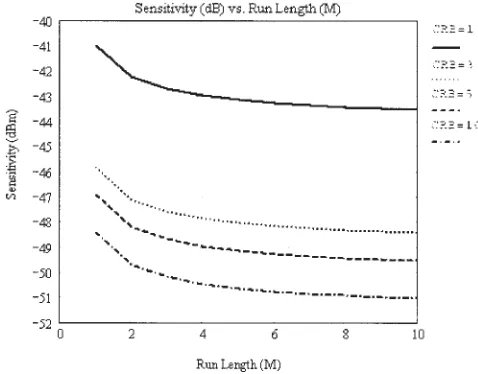
Figure 4 shows the results for the PIN-BJT DiPPM system and demonstrates that the sensitivity improves as the run-length value increases. This is to be expected, since increasing the run length increases the allowable length of the run of dicode zeroes prior to the insertion of a pulse to maintain synchronisation. The PIN-BJT DiPPM system also improves with increased CRB, which again reflects the fact that narrower pulses are being used to convey the information.
Figure 5 shows a comparison of the optimum performances of both systems. For DiPPM, this occurs at a CRB value of 10 and a run length of 10, which gives a sensitivity of⫺51 dBm. For digital PPM, the optimum sensitivity of ⫺50.7 dBm occurs at a CRB value of 10 and a PPM coding level ofM⫽7. This demonstrates that the Dicode PPM system offers a comparable performance to that of digital PPM. However, this is achieved at a significantly reduced line rate in comparison to PCM. In the case of Dicode PPM, the line rate is four times that of the equivalent PCM system; however, for digital PPM it is 23 times (2M
/mM⬇23) the PCM line rate.
In [7], the sensitivity of an equivalent PIN-BJT PCM system operating at 10 Mb/s was evaluated and shown to be⫺40.7 dBm. Therefore, DiPPM offers a sensitivity improvement of 10.3 dB, as compared to the equivalent PCM system, but at a much reduced line rate in comparison to the equivalent digital PPM system.
5. CONCLUSION
Original results have been presented for a PIN-BJT Dicode PPM system operating at a bit rate of 10 Mb/s and employing a receiver with a noise current of 7.29⫻10⫺24A2/Hz and a bandwidth of 70
[image:4.612.53.292.522.709.2]MHz. The sensitivity of the PIN-BJT DiPPM system has been compared to an equivalent PIN-BJT PPM system, demonstrating equivalent performance but at a much reduced line rate. The results also demonstrate a 10.3-dB improvement over a comparable PCM system. The high sensitivity and the low line rate expansion Figure 3 PIN-BJT PPM sensitivity for various CRB values
Figure 4 PIN-BJT DiPPM sensitivity for various CRB values
associated with the DiPPM technique make it an attractive mod-ulation format for indoor infrared wireless transmission.
REFERENCES
1. H.H. Chan, J.M.H. Elmirghani, and R.A. Cryan, An equalization technique for indoor IR wireless LANs, Microwave Opt Technol Lett 10 (1995), 235–238.
2. R.A. Cryan, A.J. Phillips, and J.M. Senior, An improved analysis for optically preamplified pulse-position modulation receivers in optical fibre systems, Microwave Opt Technol Lett 10 (1995), 108 –111. 3. A.J. Phillips, R.A. Cryan, and J.M. Senior, An optically preamplified
digital PPM receiver with improved suboptimum filtering, Microwave Opt Technol Lett 14 (1997), 23–28.
4. D. Chadha and P.K. Rathore, Performance of pulse modulation schemes for infrared wireless communications, Asia-Pacific Micro-wave Conf, 2000, pp. 946 –949.
5. L. Diana and J.M. Kahn, Rate-adaptive modulation techniques for infrared wireless communications, IEEE Int Conf Commun, 1999, pp. 597– 603.
6. P. Djahani and J.M. Kahn, Analysis of infrared wireless links employ-ing multibeam transmitters and imagemploy-ing diversity receivers, IEEE Trans Commun 48 (2000), 2077–2088.
7. J.M.H. Elmirghani, H.H. Chan, and R.A. Cryan, Sensitivity evaluation of optical wireless PPM systems utilising PIN-BJT receivers, IEE Proc Optoelectron 143 (1996), 355–359.
8. J.M.H. Elmirghani and R.A. Cryan, Indoor infrared wireless networks utilising PPM CDMA, Singapore ICCS ’94 Conf Proc 1 (1994), 334 –337.
9. Y.A. Alqudah and M. Kavehrad, Optimum order of angle diversity with equal-gain combining receivers for broadband indoor optical wireless communications, IEEE Trans Vehic Technol 53 (2004), 94 – 105.
10. M.J.N. Sibley, Dicode pulse position modulation: A novel coding scheme for optical-fibre communications, IEE Proc Commun 150 (2003), 125–131.
11. M.J.N. Sibley, Analysis of dicode pulse position modulation using a PINFET receiver and a slightly/highly dispersive optical channel, IEE Proc Optoelectron 150 (2003), 205–209.
© 2005 Wiley Periodicals, Inc.
A MONOLITHIC 5.2-GHz
SINGLE-ENDED INPUT AND SINGLE-SINGLE-ENDED
OUTPUT GaInP/GaAs HBT
UPCONVERSION GILBERT MIXER WITH
INTEGRATED OSCILLATOR
C. C. Meng,1S. K. Hsu,2and G. W. Huang3 1Department of Communication Engineering
National Chiao Tung University Taiwan, R.O.C.
2Department of Electrical Engineering
National Chung-Hsing University Taiwan, R.O.C.
3National Nano Device Laboratories
Taiwan, R.O.C.
Received 16 November 2004
ABSTRACT:A truly balanced operation of a 5.2-GHz Gilbert micro-mixer with a single-ended input and a single-ended output is demon-strated using 2-m GaInP/GaAs HBT technology. Because the micro-mixer has a single-ended input, a passive LC current combiner is used to convert the mixer-differential output into a single-ended output. A cross-coupled LC oscillator with oscillation frequency of 4.3 GHz and a cascode buffer amplifier are also integrated in the same chip. The fully integrated upconversion micromixer has conversion gain of⫺2.5 dB
and OP1dBof⫺12.5 dBm when input IF⫽0.9 GHz and thus output RF⫽5.2 GHz. The IF input return loss is better than 25 dB for fre-quencies up to 6 GHz, while the RF output return loss is better than 12 dB for frequencies from 5.15 to 5.35 GHz.© 2005 Wiley Periodicals, Inc. Microwave Opt Technol Lett 45: 277–279, 2005; Published online in Wiley InterScience (www.interscience.wiley.com). DOI 10.1002/mop. 20795
Key words:GaInP; HBT; mixer; oscillator
1. INTRODUCTION
A monolithic 5.2-GHz upconversion micromixer with an inte-grated oscillator, as shown in Figure 1, is demonstrated in this paper using a 2-m GaInP/GaAs HBT technology. The micro-mixer [1] proposed by Gilbert is the ideal circuit for a micro-mixer at RF frequencies because the intrinsic single-to-differential input stage of a Gilbert micromixer renders a high-speed response and facil-itates wideband impedance matching. A passive LC current com-biner can double the current gain [2– 4] by converting the mixer-differential output into a single-ended output. A cross-coupled LC oscillator with a balanced cross-coupled cascode buffer amplifier is used here to provide balanced signals to the LO port of the mixer. Thus, a truly balanced operation of a Gilbert micromixer with a single-ended input and a single-ended output is achieved at 5.2 GHz.
The fully integrated GaInP/GaAs HBT upconversion micro-mixer demonstrated has a conversion gain of⫺2.5 dB and OP1dB of⫺12.5 dBm when input IF⫽0.9 GHz and thus output RF⫽5.2 GHz. The oscillation frequency of the integrated oscillator is 4.3 GHz. The IF input return loss is better than 25 dB for frequencies up to 6 GHz, while the RF output return loss is better than 12 dB for frequencies from 5.15 GHz to 5.35 GHz. The die size is 1 mm2.
2. CIRCUIT DESIGN
[image:5.612.320.560.550.699.2]The circuit schematic of a GaInP/GaAs downconversion micro-mixer is illustrated in Figure 1 and a photograph of the fabricated circuit is shown in Figure 2. The GaInP/GaAs HBT device has a 35-GHz cutoff frequency. A double-balanced Gilbert mixer has been widely used to implement mixer-integrated circuits due to the excellent port-to-port isolations. However, the common-mode re-jection provided by the biased current source in a conventional Gilbert mixer deteriorates rapidly at high frequencies [5] and degrades the port-to-port isolations. The single-to-differential in-put stage in a micromixer is not only used to turn an unbalanced signal into balanced signals, but also eliminates the need for
![Figure 5Simulated and measure return losses of proposed antenna.[Color figure can be viewed in the online issue, which is available atwww.interscience.wiley.com.]](https://thumb-us.123doks.com/thumbv2/123dok_us/385384.1039046/1.612.54.297.412.688/figure-simulated-measure-proposed-antenna-gure-available-interscience.webp)