Efficient CNFET-based Rectifiers for Nanoelectronics
Mohammad Hossein Moaiyeri
Nanotechnology and Quantum Computing Lab., Shahid Beheshti University, G.C.,
Tehran, Iran
Keivan Navi
Faculty of Electrical and Computing Engineering, Shahid
Beheshti University, G.C., Tehran, Iran
Omid Hashemipour
Faculty of Electrical and Computing Engineering, Shahid
Beheshti University, G.C., Tehran, Iran
ABSTRACT
By scaling down the feature size of CMOS technology deeply in nanoranges, many problems and challenges, such as short channel effects, will restrict its usefulness for the near future robust and energy efficient applications. The CNFET nanodevice seems to be a feasible alternative for bulk CMOS due to its unique electrical properties and similarities with MOSFET. In this paper, efficient CNFET-based analog inverter, half-wave rectifier and full-wave rectifier circuits are proposed for nanoelectronics. The proposed rectifiers are designed based on a CNFET-based 2-transistor analog inverter and a 2-transistor MAX structure. While the previous designs have suffered from a high number of transistors or threshold loss problem, the unique properties of CNFET nanodevice, such as tunable threshold voltage, are utilized in the proposed circuits to reach efficient, full-swing and high-precision designs. The proposed circuits are simulated using HSPICE based on the standard MOSFET-like CNFET model, valid for 10nmtechnology nodes and the functionalities are verified with both DC and transient analyses.
Keywords
Nanoelectronics, Carbon nanotube field effect transistor (CNFET), rectifier, Analog inverter
1.
INTRODUCTION
As the channel length scaled down deeply in nanoranges, different negative effects impressed the current-voltage characteristics of silicon MOSFET family which led to very lower output resistance and device transconductance that restricted the miniaturization of the feature size of this family. Moreover, scaling down the MOSFET technology has resulted in many problems such as reduced gate control, short-channel effects, velocity saturation, carrier mobility degradation, exponentially rising leakage currents [1]. As a result, many emerging nanoscale devices, such as quantum-dot cellular automata (QCA), single electron transistor (SET), Benzene ring FET and carbon nanotube FET (CNFET) have been presented to replace the CMOS technology [2-6]. Considering these nanodevices, CNFET is the most encouraging option for replacing the Si MOSFET in the time to come because of its inherent similarities with conventional MOSFET and the existence of both N-type and P-type transistors, which have led to comparable designing techniques with CMOS technology [6]. In addition, comparing with MOSFET, CNFET is quite faster, consumes lower power and has same electron and hole mobilities (μN=μP) [1,6].
Many applications such as Full Adder cells, MVL circuits, and fuzzy min-max circuits have been designed based on CNFETs [7-9]. However, due to CNFET unique characteristics it can be very useful for designing efficient and high-performance analog circuits.
One of the most widely used analog circuits is voltage rectifier. In general, a rectifier is an electrical circuit that converts an AC signal to a DC signal and the process is called rectification. Rectifiers are generally classified into two types: half-wave rectifier and full-wave rectifier. In half wave rectification of a single-phase supply, one of the positive half or the negative half of the AC input signal is passed and the other half is obstructed. In full wave rectification, both polarities of the input signal are converted to DC.
Classically, rectifiers have widely been used to generate a DC voltage, for use as a source of power, or radio signals detectors [10].
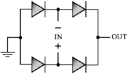
A classical implementation of the rectifier circuit is the well-known four-diode bridge design, shown in Figure 1. However, it is not useful for current on-chip applications. Moreover, the output has 2VD (diode threshold) drop, which makes this
[image:1.595.323.532.407.532.2]design totally unsuitable for current low voltage applications.
Fig 1: The well-known full-wave bridge rectifier
Using Schottky diodes can reduce the diode threshold [11] but 2VD drop is still intolerable. Actually, no DC voltage can be
achieved if VIN < 2VD.
An effective solution based on CMOS technology has been presented in [10] to overcome the output voltage drop. However, in this approach, due to utilizing only PMOS transistors at the output stage, the output does not include voltages smaller than |VthP|, which results in a non-full swing
output and consequently underestimating the average output voltage.
In this work, efficient full-swing rectifier and analog inverter circuits are proposed for low-voltage on-chip applications based on the unique properties of CNFET nano devices.
2.
A REVIEW OF CARBON NANOTUBE
FET (CNFET) AND ITS SPICE MODEL
Carbon Nanotube (CNT) is a carbon allotrope which can be considered as a graphene sheet rolled into a cylindrical nanostructure. CNTs can be categorized into single-walled CNTs (SWCNTs), fabricated of a single tube, and multiwalled CNTs (MWCNTs), fabricated of more than one nested tubes [12]. A vector, called chirality vector, is defined for a CNT, which determines the formation angle of the carbon atoms along the nanotube. The chirality vector is defined by (n1,n2)
pair called chiral number. Many of the physical and electrical properties of a CNT depend on its chirality vector. A SWCNT is metallic if n1-n2=3k (k ) and otherwise it is
semiconducting [12]. The semiconducting SWCNTs can be used as the channel of a CNFET device.
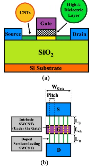
The structure of a typical MOSFET-like CNFET [13-15] is demonstrated in Figure 2.
According to Figure 2(a), the gate width of a CNFET can be calculated based on Equation 1 [13], in which Wmin is the
minimum gate width, determined by lithography, N is the number of nanotubes underneath the gate and Pitch is the distance between the centers of two neighbor CNTs below the same gate.
gate Max( min, )
W W NPitch (1)
Similar to a MOSFET, a CNFET has also a threshold voltage (Vth), which is required for turning on the transistor
electrostatically through the gate. One of the most important and practical characteristics of a CNFET device, which makes it very suitable for designing efficient and high-performance digital and analog circuits, is the capability of determining its threshold voltage by adopting a relevant diameter for its nanotubes. The diameter of the channel CNTs (DCNT) directly
affects the bandgap and consequently the threshold voltage of the CNFET. The threshold voltage of a CNFET is approximately considered to the first order as the half bandgap of its CNTs and is calculated based on the following equation [13]:
bg 0
th
CNT CNT
0.43
2 (nm)
E a V
V
e eD D
(2)
Where, e is the unit electron charge, Ebg is the CNT bandgap,
a0 (0.142 nm) is the carbon to carbon bond length in a CNT
and Vπ (3.033 eV) is the carbon π-π bond energy in the tight
[image:2.595.353.499.79.353.2]bonding model.
Fig 2: Structure of a MOSFET-like CNFET device (a) Cross section view (b) Top view
It can be concluded from Equation 2 that the threshold voltage of a carbon nanotube transistor is inversely proportional to the diameter of its CNTs, which is calculated based on the CNT chiral number (n,m) according to the following equation [13]:
2 2
0 1 1 2 2 2 2
CNT 1 1 2 2
3
0.0783
a n n n n
D n n n n
(3)
For instance, DCNT of a CNFET with the chiral number (n,m)
= (29,0) is 2.27nm and consequently its threshold voltage is 0.192V.
Table 1 Characteristics of the used CNFET SPICE model
Parameter Brief description Value
Lch Physical channel length 10nm
Lss
The length of doped CNT
source-side extension region 10nm
Ldd
The length of doped CNT
drain-side extension region 10nm
Lgeff
The Scattering mean free path in the intrinsic CNT channel and S/D
regions
100nm
Pitch
The distance between the centers of two neighboring CNTs within
the same device
4nm
Leff
The mean free path in p+/n+
doped CNT. 15nm
sub_pitch Sub-lithographic pitch 4nm
Kox
The dielectric constant of high-k top gate dielectric material (HfO2)
16
Tox
The thickness of high-k top gate
dielectric material 4nm
Ksub
The dielectric constant of substrate (SiO2)
4
Csub
The coupling capacitance between the channel region and the
substrate (SiO2)
17aF/μm
Efi The Fermi level of the doped S/D
tube 6eV
phi_M The work function of
Source/Drain metal contact 4.6eV
phi_S CNT work function 4.5eV
3.
THE PROPOSED DESIGNS
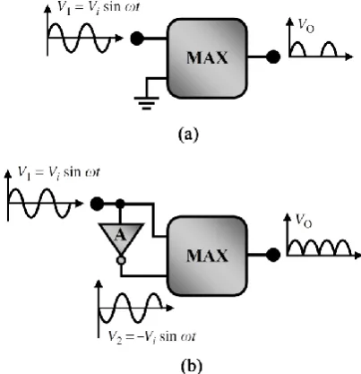
One interesting approach for designing half-wave and full-wave rectifiers is based on analog maximum circuit [16]. As shown in Figure 3(a), for a half wave rectification, a sinusoidal wave (V1ViSint) is fed into the first input of the maximum circuit and the second input is connected to the ground. As a result only the positive cycles of V1 are transferred to output and half-wave rectification
1
1 0
( O )
V
[image:3.595.65.267.527.736.2]V V is obtained.
Fig 3: Designing rectifier circuits based on analog MAX circuit (a) Half-wave rectifier (b) Full-wave rectifier
Furthermore, as demonstrated in Figure 3(b), for a full wave rectification, a sinusoidal signal with 180o phase difference with the first input signal (V2 ViSint) is fed to the second input. The required 180o phase difference can be provided by means of an analog inverter. Accordingly, the half negative and positive cycles of both inputs are overlapped and only positive cycles of V1 and V2 are transferred to the
output and full-wave rectification (
1 2
1 0 2 0
O V V
V V V ) is obtained.
Two key points in implementing this method at transistor level are efficiency of the maximum circuit and rail-to-rail operation of the analog inverter. As the inputs of the MAX circuit for half-wave and full-wave rectifications are specific inputs, a very simpler circuit can be used instead of a complex MAX circuit.
The proposed 16nm CNFET-based half-wave rectifier, composed of only two P-CNFETs, is shown in Figure 4. As in a single P-FET VOUT=Max(VIN,(VG-VthP)), the positive cycles
of the input signal are passed to the output through P1 (P2 is
OFF) and when the input is negative the output remains zero through P2 (P1 is OFF). According to Equation 2, using
CNFETs with large diameters eliminates the voltage drop, leads to a full-swing output and enhances the speed and the driving capability of the circuit. Moreover, by adopting the suitable number of tubes under the gate (N), the desired driving power can be met. In this design, Lch=LS=LD=16nm,
Pitch=20nm, DCNT=3.132nm and N=12.
Fig 4: The proposed CNFET-based half-wave rectifier
The proposed efficient CNFET-based full-wave rectifier, composed of only 4 transistors, is shown in Figure 5. Although a single P-FET has the definition of the maximum function inherently (VOUT=Max (VIN, (Vg-VthP))), the output
voltage is correct only when the gate voltage is less than or equal to the drain voltage. As a result, two P-CNFETs should be used such as shown in Figure 2. Moreover, as a general MAX circuit, in some cases, such as when both inputs are high, the output will be floating. However, this situation does not occur at all due to 180o phase difference between the inputs of the full-wave rectifier. In this situation, at least one of the transistors is ON and passes the correct voltage to the output node. According to Equation 2, using CNFETs with large diameters leads to elimination of the voltage drop problem and improvement of both driving capability and speed of the circuit. In this design for P1 and P2 CNFETs,
Lch=LS=LD=16nm, Pitch=20nm, DCNT=3.132nm and N=12.
In order to provide an 180o phase difference, an analog inverter is proposed which is designed based on the unique properties of the CNFET nanodevice. The proposed analog inverter is composed of two CNFETs indicated with T1 and T2
Fig 5: The proposed CNFET-based full-wave rectifier
The main idea is to modify the behavior of a digital inverter to obtain an analog inverter, by keeping the transistors in saturation condition. This can be achieved by using CNFETs, which have adoptable threshold voltages due to the adjustability of the diameters of their CNTs. The diameter of both N-CNFET and P-CNFET transistors are set to be 4.3nm. Therefore, as shown in Figure 6(a), the Voltage Transfer Characteristic (VTC) curve of the analog inverter is full-swing and quite near ideal with more than 98% accuracy. Figure 6(b) shows the transient response of the proposed analog inverter. In this design for T1 and T2 CNFETs,
Lch=LS=LD=90nm, Pitch=5nm, DCNT=4.3nm and N=15.
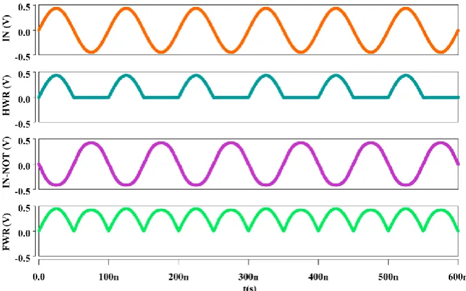
The transient responses of the proposed designs are shown in Figure 7. According to the simulation results the proposed designs operate correctly, with full voltage swing and with high precision. In addition, the delay, average power consumption and energy consumption of the proposed full-wave rectifier are calculated as 4.6ps, 50μW and 230aJ.
4.
Conclusion
This paper presents efficient CNFET-based half-wave and full-wave rectifiers for on-chip nanoelectronics applications. The proposed rectifiers are designed based on analog maximum and inverter circuits. However, for implementing the MAX circuit an efficient 2-transisitor structure is utilized
in the proposed designs. The previous designs have high number of transistors or suffered from Vth loss problem.
However, the unique attributes of CNFET nanodevice, such as adjustable Vth, are utilized in the proposed circuits to obtain
[image:4.595.75.257.68.218.2]full-swing, efficient and high-precision designs. The proposed circuits are simulated using HSPICE based on the standard MOSFET-like CNFET model, valid for 10nm nodes and their operations are verified with both DC and transient analyses.
Fig 6: Functionality of the proposed analog inverter (a) DC response (b) Transient response
[image:4.595.341.512.179.482.2] [image:4.595.128.466.521.732.2]5.
ACKNOWLEDGMENTS
This work has been supported by the Grant number 600/629 from the vice presidency of research and technology of Shahid Beheshti University, G. C.
6.
REFERENCES
[1] Kim Y.-B., "Challenges for Nanoscale MOSFETs and Emerging Nanoelectronics," Transactions on Electrical and Electronic Materials, Vol. 11, No. 3, pp. 93-105, 2010.
[2] Sayedsalehi S., Moaiyeri M. H., Navi K., "Novel Efficient Adder Circuits for Quantum-Dot Cellular Automata," Journal of Computational and Theoretical Nanoscience, Vol. 8, No. 9, pp. 1769-1775, 2011.
[3] Navi K., Tehrani M. A., Khatami M., "Well-Polarized Quantum-dot Cellular Automata Inverters," International Journal of Computer Applications, Vol. 58, No. 20, pp. 10-13, 2012
[4] Sahafi A., Moaiyeri M. H., Navi K., Hashemipour O., "Efficient Single-Electron Transistor Inverter-Based Logic Circuits and Memory Elements," Journal of Computational and Theoretical Nanoscience, Vol. 10, 2013.
[5] Ghasemi M., Sam M., Moaiyeri M. H., Khosravi F., Navi K., "A new SPICE model for organic molecular transistors and a novel hybrid architecture," IEICE Electronics Express, Vol. 9, No. 10, pp. 926-931, 2012.
[6] Moaiyeri M. H., Doostaregan A., Navi K., "Design of Energy-Efficient and Robust Ternary Circuits for Nanotechnology," IET Circuits, Devices & Systems, Vol. 5, No. 4, pp. 285–296, 2011.
[7] Lin S., Kim Y-B., Lombardi F., "CNTFET-Based Design of Ternary Logic Gates and Arithmetic Circuits," IEEE Transactions on Nanotechnology, Vol. 10, No. 2, pp. 217-225, 2011.
[8] Moaiyeri M. H., Faghih Mirzaee R., Navi K., Momeni A., "Design and analysis of a high-performance
CNFET-based Full Adder,” Taylor and Francis, International Journal of Electronics, Vol. 99, No. 1, pp. 113-130, 2012.
[9] Moaiyeri M. H., Chavoshisani R., Jalali A., Navi K., Hashemipour O., "High-performance Mixed-Mode Universal Min-Max Circuits for Nanotechnology, " Circuits, Systems, and Signal Processing, Vol. 31, No. 2, pp. 465-488, 2012.
[10]Facen A., Boni A., "Power Supply Generation in CMOS passive UHF RFID tags," IEEE research in micro-electronics and micro-electronics, pp. 33-36, 2006.
[11]Karthaus U., Fischer M., "Fully integrated passive UHF RFID transponder IC with 16.7-uW minimum RF input power," IEEE Journal of Solid-State Circuits, Vol. 38, No. 10, pp. 1602-1608, 2003.
[12]McEuen P. L., Fuhrer M., Park H., "Single-Walled Carbon Nanotube Electronics," IEEE Transactions on Nanotechnology, Vol. 1, No. 1, pp. 78-85, 2002.
[13]Deng J., "Device modeling and circuit performance evaluation for nanoscale devices: silicon technology beyond 45 nm node and carbon nanotube field effect transistors,” Doctoral Thesis, Stanford University, 2007.
[14]Deng J., Wong H.-S.P., "A Compact SPICE Model for Carbon-Nanotube Field-Effect Transistors Including Nonidealities and Its Application—Part I: Model of the Intrinsic Channel Region,” IEEE Transactions on Electron Device, Vol. 54, No. 12, pp. 3186-3194, 2007.
[15]Deng J., Wong H.-S.P., "A Compact SPICE Model for Carbon-Nanotube Field-Effect Transistors Including Nonidealities and Its Application—Part II: Full Device Model and Circuit Performance Benchmarking,” IEEE Transactions on Electron Device, Vol. 54, No. 12, pp. 3195-3205, 2007.