FPGA Implementation of Low Power Hardware Efficient
Flagged Binary Coded Decimal Adder
K.N.Vijeyakumar
V.Sumathy
Assistant Professor, Ece, Assistant Professor, Ece,
Anna University Of Technology,
Government College Of Technology, Coimbatore, Coimbatore - 641047. Thadagam Road, Coimbatore-641013.
A.Dinesh Babu, S.Elango, S.Saravanakumar
Pg Scholars, Ece,
Anna University Of Technology Coimbatore,
Jothipuram, Coimbatore - 641047.
ABSTRACT
This paper presents a novel architecture for hardware efficient binary represented decimal addition. We extend the two operand ripple carry addition by one with the third input being constant. The addition technique is made fast by generating flag bits appropriate to the constant added. The third constant in case of our proposed design is 6(0110) for converting the outputs exceeding 9 to Binary Coded Decimal (BCD) number. The proposed BCD adder has been designed using VHDL code and synthesized using Altera Quartus II. Experimental results show that the proposed design outperforms the previous researches in terms of power dissipation and area.
Key Words
Flagged binary adder, Carry look ahead adder, Carry skip adder, Correction circuit, flag bit computation.
1.
INTRODUCTION AND RELATED
WORK
The binary numbering system is, by far, the most common numbering system in use in computer systems today. In days long, however, there were computer systems that were based on the decimal (base 10) numbering system rather than the binary numbering system. Such computer systems were very popular in systems targeted for business/commercial systems. Although systems designers have discovered that binary arithmetic is almost always better than decimal arithmetic for general calculations, the myth still persists that decimal arithmetic is better for money calculations than binary arithmetic. Therefore, many software systems still specify the use of decimal arithmetic in their calculations [16].
BCD representation does offer one big advantage over binary representation: it is fairly trivial to convert between the string representation of a decimal number and its BCD representation. This feature is particularly beneficial when working with fractional values since fixed and floating point binary representations cannot exactly represent many commonly used values between zero and one (e.g., 1/10). Therefore, BCD operations can be efficient when reading from a BCD device, doing a simple arithmetic operation (e.g., a single addition) and then writing the BCD value to some other device. Many architectures and algorithms have been proposed to date for decimal arithmetic. Behrooz shirazi et al., [2] designed an adder for redundant BCD addition. Though the design involves simple conversion of a BCD number to
redundant BCD and perform addition in redundant form and again convert the result back to BCD form, it suffers from high delay .In addition the conversion circuitry used adds to the design complexity. Algorithms and adders for BCD addition are presented in [3] by Robert D.Kenny et al., in which the design using speculative addition technique have regular structure and their correction unit is independent of the number of input operands whereas the other design using non-speculative addition have lower delays.
The use of reversible logic for the design of BCD adders were presented in [4][6][17]. The reversible logic adders perform well in terms of power dissipation and logic count, however it is prone to higher delay. In a pioneer work on BCD addition Sreehari Veeramachaneni et al.,[7] used multiplexer for the addition of correction bits. The circuit has lower delay compared to the architectures using adders for correction bit addition.
Alp Arslan Bayrakci et al.,[8] proposed a BCD adder with efficient carry generation using analyzer circuit. The circuit performs well in terms of delay compared to architectures mentioned in literature and shows better area performance. Anshwal Singh et al.,[9] designed a novel architecture for BCD addition and subtraction . The design uses three major blocks viz., PG block, prefix block and the correction block and generates carry without any extra logic thus performing better in terms of area performance compared to the BCD adder in [10].
Sundaresan.C et al., [11] in a pioneer work on design of Reduced delay BCD adder used Carry Look Ahead (CLA) adder in the initial stage being followed by carry network and correction logic in the second and third stages. Though the circuit is fast compared to the architecture in [12], the use of CLA adder in initial stage increases area cost. Chetan Kumar et al., [12] presented a unified architecture for BCD and binary addition. Though the circuit has lower delay compared to the architectures mentioned in literature the design of post correction circuitry poses problems for multi-bit operands. Osama Al-khaleel et al., [13] proposed a correction free BCD adder in which the input operands are split and added in two stages. Stage 1 adds the MSB three bits of a four bit BCD number and the result out of stage 1 is passed to stage 2 and added with the LSB. The latency of the architecture is very less compared to the architectures mentioned in literature.
stage and flagged computation block are passed through a multiplexer. The control signal for the multiplexer is generated from a control circuit which produces 1 for sum values exceeding 9 and 0 else. The rest of the paper is organized as follows. Section 2 gives a brief description of BCD addition and the architecture of conventional BCD adder. Section 3 discusses about the design of proposed flagged BCD adder. In section 4 the performance of the proposed BCD adder are discussed and compared with the previous approaches. Section 5 gives brief conclusion of the work done.
2. OVERVIEW OF BCD ADDITION
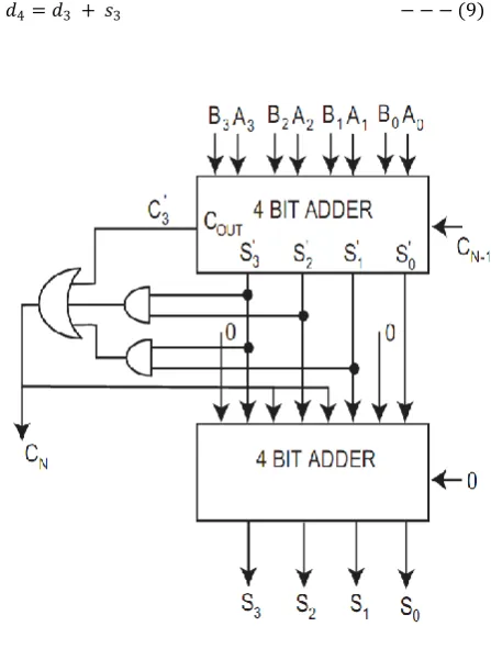
In electronic systems, BCD is an encoding for decimal numbers in which each digit is represented by its own binary sequence. It allows easy conversion to digits and results in faster calculations. When BCD numbers are added, each sum digit should be adjusted to skip the six unused codes. For instance, the addition of two decimal digits in BCD, together with a possible carry from a previous least significant pair of digits (assuming maximum value for input digits) viz., 9 + 9 +1 would result in 19 .The equivalent binary sum will be in the range 0 to 19 represented in binary as 0000 to 10011and BCD as 0000 to 1 1001(the first 1 being carry and next four bits being BCD digit sum). For the binary sum equal to or less than 1001 the corresponding BCD digit is correct. However when the binary sum exceeds 1001, the result is invalid BCD digit. The addition of 6(0110)2 to the binary sum converts it to the correct digit and also produces carry [14]. Fig.1 shows the block diagram of a 1 digit BCD adder [14] based on the above methodology.
The input digits in binary are A3A2A1A0 and B3B2B1B0. S3’ S2’S1’S0’are the outputs of the first stage 4 bit adder, to which correction bits 0110(6) is added at the second stage to produce the BCD number S3S2S1S0 shown in equation (2)-(5)along with carry output CN shown in equation(1).The carry CN will be one for digits exceeding 9 or else it will be 0.
𝐶𝑁= 𝐶𝑂𝑈𝑇 + 𝑆3′𝑆2′ + 𝑆3′𝑆2′ − − − 1
𝑆0= 𝐵0 − − − (2)
𝑆1= 𝐵3′𝐵1+ 𝐵3𝐵2𝐵1 − − − (3)
𝑆2= 𝐵3′𝐵2+ 𝐵2𝐵1 − − − (4)
𝑆3= 𝐵3𝐵2′𝐵1′ − − − (5)
3. PROPOSED FLAGGED BCD ADDER
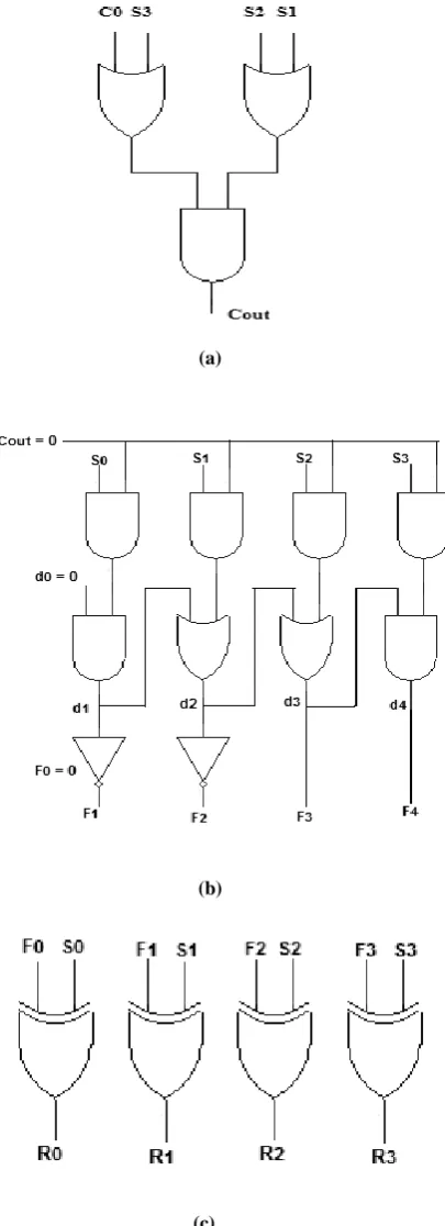
We have proposed a hardware efficient BCD adder using flagged binary addition [1] technique proposed by Vibhuti Dave et al., . The various blocks of the proposed BCD adder are 4 bit Ripple Carry Adder(RCA), Excess 9 detector, flag bit computation block, flag inversion block and four 2:1 multiplexers whose schematic is shown in figure 3.
The input A (a3a2a1a0) and B(b3b2b1b0) are fed to the first stage binary adder.
The sum outputS(S3S2S1S0) and carry out Co of this stage is fed to Excess 9 detector shown in figure 3(a). If the sum S(S3S2S1S0) is less than or equal to 9 the Cout of Excess 9 detector will be zero and the sum S(S3S2S1S0) will be passed out through the multiplexer. If the sum S(S3S2S1S0) exceeds 9, the Coutof Excess 9 detector will be 1 and the sum bits will be passed through the flag bit computation block to generate intermediate carry bits (d4d3d2d1) shown in equation (6)-(9). 𝑑1= 𝑑0 & 𝑠0 − − − (6)𝑑2= 𝑑1 + 𝑠1 − − − (7)
𝑑3= 𝑑2 + 𝑠2 − − − (8)
𝑑4= 𝑑3 + 𝑠3 − − − (9)
[image:2.595.310.547.59.725.2]
Fig.1 Block Diagram of BCD Adder
[image:2.595.315.539.73.369.2]
(a)
(b)
[image:3.595.74.277.71.630.2]
(c)
Fig 3. Schematic of (a) Excess-9 Detector, (b)Carry computation and Flag bit computation block (c) Flag inversion logic
The carry bits(d4d3d2d1) and sum S(S3S2S1S0) are then used by this
block to generate flag bits (F0,F1,F2,F3) shown in equation (10) -(13).
𝐹1= 𝑑1 − − − (10)
𝐹2= 𝑑2 − − − (11)
𝐹3= 𝑑3 − − − (12)
𝐹4= 𝑑4 − − − (13)
The flag bits(F0,F1,F2,F3) and sum S(S3S2S1S0) are passed through
flag inversion logic shown in fig.3(c) to generate the BCD output M3M2M1M0 for S(CoS3S2S1S0)which exceeds 9. The M3M2M1M0 of
the flagged inversion block forms the other input to the multiplexer which is passed out for 1 value of Cout. The pseudo
code for the proposed BCD adder is shown in figure.4.
Fig 4. Pseudo code for proposed flagged BCD adder
4. RESULTS AND DISCUSSION
[image:3.595.320.556.163.553.2]Table 1.Comparison of area, delay and power dissipation of proposed BCD Adder and state-of the art designs.
BCD Adder Area
(No. of Logic Elements)
Delay (ns)
Total thermal power dissipation
(mW)
Core dynamic thermal power dissipation
(mW)
I/O thermal power dissipation
(mW)
Conventional [14]
24 18.415 172 2.82 89.05
Correction free [13]
58 16.326 173.06 3.59 89.34
Carry skip [15]
32 21.123 174.27 2.57 91.56
Proposed-Using
CSLA 25 15.650 175.39 2.55 80.14
Proposed-Using CSA
21 16.494 169.22 2.27 86.83
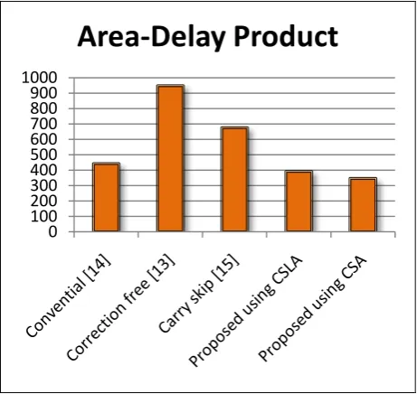
which is2 OR and 1 OR excess of 4 xor delays in CSA based BCD adder[15] and Conventional BCD adder [14] respectively. The Area-Delay-Product (ADP) of the proposed design fair better compared to the previous designs as seen from figure 5. In addition our proposed BCD adders using carry skip addition for the initial stage demonstrates better power dissipation performance compared to the state-of the art designs
.
Fig 5. Graphical representation of Area-Delay-Product
5. CONCLUSION
We have proposed a new BCD adder design by using the concept of high speed addition for three operands (two input operand and a constant) by generating flag bits. Extensive comparison using synthesis results shows that the proposed flagged BCD adder outperformed all other previous designs in terms of power dissipation and area. The potential benefits of reduced logic cell count of our proposed flagged BCD adder can be realized in fair ADP performance. This suggests the suitability of our proposed flagged BCD adder for portable VLSI implementation. Moreover, the proposed BCD adder can be easily extended to multi digit addition.
6. REFERENCES
[1] Vibhuti Dave, Erdal Oruklu and Jafar Saniie,“Constant addition with flagged binary adder arhitectures”, Integration the VLSI journal Vol.43 pp. 258–267 2010.
[2] Behrooz Shirazi, David Y.Y.Yun , and Chang
N.Zhang,“Vlsi Designs for Redundant Binary-Coded Decimal Addition”, IEEE pp.52-56 1988.
[3] Robert D. Kenney and Michael J. Schulte, High-Speed Multi-operand Decimal Adders”, IEEE Transactions On Computers, Vol.54, No.8, pp.953-963, August 2005.
[4] Hafiz Mohammed Hasan Babu and Ahsan Raja Chowdhury, “Design of a Reversible Binary Coded Decimal Adder by Using Reversible 4-bit Parallel Adder”, IEEE, VLSID 2005.
[5] Himanshu Thapliyal and Nagarajan Ranganathan, “A
New Reversible Design of BCD Adder” EDAA 2011.
[6] Ashis Kumer Biswas, Md. Mahmudul Hasan, Moshaddek
Hasan, Ahsan Raja Chowdhury and Hafi Md. Hasan
Babu, “A Novel Approach to Design BCD Adder an carry
Skip BCD Adder” 21st International Conference on VLSI
Design pp. 566-571 2008.
[7]
Sreehari Veeramachaneni, M.Kirthi Krishna,
Lingamneni Avinash, Sreekanth Reddy P,M.B.Srinivas,
“Novel, High-Speed 16-Digit BCD Adders Conforming
to IEEE 754r Format” IEEE Computer Society Annual
Symposium on VLSI (ISVLSI'07), 2007.
[8] Alp Arslan Bayrakci and Ahmet Akkas, “Reduced Delay BCD Adder”, IEEE pp.266-271, 2007.
[9] Anshul Singh, Aman Gupta, Sreehari Veeramachaneni
and M.B. Srinivas, “ A High Performance Unified BCD and Binary Adder / Subtractor”, IEEE Computer Society Annual Symposium on VLSI, pp.211-216 2009.
0 100 200 300 400 500 600 700 800 900 1000
[image:4.595.54.285.370.588.2][10] Sreehari Veeramachaneni.M, Kirthi Krishna.V, Prateek G.S, Subroto.S, Bharat, M.B.Srinivas, “A Novel Carry- Look Ahead Approach to a Unified BCD and Binary Adder/Subtractor”, 21st International Conference on VLSI Design 2008, pages 547-552, January 2008.
[11] SundaresanC, Chaitanya CVS, PR Venkateswaran, Somashekara Bhat and Mohan Kumar J, “Modified Reduced Delay BCD Adder” IEEE4th International Conference on Biomedical Engineering and Informatics (BMEI) 2011, pages 2148-2151.
[12] Chetan Kumar V, Sai Phaneendra P, Syed Ershad Ahmed, Sreehari Veeramachaneni, N, M.B Srinivas,“A
Unified Architecture for BCD and Binary
Adder/Subtractor” , 14th Euromicro Conference on
Digital System Design pp.426-429 2011.
[13] Osama Khaleel, Mohammad Khaleel, Zakaria Al-Qudah,Christos A. Papachristou and Khaldoon Mhaidat, and Francis G. Wolff,” Fast Binary/Decimal Adder / Subtractor with a Novel Correction-Free BCD Addition” IEEE pp.455-459 2011.
[14] Moris Mano - Digital design 3rd edition Prentice Hall
Puclication 2001.
[15] Himanshu Thapliyal, Saurabh Kotiyal and M.B Srinivas, “Novel BCD Adders and their Reversible Logic Implementation for IEEE 754r Format”, Proceedings of the 19th International Conference on VLSI Design (VLSID’06) 2006.
[16] http:// webster.cs.ucr.edu / AoA / Windows / HTML / Advanced Arithmetica6.html – Chapter 4 More data representation – subsection 4.3 - Basics of Binary Coded Decimal (BCD) Representation
[17] B. Ramkumar and Harish M Kittur “Low-Power and Area-Efficient Carry Select Adder”, IEEE transactions on Very Large Scale Integration (VLSI) systems, Vol. 20, No. 2, pp.371-375, February 2012.