Technology (IJRASET)
Design and Implementation Various Logic Circuits
Using GDI Technique
1
N.Naresh,2M.Srinivasulu
1
M.Tech Student, 2Assistant Professor,Department of ECE
Swetha Institute of Technology & Science, Tirupathi, India
Abstract-Area and power are the 2 very important problems in analog circuit style and synthesis of VLSI circuits that depends on varied vital style parameters. The aim of this paper is to style varied logic gates, Comparator and different basic logic circuits victimization space optimizing techniques like complementary & Gate-Diffusion-input (GDI).Mainly the paper contains Full adder, half subtractor, Comparator and different logic gates. This work evaluates and compares the performance and optimized space of mentioned gates with Static CMOS technique and GDI technique victimization completely different levels in Hspice. The schematics area unit enforced in micro wind and logic operation and verification done in Hspice CMOS technology. At first, victimization Hspice Tool, the circuits area unit enforced with Static CMOS technology so with GDI techniques. Simulations results validate the planned idea and verify that GDI technique decreases the world employed by completely different logic circuits.
Keywords: VLSI, GDI, CMOS, Low Power, Power Dissipation, Optimized ALU.
I. INTRODUCTION
Full Adder Cell plays an important role in Digital Signal Processors (DSPs); Application Specific ICs (ASICs), Digital Processors etc., increasing the performance of 1-bit full adder shows a good impact on increasing the performance of the total system. Thus the conclusion of full adders with low power and high performance is incredibly essential. VLSI designers have used speed because the performance metric. In general, tiny space and high performance area unit 2 conflicting constraints. The ability consumed for any given perform in CMOS circuit should be reduced for either of the 2 totally different reasons: one in every of these reasons are to cut back chilling so as to permit an oversized density of functions to be incorporated on an IC chip. Any quantity of power dissipation is worth it as long because it doesn’t degrade overall circuit performance. The opposite reason is to save lots of energy in battery operated instruments same as Electronic watches wherever average power is in microwatts. In CMOS circuits, the ability consumption is proportional to switch activity, electrical phenomenon loading and therefore the sq. of the availability voltage. Full Adder is one in every of the foremost necessary elements of every processor, that is employed in floating-point, within the arithmetic logic unit (ALU), digital signal process, image, video process, and microprocessors and altogether the arithmetic operations like division, multiplication, subtraction. Increasing the performance of a 1-bit Full Adder cell is incredibly effective in increasing the Performance of the total system.
II. COMPONENTS DESIGN WITH COMPLEMENTARY LOGIC
The various components are designed using complementary logic (CMOS logic). Figure shows the schematic design of various components such as ADDER, SUBTRACTOR, LOGICAL GATES (AND,OR,EX-OR).
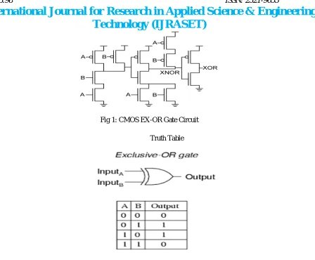
A. CMOS EX-OR Gate
Technology (IJRASET)
Fig 1: CMOS EX-OR Gate Circuit
Truth Table
B. AND Gate Using CMOS Logic
A Logic gate could be a form of digital computer circuit that has AN output that is often at logic level “0” and solely goes “HIGH” to a logic level “1” once its entire inputs area unit at logic level “1”. The output state of a “Logic AND Gate” solely returns “LOW” once more once ANY of its inputs area unit at a logic level “0”. In different words for a logic gate, any LOW input can provides a LOW output.
[image:3.612.155.559.474.657.2]Truth Table
Fig 2: 2-input AND gate using CMOS logic
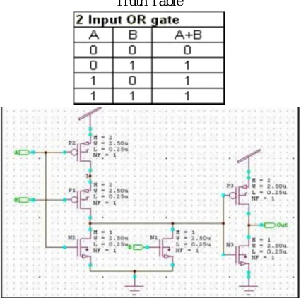
C. OR Gate Using CMOS Logic
Technology (IJRASET)
the alphabet of a “Logic OR Gate” solely returns “LOW” once more once its entire inputs area unit at a logic level “0”. In different words for a logic OR circuit, any “HIGH” input can provides a “HIGH”, logic level “1” output.
[image:4.612.201.414.118.329.2]Truth Table
Fig 3: 2-input OR gate using CMOS logic
D. CMOS Full Adder
Schematic image for a 1-bit full adder with Cin and Cout drawn on sides of block to stress their use in an exceedingly multi-bit adder. A full adder adds binary numbers and accounts for values carried in still as out. A one-bit full adder adds 3 one-bit numbers, typically written as A, B, and Cin; A and B area unit the operands, and Cin could be a bit carried in from the previous lesser stage. The total adder is sometimes an element in an exceedingly cascade of adders, that add eight, 16, 32, etc. bit binary numbers. The circuit produces a two-bit output, output carry and total generally described by the signals Cout and S. The one-bit full adder's truth table is
Truth Table
From the on top of truth-table, the total adder logic will be enforced. We will see that the output S is AN EXOR between the input A and therefore the half-adder total output with B and CIN inputs. We have a tendency to should additionally note that the COUT can solely be true if any of the 2 inputs out of the 3 area unit HIGH. Thus, we will implement a full adder circuit with the assistance of 2
half adder circuits. The primary can half adder are going to be wont to add A and B to provide a partial total. The {second 0.5|last half} adder logic will be wont to add CIN to the total created by the primary half adder to urge the ultimate S output. If any of the 0.5 adder logic produces a carry, there'll be AN output carry. Thus, COUT is going to be AN OR performs of the half-adder Carry
Technology (IJRASET)
Full Adder Circuit using Logic Gates
Though the implementation of larger logic diagrams is feasible with the on top of full adder logic an easier image is generally wont to represent the operation. Given below could be a less complicated schematic illustration of a one-bit full adder.
Fig 4: Logic Diagram & CMOS Full Adder Circuit
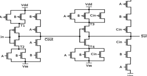
E. CMOS Half Subtractor
[image:5.612.189.424.206.327.2]The Half Subtractor could be a combinatory circuit that's wont to perform the subtraction of 2 bits. It consists of 2 inputs referred to as the number and therefore the number and 2 outputs referred to as distinction and borrow. The number is denoted by input A, the number is denoted by input and therefore the 2 outputs area unit denoted by D and B (Difference & Borrow) severally. The multidimensional language and CMOS Half Subtractor is shown in Fig. 5
Fig 5: Half Subtractor Circuit Using Logic Gates Truth Table
III. GDI METHOD AND COMPONENTS DESIGN
Technology (IJRASET)
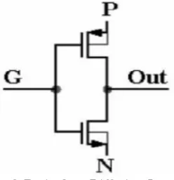
[image:6.612.239.363.271.399.2]permits reducing power consumption, propagation delay, and space of digital circuits whereas maintaining low complexness of logic style. Performance comparison with ancient CMOS and numerous pass-transistor logic style techniques is conferred. The various ways area unit compared with regard to the layout space, variety of devices, delay, and power dissipation. Problems like technology compatibility, top-down style, and pre computing synthesis area unit mentioned, showing benefits and disadvantages of GDI compared to different ways. Many logic circuits are enforced in numerous style designs. Gate Diffusion Input Technique could be a new technique to cut back propagation delay, space and power dissipation. The simplest methodology to style low power digital combinatory circuits is GDI Technique. GDI technique is largely 2 semiconductor unit implementation of advanced logic functions that provides in-cell swing restoration beneath bound operational conditions. The main feature of GDI cell is that the VDD supply won't hook up with the supply of PMOS junction transistor electronic transistor semiconductor device semiconductor unit semiconductor} and therefore the GND won't hook up with the supply of NMOS transistor. Within the place of VDD and GND pins input signals area unit wont to build additional versatile than CMOS style. Figure 6 shows the fundamental GDI cell. The figure 6 explains that there are unit 3 inputs in an exceedingly Basic GDI cell. G (common gate input to NMOS and PMOS), p (input to the source/drain of PMOS) and N (input to the source/drain of NMOS). Table shows the various logic functions enforced with less power consumption and less propagation delay compared to different style techniques.
Fig.6. Basic Gate-Diffusion-Input cell
[image:6.612.201.411.555.627.2]The Gate-Diffusion-Input (GDI) methodology relies on the employment of a straightforward cell as shown in Fig. 13. One could also be think about the CMOS electrical converter within the 1st look of this circuit, however there area unit some major variations within the two: (1) The GDI cell contains 3 inputs G (common gate input of NMOS and PMOS), P (input to the source/drain of PMOS), and N (input to the source/drain of NMOS). (2) Bulks of each NMOS and PMOS area unit connected to N or P (respectively), thus it will be haphazardly biased in distinction to CMOS electrical converter. The fundamental GDI cell is shown in Fig.6. The GDI cell with four ports will be recognized as a replacement Multi-functional device, which may attain six functions with simply totally different combos of inputs G, P and N. TABLE 1. Shows that straightforward configuration changes within the inputs G, P, and N of the fundamental GDI cell will result in terribly totally different Boolean functions at the output out. Most of those functions area unit advanced (usually consume 6-12 transistors) in CMOS, whereas terribly straightforward (only two transistors per function) within the GDI style methodology. Meanwhile, multiple-input gates will be enforced by combining many GDI cells.
TABLE I- Functions of the basic GDI cell Advantages of GDI over CMOS Technology
1. Low power circuit style
2. Permits reducing power consumption. 3. Reducing propagation delay.
Technology (IJRASET)
A. XOR Gate Using GDI cell
The X-OR circuit created with the assistance of GDI cell is AN application of the GDI technique. Because it will be seen in Fig.7, the XOR created exploitation GDI technique needs solely four transistors (2PMOS & 2NMOS). GDI X-OR circuit use less transistors compared with the traditional CMOS XOR.
Fig.7. XOR using GDI cell
B. AND Gate Using GDI Cell
The gate created with the assistance of GDI cell is AN application of the GDI technique. because it will be seen in Fig. 8, the AND created exploitation GDI technique needs solely 2 transistors (1PMOS & 1NMOS).GDI gate use less transistors compared with the traditional CMOS AND.
Fig.8. AND using GDI cell
C. OR Gate Using GDI Cell
The OR circuit created with the assistance of GDI cell is AN application of the GDI technique. Because it will be seen in Fig.9, the OR created exploitation GDI technique needs solely 2transistors (1PMOS & 1NMOS). GDI OR circuit use less transistors compared with the traditional CMOS OR.
Fig.9. OR using GDI cell
D. Half Subtractor Using GDI Cell
Technology (IJRASET)
in Fig.10, the HALF SUBTRACTOR created exploitation GDI technique needs solely eight transistors (4PMOS & 4NMOS).GDI HALF SUBTRACTOR gate use less transistors compared with the traditional CMOS HALF SUBTRACTOR.
Fig.10. Half Subtractor using GDI cell
E. Full Adder Using GDI Cell
The FULL ADDER created with the assistance of GDI cell is AN application of the GDI technique. Because it will be seen in Fig.11, the total ADDER created exploitation GDI technique needs solely eight transistors (4PMOS & 4NMOS).GDI FULL ADDER gate use less transistors compared with the traditional CMOS FULL ADDER.
Fig.11. Full Adder using GDI cell
IV. RESULT
As the range of semiconductor is reduced in the GDI technique ALU it is obvious that its space is optimized. A part from this optimized space of ALU the different evident advantage we tend to get is speed. Apparently because the range of semiconductor used is reduced the operational time is conjointly reduced and operation square measure done in less time. Therefore our new ALU is conjointly quick in operation as compare to its counterpart. Also due to some engaging options that enable enhancements in style complexness, semiconductor counts, static power dissipation and logic level swing, analysis on GDI is changing into feverish in VLSI space. However, the GDI theme suffers the defect of special CMOS method, specifically, it needs twin well CMOS or atomic number 14 on stuff (SOI) method, that square measure a lot of costly than the customary p-well CMOS process[4,9].Similarly with bound modification the subtractor circuit will be created that once more can use less semiconductor than its CMOS counterpart. Same is the case with every gate’s and different component’s circuit. Each style created with this GDI technique has significantly reduced the no. of semiconductor. The subsequent table compares the no. of semiconductor used in Complementary Logic style and The GDI style technique.
Technology (IJRASET)
Fig.13. Simulation of AND gate with GDI technique
Fig.14. Simulation of OR gate with GDI technique
Fig.15. Simulation of Half Subtractor gate with GDI technique
Fig.16. Simulation of Full Adder gate with GDI technique
V. CONCLUSION
Technology (IJRASET)
REFERENCES[1] Shrivastava, A.; Kannan, D.; Bhardwaj, S. Vrudhula, Reducing functional unit power consumption and its variation using leakage sensors, IEEE transactions on very large scale integration (VLSI) systems, vol. 18, no. 6, pp.988-997, June 2010
[2] Sanu K. Mathew, Mark A. Anders, and Ram K. Krishnamurthy, High-Performance Energy-Efficient Dual- Supply ALU Design, High-Performance Energy Efficient Microprocessor Design, Springer, pp.171-187, 2006.
[3] Beom Seon Ryu, Jung Sok Yi, Kie Young Lee and Tae Won Cho, “A DESIGN OF LOW POWER 16-B ALU”,IEEE TENCON, 0-7803-5739-6/99/$1O.OO ©1999 IEEE.
[4] Dan Wang, Maofeng Yang, Wu Cheng, Xuguang Guan, Zhangming Zhu, Yintang Yang, “Novel Low Power Full Adder Cells in 180nm CMOS Technology”, ICIEA 2009, 978-1-4244-2800-7/09/$25.00 ©2009 IEEE
[5] MEETU MEHRISHI, S. K. LENKA, “VLSI Design of Low Power ALU Using Optimized Barrel Shifter”, International Journal of VLSI and Embedded Systems-IJVES, ISSN: 2249 – 6556
[6] M.Kamaraju, K.Lal Kishore, A.V.N.Tilak, “Power Optimized ALU for Efficient Datapath”, International Journal of Computer Applications (0975 – 8887), Volume 11– No.11, December 2010
[7] Vaibhav Neema, Pratibha Gupta, “Design Strategy for Barrel Shifter Using Mux at 180nm Technology Node ”, International Journal of Science and Modern Engineering (IJISME), ISSN: 2319-6386, Volume-1, Issue-8, July 2013
[8] Arun Prakash Singh, Rohit Kumar, “Implementation of 1- bit Full Adder using Gate Diffusion Input (GDI) cell ”, International Journal of Electronics and Computer Science Engineering, ISSN-2277-1956/V1N2-333-342
[9] Arkadiy Morgenshtein, Alexander Fish, and Israel A. Wagner, “Gate-Diffusion Input (GDI): A Power-Efficient Method for Digital Combinatorial Circuits”, IEEE Transactions On Very Large Scale Integration (VLSI) Systems, Vol. 10, No. 5, October 2002