http://dx.doi.org/10.4236/msa.2013.411086
Effects of Titanium Sputtering Current on Structure and
Morphology of TiZrN Films Prepared by Reactive DC
Magnetron Co-Sputtering
Somchai Chinsakolthanakorn1*, Adisorn Buranawong2, Surasing Chiyakun2, Pichet Limsuwan1,3
1Department of Physics, Faculty of Science, King Mongkut’s University of Technology Thonburi, Bangkok, Thailand; 2Department
of Physics, Faculty of Science, Burapha University, Chonburi, Thailand; 3Thailand Center of Excellence in Physics, Commission on
Higher Education, Ministry of Education, Bangkok, Thailand. Email: *[email protected], [email protected]
Received September 19th, 2013; revised October 21st, 2013; accepted November 5th, 2013
Copyright © 2013 Somchai Chinsakolthanakorn et al. This is an open access article distributed under the Creative Commons Attri-bution License, which permits unrestricted use, distriAttri-bution, and reproduction in any medium, provided the original work is properly cited.
ABSTRACT
TiZrN films were deposited on unheated Si (100) substrates by reactive dc magnetron co-sputtering. Titanium and zir-conium metals were used as sputtering targets. Ar and N2 gas were used as sputtering gas and reactive gas, with the
flow rates of 8 and 4 sccm, respectively. The Zr sputtering current was fixed at 0.6 A and Ti sputtering current varied from 0.6 to 1.2 A. The deposition time for all the deposited films was 60 min. The effects of Ti sputtering current on the structure and morphology of the films were investigated by X-ray diffraction (XRD), atomic force microscopy (AFM), field emission scanning electron microscopy (FE-SEM) and transmission electron microscopy (TEM). It was found that all the prepared films were (Ti,Zr)N solid solution. Furthermore, the lattice parameter was found to decrease whereas the crystallite size, RMS roughness and film thickness increased with increasing Ti sputtering current. As a result, the crystallinity of the films increased, which is in agreement with XRD results.
Keywords: TiZrN; Solid Solution; DC Magnetron Sputtering
1. Introduction
In the past two decades, titanium nitride (TiN) coatings have been widely studied and used in many industrial applications. It is well-known that the TiN coatings gen- erally provide an enhanced performance to tools and en- gineering parts with excellent surface finish, high hard- ness, low friction coefficient and outstanding wear resis- tance [1]. In spite of their growing acceptance in the in- dustry, TiN shows limited oxidation resistance and may start to oxidize at temperature above 500˚C which can occur during matching process [2]. Recently, ternary transition metal nitrides have gained much attention as substitutes for binary nitrides because of their high hard- ness and their goodness, were resistance and excellent corrosion protection [3-5]. Ti-based ternary nitrides such as (Ti,Al)N [2,6,7], (Ti,Zr)N [6,8], and (Ti,V)N [6,9,10]
have been extensively studied. In recent years, however, a few studies on (Ti,Zr)N have been reported in the lit- erature [11-13]. (Ti,Zr)N can be deposited by various methods, such as reactive sputtering [11], ion depositions from simultaneous magnetron are sources [14], and vac-uum arc deposition with combining of plasma flows [12]. The properties of the films are closely related to certain characteristics, such as atomic composition, structure of the films which depend on deposition parameters such as arc current [12] and substrate bias [11,13,15]. Therefore, the study of deposition parameters is useful to understand the structure and properties of the films to develop for desired characteristics.
2. Experimental Procedure
2.1. Film Preparation
TiZrN films were deposited on Si(100) wafers and car- bon coated copper transmission electron microscopy (TEM) grids without external heating and biasing of the substrates using a reactive dc magnetron co-sputtering system. Titanium (99.97%) and zirconium (99.95%) metals with a diameter of 3 inches and a thickness of 0.125 inch were used as sputtering targets. Ar (99.97%) and N2 (99.99%) gases were used as sputtering gas and
reactive gas, with the fixed flow rates of 8 and 6 sccm, respectively. The target to substrate distance for both targets was 13 cm. A diffusion pump together with a ro- tary pump was used to achieve the base pressure of 5.0 × 10⁻⁵ mbar. Prior to deposition, the targets were pre-
sputtered for 5 min in order to eliminate the contaminants from the target surfaces. The Zr sputtering current (IZr)
was fixed at 0.6 A while the Ti sputtering current (ITi)
was varied from 0.6 to 1.2 A. The deposition time for all prepared films was 60 min.
2.2. Characterization
The crystalline structure of the TiZrN films was investi- gated by X-ray diffraction (XRD: Rigaku, Rint 2000) using Cu Kα radiation operated at 40 kV and 40 mA. The XRD patterns were recorded at a grazing incidence angle of 3˚ in the 2θ range of 20˚ to 80˚ with a scanning speed of 2˚/min. The crystallite size of the films was deter- mined from Scherrer’s formula. The surface morphology was observed by atomic force microscopy (AFM: Veeco Instrument, NanoScope IV) in a scanning area of 1 μm × 1 µm. The cross-sectional morphology was investigated using field emission scanning electron microscopy (FE- SEM: Hitachi, S-4700). The microstructure and orienta- tion of the films deposited on the TEM grids were ana- lyzed using transmission electron microscopy (TEM: Jeol, JEM 2100) operated at 160 kV. The elemental con- centration of the films was determined by Auger electron spectroscopy (AES: Ulvac-Phi, PHI 700).
3. Results and Discussion
[image:2.595.309.534.95.285.2]3.1. Crystalline Structure
Figure 1 shows the XRD patterns of the TiZrN films
deposited at different Ti sputtering currents of 0.6, 0.8, 1.0 and 1.2 A. Reference peaks of fcc B1 type structure of TiN and ZrN are marked according to the Joint Com- mittee on Powder Diffraction Standard (JCPDS) file numbers 87-0633 and 78-1420, respectively. It is clearly observed that the diffraction peaks of TiZrN located be-
Figure 1. XRD patterns of the TiZrN films.
tween the peak positions of TiN and ZrN indicating that all the prepared TiZrN films exhibited crystalline struc- ture of fcc that similar to those of TiN and ZrN. The TiZrN films show preferred orientation in (111) direction. The other observed XRD patterns are (200), (220) and (311) peaks. The preferred orientation is seen to change from (111) to (200) with increasing Ti sputtering current. The change in the preferred orientation from (111) to (200) may be due to the high-energy ion bombardment. Moreover, the intensity of these peaks increases with increasing Ti sputtering current suggesting the increase in crystallinity and thickness of the films.
It is clearly observed that the position of the diffraction peaks gradually shifts toward the higher diffraction an- gles as the Ti sputtering increases. This result leads to the decrease in lattice parameter from 0.430 to 0.427 nm, as deduced from the (200) peak, when the Ti sputtering current is increased from 0.6 to 1.2 A as shown in Figure 2. The lattice parameter (a) is determined using Bragg’s
law and the plane-spacing equation,
a = dhk h2+k2+l2 . The results on the lattice parame-
ter are given in Table 1. The decrease in lattice parame-
ter is due to large Zr atoms with an atomic radius (rZr) of
0.161 nm is replaced by small Ti atoms with atomic ra- dius (rTi) of 0.140 nm which result in the formation of (Ti,
Zr)N solid solution.
The crystallite size of the films was determined from the Scherrer’s formula. The crystallite size deduced from (200) peak is given in Table 1. It is seen that the crystal-
lite size increases from 10.20 to 10.77 nm which results in an increase in the crystallinity of the films.
3.2. Surface Morphology
Figure 2. Lattice parameter as a function of Ti sputtering current.
Table 1. Various parameters of the TiZrN films deposited at different Ti sputtering currents (ITi).
ITi
(A) 2 theta
Lattice parameter
(nm)
Crystallite size (nm)
Roughness (nm)
Thickness (nm)
0.6 41.94 0.430 10.20 2.73 341
0.8 42.16 0.429 10.60 4.89 456
1.0 42.26 0.428 10.66 6.48 599
1.2 42.30 0.427 10.77 11.58 778
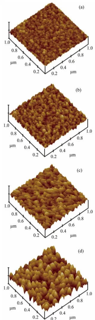
films deposited at different Ti sputtering currents. The average root-mean-square (RMS) roughness of TiZrN films was determined from AFM images in a selected area of 1 μm × 1 μm and the results are shown in Table 1.
It is observed that the RMS roughness increases from 2.73 to 11.58 nm as the Ti sputtering current is increased from 0.6 to 1.2 A.
3.3. Cross-Sectional Morphology
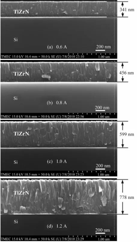
Figure 4 shows the FE-SEM cross-sectional images of
the TiZrN films. All the deposited films show columnar structure which corresponds to the Zone 2 in the Thorn- ton’s structure zone model. It is observed that as the Ti sputtering current increases, the columnar width in- creases and results in the increase of the lateral grain size. The film thickness can be determined from the images in
Figure 4 and the results are shown in Table 1. It is seen
that the thickness of the films increases from 341 to 778 nm when Ti sputtering current is increased from 0.6 to 1.2 A. This result is consistent with the XRD result, that is the intensity of XRD peaks increases with increasing Ti sputtering current.
3.4. TEM Results
Figure 5 shows the TEM selected-area electron diffrac-
Figure 3. AFM images showing surface morphology of the TiZrN films deposited at Ti sputtering currents of : (a) 0.6; (b) 0.8; (c) 1.0 and (d) 1.2 A.
[image:3.595.57.287.323.412.2]Figure 4. Cross-sectional FE-SEM morphology of the TiZrN films deposited at different Ti sputtering currents of: (a) 0.6; (b) 0.8; (c) 1.0 and 1.2 A.
(220) and (311) planes correspond to of fcc B1 type structure of TiN and ZrN in the JCPDS file numbers 87-0633 and 78-1420, respectively, were indexed. It is seen that the spot is brighter as the Ti sputtering in- creases. This indicates the increase in crystallinity of the films. Therefore, the SAED result is in agreement with the XRD result.
3.5. Chemical Composition
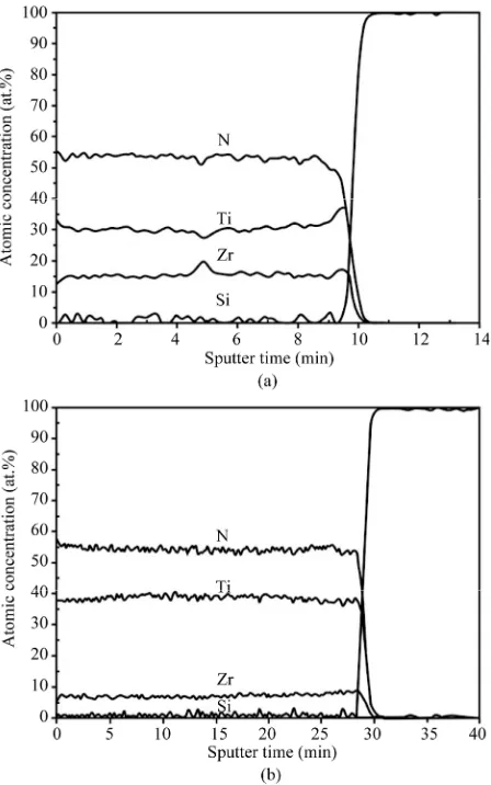
Figure 6 shows the typical AES concentration depth
[image:4.595.351.495.103.628.2]profiles of the TiZrN films deposited at Ti sputtering currents of 0.6 and 1.2 A. A uniform composition dis- tribution of Ti, Zr and N along the depth direction can be seen. The increase of Ti content and the decrease of Zr content can be clearly observed as the Ti sputtering
Figure 5. SAED images of the TiZrN films deposited at different Ti sputtering currents of: (a) 0.6; (b) 0.8; (c) 1.0 and (d) 1.2 A.
current is increased from 0.6 to 1.2 A. The average ato- mic concentration of elements for the TiZrN films was then obtained from the depth profile and the results are given in Table 2.
Figure 6. Depth profiles of the TiZrN films deposited at Ti sputtering currents of : (a) 0.6 and (b) 1.2 A.
Table 2. Chemical composition, Ti content (x value) and N content (y value) in TiZrN films as a function of the Ti sputtering current (ITi).
ITi (A) Ti Zr N x Ti
Ti Zr
= +
N y
Ti Zr
= +
0.6 29.33 19.61 51.06 0.60 1.04
0.8 30.65 17.20 52.15 0.64 1.08
1.0 31.99 14.87 53.14 0.68 1.13
1.2 33.21 12.40 54.39 0.72 1.19
also given in Table 2. It is seen that Ti content increases
from 0.60 to 0.72 when Ti sputtering current is increased from 0.6 to 1.2 A whereas the N content slightly in- creases from 1.04 to 1.19. The N content is more than 1 indicates that all the films prepared in this work are over-stoichiometry.
4. Conclusion
TiZrN films were successfully deposited on Si(100) wa-
fers and carbon coated copper TEM grids by reactive dc magnetron co-sputtering. The Zr sputtering current was fixed at 0.6 A and Ti sputtering current varied from 0.6 to 1.2 A. The effects of Ti sputtering current on the structure and morphology of the films were investigated by XRD, AFM, FE-SEM, TEM and AES. The XRD re- sults revealed that all the prepared films formed (Ti,Zr)N solid solution. The lattice parameter was found to de- crease while the crystallite size, RMS roughness and film thickness increased with increasing Ti sputtering current. This study led to more understanding of the structure, morphology and chemical composition of the films as a function of Ti sputtering current.
5. Acknowledgements
This work was supported by Thailand Centre of Ex- cellent in Physics (ThEP), King Mongkut’s University of Technology Thonburi under The National Research University Project and Vacuum Technology and Thin Films Research Laboratory, Burapha University.
REFERENCES
[1] K. Chu, P. W. Shum and Y. G. Chen, “Substrate Bias Effects on Mechanical and Tribological Properties of Substitutional Solid Solution (Ti,Al)N Films Prepared by Reactive Magnetron Sputtering,” Materials Science and Engineering B, Vol. 131, 2006, pp. 62-71.
http://dx.doi.org/10.1016/j.mseb.2006.03.036
[2] R. Wuhrer and W. Y. Yeung, “Grain Refinement with Increasing Magnetron Discharge Power in Sputter Depo- sition of Nanostructured Titanium Nitride Coatings,” Scripta Materialia, Vol. 50, 2004, pp. 813-818.
http://dx.doi.org/10.1016/j.scriptamat.2003.12.022 [3] K. H. Lee, C. H. Park, Y. S. Yoon and J. J. Lee, “Struc-
ture and Properties of (Ti1-xCrx)N Coatings Produced by
the Ion-Plating Method,” Thin Solid Films, Vol. 385, 2001, pp. 167-173.
http://dx.doi.org/10.1016/S0040-6090(00)01911-8 [4] G. S. Kim, B. S. Kim, S. Y. Lee and J. H. Hahn, “Struc-
ture and Mechanical Properties of Cr-Zr-N Films Synthe- sized by Closed Field Unbalanced Magnetron Sputtering with Vertical Magnetron Sources,” Surface & Coatings Technology, Vol. 200, 2005, pp. 1669-1675.
http://dx.doi.org/10.1016/j.surfcoat.2005.08.101
[5] S. M. Aouadi, T. Maeruf, R. D. Twesten, D. M. Mihut and S. L. Rohde, “Physical and Mechanical Properties of Zirconium Nitride Thin Films,” Surface & Coatings Tech- nology, Vol. 200, 2006, pp. 3411-3417.
http://dx.doi.org/10.1016/j.surfcoat.2005.02.169
[6] H. Hasegawa, A. Kimura and T. Suzuki, “Microhardness and Structural Analysis of (TI,AI)N, (Ti,Cr)N, (Ti,Zr)N, and (TI,V)N, Films,” Journal of Vacuum Science & Tech- nology A, Vol. 18, 2000, pp. 1038-1040.
http://dx.doi.org/10.1116/1.582296
lanced Magnetron Sputtering,” Surface & Coatings Tech- nology, Vol. 185, 2004, pp. 245-253.
http://dx.doi.org/10.1016/j.surfcoat.2003.12.011
[8] O. Knotek, W. D. Munz and T. Keyendecker, “Industrial Aeposition of Binary, Ternary, and Quarternary Nitrides of Titanium, Zirconium and Aluminum,” Journal of Va- cuum Science & Technology A, Vol. 5, 1987, pp. 2173- 2179. http://dx.doi.org/10.1116/1.574948
[9] N. Ichimiya, Y. Onishi and Y. Tanaka, “Properties and Cutting Performance of (Ti,V)N Coatings Prepared by Cathodic Arc Ion Patting,” Surface & Coatings Technol- ogy, Vol. 200, 2005, pp. 1377-1382.
http://dx.doi.org/10.1016/j.surfcoat.2005.08.026
[10] T. Deeleard, S. Chaiyakun, A. Pokaipisit and P. Limsu- wan, “Effects of Vanadium Content on Structure and Chemical State of TiVN Films and Prepared by Reactive DC Magnetron Co-Sputtering,” Materials Sciences and Application, Vol. 4, 2013, pp. 556-563.
http://dx.doi.org/10.4236/msa.2013.49068
[11] J. V. Ramana, S. Kumar, C. David and V. S. Raju “Struc- ture, Composition and Microhardness of (Ti,Zr)N and (Ti,Al)N Coatings Prepared by DC Magnetron Sputter-
[12] V. V. Uglov, V. M. Anishchik, S. V. Zlotski and G. Aba- dias, “The Phase Composition and Stress Development in Ternary Ti-Zr-N Coatings Grown by Vacuum Arc with Combining of Plasma Flows,” Surface & Coatings Tech- nology, Vol. 200, 2006, pp. 6389-6394.
http://dx.doi.org/10.1016/j.surfcoat.2005.11.063
[13] E. W. Niu, L. Li, G. H. Lv, H. Chen, X. Z. Li, X. Z. Yang and S. Z. Yang, “Characterization of Ti-Zr-N Films De- posited by Cathodic Vacuum Arc with Different Substrate Bias,” Applied Surface Science, Vol. 254, 2008, pp. 3909- 3914. http://dx.doi.org/10.1016/j.apsusc.2007.12.022 [14] L. A. Donohue, J. Cawley and J. S. Brooks, “Deposition
and Characterisation of Arc-Bond Sputter TixZryN Coat-
ings from Pure Metallic and Segmented Targets,” Surface & Coatings Technology, Vol. 72, 1995, pp. 128-138. http://dx.doi.org/10.1016/0257-8972(94)02342-5
[15] D. Y. Wang, C. L. Chang, C. H. Hsu and H. N. Lin, “Syn- thesis of (Ti,Zr)N Hard Coatings by Unbalanced Magne- tron Sputtering,” Surface & Coatings Technology, Vol. 130, 2000, pp. 64-68.