Efficient Node Processor with Cycle State Capture Unit
(CSCU) for Secure Intercommunication Module
Kuldeep Chouhan
Research ScholarDr.MGR Educational and Research Institute University,
Chennai - 600095
S.Ravi,Ph.D
Professor and HeadDr.MGR Educational and Research Institute University,
Chennai – 600095
ABSTRACT
An integrated node processor cycle based capture system assures secured serving requests for data. This work introduces a significant extension to the use of operation cycles for network protection. The main function of the operation cycle is to protect path segments and facilitate contiguous working flow. In this paper, the individual nodes have a unique cycle code pattern generated by respective node processor that is kept dynamic for both the node and host/server. A „search cycle code pattern‟ algorithm for fast iterative operation cycle analysis is also proposed.
Keywords
Cycle State Capture Unit (CSCU), Node Processor, Operation Cycle, Network Security.
1. INTRODUCTION
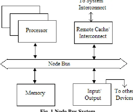
[image:1.595.56.274.568.752.2]In a large network, clients and servers are interconnected and each can be considered as a node processor that offer services to other node processors connected to a specific node [4,7]. A very high proportion of the nodes that offer services need to carry out an authentication process on any node that makes an access request to the node offering the service. Each node contains at least one processor connected in multinode processor system. A local memory for the processor and a remote cache for caching the data obtained from memory on other node processors are used [12]. A node bus system communicates with processor, memory, input/output and interconnect system and all node processors are able to transmit node data to the network node processor, as shown in Figure 1.
Fig. 1 Node Bus System
1.1 Efficient Node Processor
An efficient design for intercommunication, can communicate among processes within a node or on different nodes. A node processor operates based on the usual metrics of latency and throughput also includes [5,10],
(i) Scalability
(ii) Effects of data transfer operation on node processor
(iii) Application data located in the processor
1.2
Node Processor Locate Code Buffer
Pattern
A node processor technique allocates a segmented code buffer located in a region. This mechanism sends processor code data from the source buffer into the shared buffer CSCU (receiver) located in the destination buffer. The synchronization is required to make sure that processor code data need not read the buffer before the other code instruction has finished writing and vice versa.
1.3
CSCU
Hardware Description
The hardware description work as CSCU that checks whether the instruction captured unit is matched with given inputs. This mechanism is possible through a trigger input button pressed one by one and receives each byte instruction (signal) shows that where is signal stand on that flash. This is required fed as input for cycles, which is connected with CSCU. This hardware board has pin configuration also to display the captured cycle unit to get corrected cycle operations. The CSCU has hold, opcode fetch (F), memory read (MR), memory write (MW), input/output read and write as shown in Figure 2.
[image:1.595.317.544.579.753.2]2.
NODE
PROCESSOR
AUTHENTICATION METHODOLOGY
In this section, node processor methodology authenticate a processor with an operation cycle that captured instructions to follow via CSCU and check the status of captured code unit and make sure that the transmission possibility of instructions in the node processor are accurate.
2.1
Applying Cycle Consistency Matrix
to Absorbing Sets
The cycle consistency matrix captures the cycle behavior, while the cycle consistency matrix approach [1,6,8,9,10,11,13] is applicable to graphical structures that contain CSCU.
2.2
Public Key Using by Trusted Nodes
The public keys embedded in certificates are used to verify that the received content has been created and signed by trusted nodes [7,12,17]. Trusted content is accepted while untrusted content is rejected [2,3,4,23]. To reduce the overhead of rejections, only the metadata header of the content processor data has to be received for a reject/accept in an operation cycle [18,19].3. INFORMATION OPERATION CYCLE
PROCESS
The cyclic operations occur in a wide range of fields with its computations and feedback control. The characteristics of these operations are that the same operations are repeated continuously. If an internal input state vector is changing, resulting in different outputs, the operations cycle does not match with CSCU (receiver) output. Consequently, multiple operation elements are used when processor elements are unable to provide the necessary computational operations to meet trusted elements. Information processing cycle of system consists of,
(i) Input: Enter processor data into the system.
(ii) Processing: Perform operations cycle on the processor data.
(iii) Output: Present the results.
3.1
Node Processor Timing Bus Operation
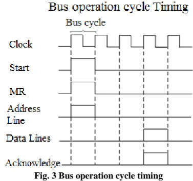
[image:2.595.332.521.73.250.2]Each processor bus cycle consists of at least four clock (CLK) cycles. The address is emitted from the processor during processor time and node data transfer occurs on the bus operation. It is used primarily for changing the direction of the bus during memory read (MR) operations, which is shown in Figure 3.
Fig. 3 Bus operation cycle timing
3.2
Design Phase of Operation Cycle
The design phase approach of operation cycle process are needed to complete an code instruction as well as the precedence relationships to determine the operation cycle time duration of the cycle design phase [21,22,24,25]. It is a complex stage and longest phase by a significant amount of a cycle completion. The operation cycle state model used several processes to estimate the cycle time with a more composite process model of the design phase.
3.3 Preselection Approach for CSCU
A large number of node processor involves a huge number of operation cycles states and can lead to the problem of unsolvable in a bounded time cycle process [14,15,16,20]. For a CSCU design with finite operation cycles, the cycles are periodic. A cycle with a larger credit, which locates at some prior position in the sequence, therefore, has more chances to be selected for the completion of an operation cycle. To evaluate the performance of this approach, the hardware unit accomplishes the random cycle selection CSCU. An operation cycle pattern approach achieves a better performance than the random selection approach. This new definition is a more effective one for the operation cycle design for a capture unit, which is given in eqn. [1],
… (1)
where, D is set of demand cycle pairs on the traffic cycle matrix, indexed by r. Sr is set of operation traverse by the path between demand cycle pair. Here, we assume there is only a single shortest path existing between each demand cycle pair. P(j) denotes cycle set P.k enumerates on cycle P(j) and represents the captured unit k. In this paper, we used the distance point between the cycle nodes that connected to represent the cycle, ck. γri,j and gr denotes number of traffic cycle units of the flow between demand cycle pair r. Lr is the length of the flow of demand cycle pair r.
next operation until all operations agree on a set of cycle outputs. Therefore, the expected number of iterations for cycle operation is for k = 1,2,…,n, is given in eqn. [2],
1
1 2 1
0 1 ( )
1 1
...
1 .( 1 ) . ( ). .(1 k )
K
n
i k m j
A m p p j
i j
N i n j
1 2 1 0 12 ( )
1
1
( ).
.(1
)
...
(1
1
)
kn
k m j
m p p j
j
j
n
… (2)where, Π0
p=1 Гp = 1 and Π-1m=0 Гσm (j) = 1 for j. Here, Гk specify ГAk and σ is a function: {1,2,…,n} →{1,2,…,n} such that σ (i) = i+1, i=1,2,…,n-1, and σ(n) = 1. In additional , σk
(i) is a kth cycle relation such that σk(i) = i+k. When these operations are repeated, it estimated the cycle‟s estimation, as given in [3],
… (3) where, N*Ak = NAk + 1 and TA0,A1 = TAn,A1. Another term is used to compensate for the overestimated elapsed of operation cycle.
When the cycle communication process is moved forward only if two or more operations simultaneously on a set of cycle design. It exists communication cycle pattern among all operations A1, A2, …, An, if IAi = U
n
j=1OAj,each operation is simultaneously repeated until all other operations captured units. Therefore, the expected number of iterations in a communicate cycle pattern is given in eqn. [4],
1
1 1
1
1
(1
(1
))
.
(1
)
1
.
(1
)
i i
i
n k n
A A i i k n A i
N
k
… (4)With probability (1 - Πni=1 (1-ГAi)), the cycle pattern fails to distribute the captured unit in a given iteration and repeat the operation cycle. Then, the operation cycle pattern compute by adding of each operation until the cycle pattern is completed, is given in eqn. [5],
*
max max
1
. ( ) ( ). . ( ) .
1,..., i 1,..., i
N
Ai A Ai A
k
D l x N N D l N N
i n i n
… (5)where, N* =N+1 and σ is the average communication cycle pattern per iteration for CSCU.
3.4
Algorithm: Search Cycle Code Pattern
Step 1: Start processStep 2: Compute for a complete cycle with F, MR, MW, IOR, IOW, and INA (cycle can start anywhere in iteration). Step 3: Search a cycle code pattern.
Step 4: Check whether the process operation is same or different.
Step 5: if same follow Step 2
Step 6: else Step 7: End process
4.
IMPLEMENTATION
ON
[image:3.595.316.545.173.345.2]HARDWARE DESCRIPTION PROCESS
The hardware description of the CSCU and interprocess communication module is shown in Figure 4. All the processor nodes transmit node data to CSCU.Fig. 4 CSCU and Interprocess Communication Module
4.1 Multiplexed Bus Cycle Timing
[image:3.595.316.546.467.552.2]The multiplexed bus cycle timing execution program consists of a sequence of MR and MW operations each of which transfers a bytes of data between memory and I/O. These operations (communicated between the processor and the other elements) are necessary to execute any instruction. Every time state has clock pulse with each memory instruction either MR or MW, as shown in Figure 5.
Fig. 5 CSCU timing for Store Accumulator Direct (SAD) instruction
4.2 State Transition Sequence
Table 1. Node processor data consist operation cycles Operation
Cycle
Status Control IO
/M S 1
S 0
R D
W R
IN TA
Opcode Fetch (F)
0 1 1 0 1 1
Memory Read (MR)
0 1 0 0 1 1
Memory Write (MW)
0 0 1 1 0 1
I/O Read (IOR)
1 1 0 0 1 1
I/O Write (IOW)
1 0 1 1 0 1
INTA Acknowledg
e (INA)
1 1 1 1 1 0
Bus Idle (BI) DAD 0 1 0 1 1 1 INA
RST/ TRAP
1 1 1 1 1 1
HALT 15 0 0 15 15 1
The actual number of states required to perform any instruction depends on the instruction being executed, the particular operation cycle within the instruction cycle.
5.
TYPICAL
NODE
PROCESSOR
OPERATIONS CYCLE
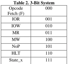
[image:4.595.313.546.191.422.2]Every operation cycle can be identified by decoding the status lines S0, S1 and IO/M'. The 3-bit identified one complete cycle for a node is given in Table 2.
Table 2. 3-Bit System
Opcode Fetch (F)
000
IOR 001
IOW 010
MR 011
MW 100
NoP 101
HLT 110
State_x 111
[image:4.595.99.235.456.582.2]An example operation cycle is shown in Table 3 and Table 4.
Table 3. Address Instruction for Node_1 Node_1 Cycles
8000 MVI A, 46 2T
8002 STA 3200 3T (Internally 4T)
8005 JMP 8000
Table 4. Address bit system for a complete cycle state Node_2 Cycles
8000 MVI A, 36 F +MR
8002 MOV B, A F
8003 ADD A F
8004 MVI A, 46 F + MR
8006 JMP 8000 F + MR + MR
Totally 27 bits are used to transmit one complete cycle as shown in Figure 6 and Figure 7.
For Node_1:
F + MR + F + MR + MR + MW + F + MR + MR
Fig. 6 One cycle of bits for node_1 processor For Node_2:
F + MR + F + F + F + MR + F + MR + MW
Fig. 7 One cycle of bits for node_2 processor
[image:4.595.321.543.465.594.2]Figure 8 shows the possible iteration which make sure that the server side authenticating unit can operate from any cycle to decode the correct cycle.
Fig. 8 Iteration Process for Node_1
6. RESULTS AND DISCUSSION
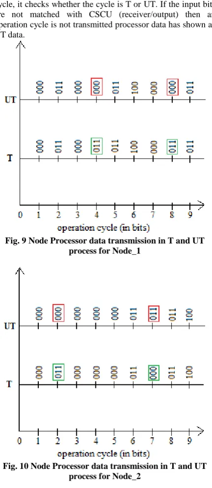
The node processor data is transmitted for a cycle in Trusted (T) or Untrusted (UT) form for Node_1 and Node_2, which is shown in Table 5.
Table 5. Trusted (T) and Untrusted (UT) Node Processor Data for Node_1 and Node_2
Data (in bits)
Node_1 Node_2 T UT T UT
1 000 000 000 000
2 011 011 011 000
3 000 000 000 000
4 011 000 000 000
5 011 011 000 000
[image:4.595.63.272.614.761.2]7 000 000 000 011
8 011 000 011 011
9 011 011 100 100
[image:5.595.63.269.73.113.2]In Figure 9 and Figure 10 shows when node data transmission occurs for Node_1 and Node_2 to complete an operation cycle, it checks whether the cycle is T or UT. If the input bits are not matched with CSCU (receiver/output) then an operation cycle is not transmitted processor data has shown as UT data.
Fig. 9 Node Processor data transmission in T and UT process for Node_1
Fig. 10 Node Processor data transmission in T and UT process for Node_2
7. CONCLUSION
In this work, CSCU system works as receiver and integrated captured units to check a correct cycle operation code pattern. It concluded that if we segment the instructions code then CSCU for each processor verify byte data unit for all node processor to provide a correct and trusted response to host and cooperated to assure a reliable node processor unit to transmit data in network security scheme.
8. ACKNOWLEDGEMENT
The authors heartly thank to M/s. MicroLogic Systems, Chennai-600017, for the infrastructure to carry out this work successfully.
9. REFERENCES
[1] A. Shokrollahi and R. Storn, “Design of efficient erasure codes with differential evolution”, in proceeding International Symposium Information Theory, Sorrento, Italy, June 2000.
[2] Alexander Shraer, Christian Cachin, Asaf Cidon, Idit Keidar, Yan Michalevsky, “Venus: Verification for Untrusted Cloud Storage”, CCSW‟10, Chicago, Illinois, USA, October 8, 2010.
[3] Billy K. H. Wong, and Henry Shu-hung Chung, “Steady-State Analysis of PWM DC/DC Switching Regulators Using Iterative Cycle Time-Domain Simulation”, IEEE Transactions on Industrial Electronics, Vol. 45, No. 3, June 1998.
[4] Chong-Fatt Law, Bah-Hwee Gwee and Joseph S. Chang, “Asynchronous Control Network Optimization Using Fast Minimum-Cycle-Time Analysis”, IEEE Transactions On Computer-Aided Design Of Integrated Circuits And Systems, Vol. 27, No. 6, June 2008. [5] C. Cachin, I. Keidar and A. Shraer, “Fail-aware untrusted
storage”, in proceeding International Conference on Dependable Systems and Networks (DSN-DCCS), pages 494–503, 2009.
[6] C. Cachin, A. Shelat, and A. Shraer, “Efficient fork-linearizable access to untrusted shared memory”, in proceeding 26th ACM Symposium on Principles of Distributed Computing (PODC), pages 129–138, 2007. [7] D. L. Rosenband, “Synthesis of multi-cycle
operation-centric descriptions”, Ph.D. Dissertation Proposal, Massachusetts Institute of Technology, June 2000. [8] D. J. C. MacKay, “Good error correcting codes based on
very sparse matrices”, IEEE Transactions Information Theory, vol. 45, pp. 399–431, Mar. 1999.
[9] E.-J. Goh, H. Shacham, N. Modadugu and D. Boneh, “SiRiUS: Securing remote untrusted storage”, in proceeding Network and Distributed Systems Security Symposium (NDSS), 2003.
[10]Gangxiang Shen and Wayne D. Grover, “Extending the p-Cycle Concept to Path Segment Protection for Span and Node Failure Recovery”, IEEE Journal on Selected Areas in Communications, Vol. 21, No. 8, October 2003. [11]Gregory Lucas, Chen Dong, and Deming Chen,
“Variation-Aware Placement with Multi-Cycle Statistical Timing Analysis for FPGAs”, IEEE Transactions On Computer-Aided Design Of Integrated Circuits And Systems, Vol. 29, No. 11, November 2010.
[12]Hong-Bae Jun, Hyun-Soo Ahn, and Hyo-Won Suh, “On Identifying and Estimating the Cycle Time of Product Development Process”, IEEE Transactions On Engineering Management, Vol. 52, No. 3, August 2005. [13]Jiadong Wang, Lara Dolecek and Richard Wesel, “The
Cycle Consistency Matrix Approach to Absorbing Sets in Separable Circulant-Based LDPC Codes”, IEEE 6th International Symposium on Turbo Codes and Iterative Information Processing in Brest, France, Dec 2012. [14]J. Wang, L. Dolecek and R.D. Wesel, “Controlling
LDPC absorbing sets via the null space of the cycle consistency matrix”, in proceeding IEEE International Conference on Communication (ICC), Kyoto, Japan, Jun. 2011.
[image:5.595.60.276.145.641.2]Transactions Communication 52(7):1038–1042, Jul. 2004.
[16]L. Decreusefond and G. Zémor, “On the error-correcting capabilities of cycle codes of graphs”, Comb., Probab., Computing, no. 6, pp. 27–38, 1997.
[17]M. Kallahalla, E. Riedel, R. Swaminathan, Q. Wang, and K. Fu., Plutus: Scalable secure file sharing on untrusted storage”, in proceeding 2nd
USENIX Conference on File and Storage Technologies (FAST), 2003.
[18]Rebecca Copeland, “Policies to Enable Serving Untrusted Services on Alternative (non-3GPP) and Untrusted Access Networks in EPS”, 3rd International IEEE Workshop on Open NGN and IMS Testbeds: Next Generation Network Evolution Towards the Future Internet, Munich: Germany, 2011.
[19]R. Sekar, A. Gupta, J. Frullo, T. Shanbhag, A. Tiwari, H. Yang and S. Zhou, “Specification-based anomaly detecion: A new approach for detecting network intrusions”, in ACM Computer and Communication Security Conference (CCS‟02), Washington, DC, USA, Nov. 18-22 2002.
[20]R. Asvadi, A. H. Banihashemi, and M. Ahmadian-Attari, “Lowering the error floor of LDPC codes using cyclic liftings”, IEEE Transactions Information Theory, 57(4):2213–2224, Apr. 2011.
[21]R. Asvadi, A. H. Banihashemi and M. Ahmadian-Attari, “Design of finite-length irregular protograph codes with low error floors over the binary-input AWGN channel using cyclic liftings”, IEEE Transaction Communication, 60(4):902–907, April 2012.
[22]T. Tian, J. D. Villasenor and R. D. Wesel, “Selective avoidance of cycles in irregular LDPC code construction”, IEEE Transaction Communication, 52(8):1242–1247, Aug. 2004.
[23]U. Maheshwari, R. Vingralek and W. Shapiro, “How to build a trusted database system on untrusted storage”, in proceeding 4th Symposium Operating Systems Design and Implementation (OSDI), pages 135–150, 2000. [24]W. L. Pearn, Yu-Ting Tai and J. H. Lee, “Statistical
Approach for Cycle Time Estimation in Semiconductor Packaging Factories”, IEEE Transactions On Electronics Packaging Manufacturing, Vol. 32, No. 3, July 2009. [25]Yan Qiao, NaiQi Wu and MengChu Zhou, “A Petri
Net-Based Novel Scheduling Approach and Its Cycle Time Analysis for Dual-Arm Cluster Tools With Wafer Revisiting”, IEEE Transactions On Semiconductor Manufacturing, Vol. 26, No. 1, February 2013.
BIOGRAPHIES
Kuldeep Chouhan was born on November 12th 1984 and got his M.Tech. (CSE) degree, in the year 2009. He is a Research Scholar in Dr. MGR Educational and Research Institute University, Chennai. He published Three International journals and one International conference. His area of interests is Wireless Sensor Network (WSN), Image noisy filter, Embedded system and Intelligent System.