WRL
Research Report 91/4
TurboChannel
T1 Adapter
research relevant to the design and application of high performance scientific computers. We test our ideas by designing, building, and using real systems. The systems we build are research prototypes; they are not intended to become products.
There is a second research laboratory located in Palo Alto, the Systems Research Cen-ter (SRC). Other Digital research groups are located in Paris (PRL) and in Cambridge, Massachusetts (CRL).
Our research is directed towards mainstream high-performance computer systems. Our prototypes are intended to foreshadow the future computing environments used by many Digital customers. The long-term goal of WRL is to aid and accelerate the development of high-performance uni- and multi-processors. The research projects within WRL will address various aspects of high-performance computing.
We believe that significant advances in computer systems do not come from any single technological advance. Technologies, both hardware and software, do not all advance at the same pace. System design is the art of composing systems which use each level of technology in an appropriate balance. A major advance in overall system performance will require reexamination of all aspects of the system.
We do work in the design, fabrication and packaging of hardware; language processing and scaling issues in system software design; and the exploration of new applications areas that are opening up with the advent of higher performance systems. Researchers at WRL cooperate closely and move freely among the various levels of system design. This allows us to explore a wide range of tradeoffs to meet system goals.
We publish the results of our work in a variety of journals, conferences, research reports, and technical notes. This document is a research report. Research reports are normally accounts of completed research and may include material from earlier technical notes. We use technical notes for rapid distribution of technical material; usually this represents research in progress.
Research reports and technical notes may be ordered from us. You may mail your order to:
Technical Report Distribution
DEC Western Research Laboratory, WRL-2 250 University Avenue
Palo Alto, California 94301 USA
Reports and notes may also be ordered by electronic mail. Use one of the following addresses:
Digital E-net: DECWRL::WRL-TECHREPORTS
Internet: [email protected]
UUCP: decwrl!wrl-techreports
David Boggs
Abstract
This report is the technical reference for the T1D4PKT adapter, a
communica-tion opcommunica-tion module for TurboChannel I/O systems. It uses basic HDLC (flags,
bit-stuffing, CRC) to send and receive packets over a T1 circuit with D4 framing
(1.544 Mb/s digital telephone circuit). The adapter was designed for use in packet
switching routers linking local area networks into metropolitan-area and wide-area
networks.
This adapter is a research prototype; it is not a product.
Copyright
1991 Digital Equipment Corporation
1. Overview
The T1D4PKT adapter is a communication option module for TurboChannel I/O systems. It uses basic HDLC (flags, bit-stuffing, CRC) to send and receive packets over a T1 circuit with D4 framing (1.544 Mb/s digital telephone circuit). The adapter was designed for use in packet switching routers linking local area networks into metropolitan-area and wide-area networks.
The adapter’s electrical interface is DSX-1 and its physical interface is an RJ48 modular telephone jack. The Data Service Unit (DSU) function is included in the adapter, so it can directly connect to a Channel Service Unit (CSU), a multiplexer, etc.
Figure 1 shows some possible configurations for connecting two packet routers with a T1 cir-cuit. The top connection shows a T1 circuit using wire pairs provided by a telephone company; the two central offices could be in the same city or on opposite coasts. The middle connection shows a T1 circuit multiplexed with three other T1 circuits, perhaps containing voice channels, and carried over a microwave radio T2 link; maximum distance is about 15 kilometers between radios. The bottom connection shows a T1 circuit multiplexed with twenty-seven other T1 cir-cuits and carried over a private fiber optic T3 link. Digital Equipment Corporation owns and operates a fiber optic network connecting most company sites in New England.
CO
M13 = T1/T3 Muitiplexer RAD = Microwave Radio CSU = Channel Service Unit M12 = T1/T2 Multiplexer
FR FR M13
RAD M12 CSU NI NI RAD M12 CSU T1 D4 PKT T1 D4 PKT T1 D4 PKT T1 D4 PKT T1 D4 PKT E T H E R N E T E T H E R N E T Router Router D S 5 0 0 0 C P U T1 D4 PKT
FR = Fiber Repeater LR = Line Repeater NI = Network Interface CO = Central Office D S 5 0 0 0 C P U M13 FR
[image:4.612.96.555.335.534.2]LR CO LR
Figure 1: Some Possible Configurations
2. Installation Information
Two LEDs are visible through a hole next to the modular connector. The Carrier LED lights when the adapter is seeing a legal T1 signal. The FrameSync LED lights when the adapter has synchronized with the D4 framing pattern imbedded in the T1 bit stream. The LEDs correspond to bits by the same name in the control/status register. Both LEDS must be lit for the adapter to work. Carrier c c c c c c c c c d c c c c c c c c c c c c c c r r RxFSM1 CtlReg1 Connector TxCRC TxCRC 240 377 377 863 RxCRC RxCRC RxFSM2 RxFSM0 OptionRom CtlReg0 CtlReg2 TxFifo RxFrame
[image:5.612.124.463.138.567.2]Rx2Cntr RxFifo Tx2Cntr TxFrmCntr RxFrmRom RxFrmCntr RxDataSR TxDataSR TxFrame TxFSM2 TxFSM0 TxFSM1 RJ48 374 liu Osc d Xfmr LIU Xtl C C C C FrameSync
Figure 2: Option Module Layout
The application driving the design of this adapter was a router that forwards packets between Ethernet local networks. The maximum size of an Ethernet packet is 1518 bytes; The maximum packet size of this adapter is 2048 bytes. The limiting factor is the size of FIFO ICs, currently 4K bytes. Since the capacity of a FIFO chip can grow without changing its pinout, maximum packet size can be increased as bigger FIFOs become available simply by loading different ICs.
Two types of connectors are used on T1 equipment: an 8-pin modular telephone connector designated RJ48 by the FCC, and a 15-pin D-series subminiature connector. This adapter uses the new RJ48 connector, but it may connect to equipment using the older DA15 connector. Figure 3 shows the corresponding pins in the two connectors. If the other equipment has a modular jack, then the cable is wired straight through. A null modem cable connecting two nearby adapters with wire and no electronics, turns over the transmit and receive pairs between the two connectors. Looking into the cable entry hole on a modular plug with the locking tab oriented up, pin one is on the right; DA15 connectors have pin numbers molded into the plastic shell.
10 11 RJ48 DA15
8 1 2 7 4 5
3 2 9 1 Signal
Xmt Ring Xmt Tip
Rcv Ring 1 Rcv Tip 1 ground
ground shield ground
Net to Adapter Net to Adapter shield ground Adapter to Net Adapter to Net
[image:6.612.206.452.293.448.2]Direction
Figure 3: Connector Pins
3. What is T1?
T1 was developed at Bell Laboratories in the late 1950s, and the first commercial system was installed in 1962 [20] [21] [22] [23]. Urban cable conduits and manholes were filling up and it was becoming necessary to carry more than one voice channel on a wire pair. Silicon transistors were available, making possible low-power high-reliablility line repeaters. Digital technology was maturing; all previous multiplexing schemes used analog technology. 24 analog voice chan-nels were converted to 8-bit digital samples 8000 times per second, for a combined data rate of 1.536 Mb/s. Between each frame of 24 samples (192 bits), an overhead bit was inserted for synchronizing terminal equipment at the ends of a circuit, making the total bit rate 1.544 Mb/s. Bell System multiplexing schemes traditionally were assigned letter designations, and this first digital system was named T-carrier; the electrical format was named DS1, for Digital Signalling level 1. A 64 Kb/s voice or data channel is level 0 of the hierarchy; multiplexers combine several bit streams from a lower level in the hierarchy to form a higher level bit stream. Figure 4 summarizes the hierarchy of digital transmission systems that has evolved over the last three decades [2] [10] [15].
DS4 DS3 DS2 DS1 DS0 Level
Voice Channel Components
0.064 Mb/s
1.544 Mb/s
274.176 Mb/s 44.736 Mb/s 6.312 Mb/s Bit Rate
24 DS0s
4 DS1s
7 DS2s
[image:7.612.175.408.293.429.2]6 DS3s
Figure 4: Digital Hierarchy
A T1 signal is a sequence of pulses 3 volts high and 324 nanoseconds wide. The presense of a pulse in a bit cell represents one data value and the absense of a pulse represents the other binary value. Pulses alternate in polarity, making it a 3-level code: +3v, 0 and -3v. This Alternate Mark Inversion, or AMI code, has no DC signal component and the highest fundamental fre-quency component is half the bit rate. A bit error, changing a pulse into a no-pulse or vise-versa, results in two pulses of the same polarity, called a bipolar violation. Figure 5 shows a T1 signal with a bipolar violation near the end of the bit string.
+3V
0V
-3V
1 1 1 1 0 0 0 1 1 0 1 1 V 1 1
324 ns
[image:7.612.66.518.600.680.2]Timing information, defining when a receiver should sample the value of a bit, is recovered from the pulse stream, so a T1 signal must contain a minimum pulse density. The average pulse density must be at least 12.5%, or one pulse in eight bit cells, and there must be no more than 15 consecutive bit cells in which no pulse is present. Channel Service Units are required to insert pulses into a T1 stream if the pulse density is too low. As will be explained below, HDLC bit stuffing guarantees that the bit stream produced by this adapter meets the pulse density require-ment.
When equipment can’t guarantee meeting the pulse density requirements, a scheme called Bipolar with 8 Zero Substitution or B8ZS is used. B8ZS replaces eight consecutive bit cells that contain no-pulses with a sequence of pulses containing a distinctive bipolar violation. Normally, intermediate equipment in a circuit removes bipolar violations, but when a circuit is ordered with the B8ZS feature, these particular bipolar violations are not eliminated and are not counted as errors. This adapter never generates long strings of no-pulses so it does not use B8ZS.
The clock used by a T1 transmitter may come from a local oscillator (local or master timimg), or from the received pulse stream (loop or slave timing) [1] [8]. Local oscillators can be as much as 75 bits per second fast or slow, so multiplexers must be prepared to handle unsynchronized pulse streams. Currently, most point-to-point circuits offered by common carriers go through such asynchronous multiplexers and the end-user equipment must provide timing [5] [9] [11]. As analog transmission equipment is retired from service and digital VLSI continues to spread, carriers are installing a new generation of synchronous multiplexers which require all transmit-ters to be frequency-locked to a single timing source provided by the network and recovered from the received pulse stream [12] [14].
Timing jitter, or short-term variations of the significant instants (when to sample the values of bits) from their ideal positions in time, is a big problem for T1 (and token rings and FDDI for similar reasons). Line repeaters introduce pattern-dependent jitter [25] and multiplexers intro-duce waiting time jitter [24]. Long-term variations, called wander, are caused by such things as daily temperature variation in pole-mounted cable which can change the electrical length of a circuit by many bits. This adapter includes a wander and jitter attenuator which meets all re-quirements for operation while frequency-locked to the received pulse stream [9] [18].
The framing bit pattern is the sequence of overhead bits inserted between groups of 24 8-bit samples. While twisted pairs and line repeaters do not distinguish frame bits from data bits, multiplexers usually require that T1 signals contain a framing pattern. D4, the most common framing format and the one implemented by this adapter, consists of the 12-bit repeating se-quence 100011011100 [6] [17]. A new framing format called Extended Super Frame or ESF, uses some of the frame bits as a checksum over preceding data bits, and other frame bits as a low-speed data link for monitoring and controlling equipment in the circuit. There are two com-peting standards for how to use the facility data link in ESF: AT&T [7] and BellCore [13] do it one way, and ANSI [3] does it a different way; manufacturers offer both versions.
Europe adopted the good ideas from the American digital telephone system, and fixed many of its faults. Consequently European T1, called E1, is similar but not compatible. The bit rate is 2.048 Mb/s, or 32 8-bit samples 8000 times per second. Coax cable is often used rather than twisted wire pairs. High Density Bipolar order 3, or HDB3 coding, replaces four consecutive no-pulses with a 4-bit sequence containing a bipolar violation, similar to B8ZS. Frame bits are not sprinkled in between groups of bytes as in T1, but rather two time slots, bytes 0 and 16, are reserved for synchronization patterns, checksums, and facility data link, similar to ESF. This format is called PCM30, because it carries 30 Pulse Code Modulation voice channels.
There is much more to T1 than has been explained here, but most of it only applies to circuits carrying voice channels. The T1 signal generated by this adapter resembles 24 PCM voice chan-nels just enough to easily pass through telephone networks.
4. What is HDLC?
Synchronous Data Link Control, or SDLC [27] [28], was developed by IBM in the late 1960s as an improvement over BiSync [26], an older method for sending packets over a serial link. During the 1970s various standards bodies adopted modified versions: the American National Standards Institute called their version Advanced Data Communication Control Procedure or ADCCP [4]; The International Standards Organization called their version High-Level Data Link Control or HDLC [19].
The good idea in SDLC is bit stuffing (as opposed to byte stuffing used in BiSync) to distin-guish control information from user data. Between packets, an idle transmitter sends continuous Flags: (01111110). If the eight bits after a flag are not also a flag, then they are the first eight bits of a packet. Within a packet, a transmitter stuffs, or inserts, a 0-bit after five consecutive 1-bits; a receiver unstuffs, or deletes, a 0-bit after five consecutive 1-bits. Bit stuffing prevents data patterns from looking like flags. Six or more consecutive 1-bits terminates a packet. If there are exactly six consecutive 1-bits (another flag) then the packet ends normally. If there are seven or more 1-bits (an Abort) then the packet is damaged and should be discarded.
The bytes just before a packet’s ending flag are a Cyclic Redundancy Checksum or CRC. The CRC is calculated by the transmitter, appended to the end of the data before the flag, and checked by the receiver. If the CRC is not correct, the packet is damaged and should be dis-carded. The CRC is the remainder after dividing the packet bits by a polynomial. When the receiver does the same division on the incoming packet bits including the CRC, the result should be zero.
Bit stuffing can be used to satisfy the pulse density requirements of a T1 circuit by encoding a 0-bit as a pulse and a 1-bit as a no-pulse. This is called Inverted HDLC because voice channels traditionally encode 1-bits as pulses (all ones is more correctly called all pulses). The worst case happens when a pulse frame bit falls in an HDLC flag, resulting in seven consecutive no-pulses, which is 12.5% pulse density.
5. What is a TurboChannel?
A TurboChannel is a synchronous asymmetric input/output bus designed by Digital Equip-ment Corporation for use in workstations [29] [30] [31]. It is synchronous because there is a global clock whose rising edge is the reference for all bus signals. It is asymmetric because there is one system module and some number of option modules connected to it. The system module can read and write the option modules, and option modules can read and write the system module, but option modules can’t talk to each other.
When a program running in the system module executes a load or store instruction whose effective address falls within the address space of an option module, an I/O read or I/O write bus transaction is performed. The system module asserts a signal selecting an option module, and places an address on the 32-bit address/data bus, which the option module saves in a register. In the next cycle the system module reads or writes a word; if the option module is not ready, it can assert a signal to stall the transaction.
For DS5000 systems, I/O reads and writes to the adapter should use addresses in the uncached and unmapped KSEG1 memory region (the base address of I/O slot 0 is 0xBE000000 and that of slot 1 is 0xBE400000). A DS5000/200 can do 5 I/O writes or 2 I/O reads per microsecond. The T1 transmitter requires an I/O write and the receiver requires an I/O read about every 5 microseconds when going full-tilt boogey.
An option module can read and write main memory via the system module by performing a Direct Memory Access or DMA bus transaction. An option module asserts a read or write signal to start a DMA operation, and then waits for an acknowledgement from the system module. Upon receipt of an ack, the option module drives an address onto the bus and then writes, or after a pause, reads 32-bit words on each succeeding cycle, for a peak bandwidth of 100 MBytes/sec (one 32-bit word every 40 ns = 800 Mbits/sec = 100 MBytes/sec). At 192 KBytes/sec each way, this adapter does not use DMA.
The TurboChannel clock can be any fixed frequency between 12.5 and 25 MHz. For slow TurboChannels, the IOCTL2 PAL at position E14 must be changed. The fast PAL works from 27 MHz to 15.6 MHz (DS5000/200); the slow PAL works from 16.6 MHz to 7.8 MHz (DS5000/1xx). This will be fixed somehow in the next artwork revision.
There is nothing more to the TurboChannel; it is refreshingly simple. Many of DEC’s I/O buses are asynchronous and symmetric, making them slow and complex, and raising the cost to implement simple devices.
6. Programming Interface
The T1D4PKT adapter is a programed I/O device; it does not use DMA. A device driver communicates with the adapter by executing load and store instructions whose effective ad-dresses are within the adapter’s 4 MByte address space.
There are three regions in the adapter address space: control/status, data, and option rom. •The Control/Status Register (CSR) is a single address. Some of the bits in this
•The Data Register is a single address to which transmitter bytes are written and from which receiver bytes are read. Even though the transmitter and receiver are completely independent of each other, their data registers share the same I/O ad-dress.
•The Option ROM occupies 128K addresses in the adapter’s space. It contains infor-mation about the adapter (type, manufacturer, revision level, etc) and diagnostic programs that can be loaded into memory and executed under the ROM Executive.
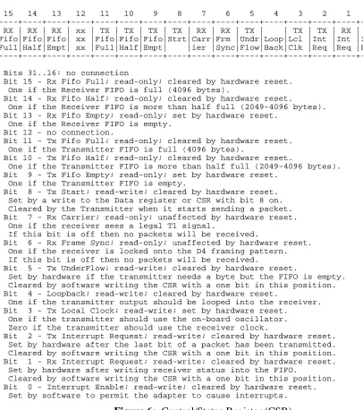
6.1. Control/Status Register
The control/status register, figure 6, is addressed when the adapter is selected and address bits 17 and 4 are one. Other address bits are ignored, so there are many other I/O addresses which will also reference the CSR.
[image:11.612.61.467.255.713.2]15 14 13 12 11 10 9 8 7 6 5 4 3 2 1 0 +----+----+----+----+----+----+----+----+----+----+----+----+----+----+----+----+ | RX | RX | RX | xx | TX | TX | TX | TX | RX | RX | TX | | TX | TX | RX | | |Fifo|Fifo|Fifo| xx |Fifo|Fifo|Fifo|Strt|Carr|Frm |Undr|Loop|Lcl |Int |Int |Int | |Full|Half|Empt| xx |Full|Half|Empt| |ier |Sync|Flow|Back|Clk |Req |Req |Enbl| +----+----+----+----+----+----+----+----+----+----+----+----+----+----+----+----+
Bits 31..16: no connection
Bit 15 - Rx Fifo Full; read-only; cleared by hardware reset. One if the Receiver FIFO is full (4096 bytes).
Bit 14 - Rx Fifo Half; read-only; cleared by hardware reset.
One if the Receiver FIFO is more than half full (2049-4096 bytes). Bit 13 - Rx Fifo Empty; read-only; set by hardware reset.
One if the Receiver FIFO is empty. Bit 12 - no connection.
Bit 11 - Tx Fifo Full; read-only; cleared by hardware reset. One if the Transmitter FIFO is full (4096 bytes).
Bit 10 - Tx Fifo Half; read-only; cleared by hardware reset.
One if the Transmitter FIFO is more than half full (2049-4096 bytes). Bit 9 - Tx Fifo Empty; read-only; set by hardware reset.
One if the Transmitter FIFO is empty.
Bit 8 - Tx Start; read-write; cleared by hardware reset. Set by a write to the Data register or CSR with bit 8 on. Cleared by the Transmitter when it starts sending a packet. Bit 7 - Rx Carrier; read-only; unaffected by hardware reset.
One if the receiver sees a legal T1 signal.
If this bit is off then no packets will be received.
Bit 6 - Rx Frame Sync; read-only; unaffected by hardware reset. One if the receiver is locked onto the D4 framing pattern. If this bit is off then no packets will be received.
Bit 5 - Tx UnderFlow; read-write; cleared by hardware reset.
Set by hardware if the transmitter needs a byte but the FIFO is empty. Cleared by software writing the CSR with a one bit in this position. Bit 4 - Loopback; read-write; cleared by hardware reset.
One if the transmitter output should be looped into the receiver. Bit 3 - Tx Local Clock; read-write; set by hardware reset.
One if the transmitter should use the on-board oscillator. Zero if the transmitter should use the receiver clock.
Bit 2 - Tx Interrupt Request; read-write; cleared by hardware reset. Set by hardware after the last bit of a packet has been transmitted. Cleared by software writing the CSR with a one bit in this position. Bit 1 - Rx Interrupt Request; read-write; cleared by hardware reset.
Set by hardware after writing receiver status into the FIFO.
Cleared by software writing the CSR with a one bit in this position. Bit 0 - Interrupt Enable; read-write; cleared by hardware reset.
Set by software to permit the adapter to cause interrupts.
csr.TxIntReq, csr.RxIntReq, and csr.TxUnderflow are set by hardware and cleared by software. Since any of these bits can be set at any time, clearing them must be done with care. To clear one of these bits, write the CSR with a one in the bit position to be cleared; be careful not to change any other bits such as csr.IntEnbl, csr.LoopBack, and
csr.TxLclClk.
The adapter can be operated without interrupts by clearing csr.IntEnbl and polling
csr.RxIntReq and csr.TxIntReq. In addition to the Interrupt Enable bit in the adapter CSR, a bit in a CPU register must be set for interrupts to occur. csr.TxIntReq and
csr.RxIntReqmust both be cleared before returning from an interrupt or else another inter-rupt will immediately happen.
csr.TxUnderflow is the only transmitter status bit. Transmitter FIFO underflow means the hardware and software are seriously out of sync. The packet being transmitted is terminated by an HDLC abort with no CRC, insuring that the receiver will notice that it is damaged.
Nearly all of the adapter can be tested by setting csr.LoopBack and verifying that every packet transmitted is also received. The receiver ignores data from the T1 circuit when looped back, so any packets sent by the far end will be lost. If packets were transmitted on the T1 circuit as well as being looped into the near-end receiver, the far-end receiver might think that the loopback test packets were real data that it should act on. Therefore, the transmitter sends unframed all-ones onto the T1 line when in loopback. All-ones keeps the equipment in the cir-cuit happy but because it doesn’t contain the framing pattern, the receiver at the far end will consider the circuit down (csr.FrameSyncwill be false).
The proper value for csr.TxLclClk depends on properties of the particular T1 circuit to which the adapter is connected. Some circuits require that the transmitter use the clock recovered by the receiver from the incoming data (TxLclClk=0). Other circuits require the transmitter to supply its own locally generated clock (TxLclClk=1). When the circuit provides the clock, the adapters at both ends must setTxLclClk=0; when the circuit does not provide the clock, at least one of the adapters must set TxLclClk=1 (preferably both). Fine point: the transmitter uses the on-board oscillator regardless of the state of csr.TxLclClkif
csr.LoopBackis true orcsr.Carrieris false.
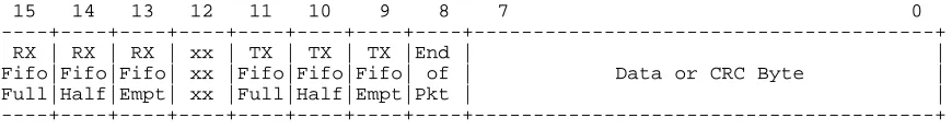
6.2. Receiver Data Register
The receiver data register, figure 7, is the read-port of a 4K by 9-bit FIFO. On the T1 line side of the FIFO, incoming data bits are shifted into an 8-bit register and then written in parallel into the write-port of the FIFO (see figure 11). One byte of receiver status, figure 8, is written into the FIFO after the last data byte of a packet. This receiver status byte is distinguished from the data bytes by the ninth bit of the FIFO, which appears as RxData.PktEnd. If PktEnd is zero, then bits 7..0 are a data byte, otherwise they are the receiver status applying to the previously read data bytes. The last four bytes before the receiver status are the packet’s CRC, and they should be discarded by software.
15 14 13 12 11 10 9 8 7 0 +----+----+----+----+----+----+----+----+---+ | RX | RX | RX | xx | TX | TX | TX |End | | |Fifo|Fifo|Fifo| xx |Fifo|Fifo|Fifo| of | Data or CRC Byte | |Full|Half|Empt| xx |Full|Half|Empt|Pkt | | +----+----+----+----+----+----+----+----+---+
Bits 31..16: no connection
Bits 15..9: Rx and Tx FIFO status
See the description in Control/Status Register. Bit 8 - End of Packet
One if bits 7..0 is Ending Status Zero if bits 7..0 is a Data byte. Bits 7..0: Data or CRC Byte
A data byte; the last four bytes before End Of Pkt are CRC bytes.
Figure 7: Receiver Data Register (RxData)
During operating system initialization, the device driver must synchronize with the adapter. The receiver runs all the time, and attempts to write packet bytes into the FIFO even if software isn’t servicing the adapter. When a device driver first starts up, it is likely to find that the receiver FIFO has overflowed and is full of stale packet fragments. These bogus fragments must be flushed until the FIFO is empty and a good receiver status has been read.
Efficient transfer of data from the receiver to main memory depends on minimizing I/O read references to the adapter, which take 10 cycles. Ideally the ratio of I/O reads to data bytes moved is slightly greater than one but much less than two. The FIFO status bits in the receiver data register reflect the state of the FIFO including the effect of the current read operation. If
RxData.FifoEmpty, is true then bits 7..0 are the last data byte available at the instant the read was happening, and the FIFO status bits in the CSR should be checked before reading the data register again. Do not read the receiver data register whencsr.RxFifoEmptyis true.
15 14 13 12 11 10 9 8 7 6 5 4 3 2 1 0 +----+----+----+----+----+----+----+----+----+----+----+----+----+----+----+----+ | RX | RX | RX | xx | TX | TX | TX |End |Loss|Loss|Loss| | | |Fifo| | |Fifo|Fifo|Fifo| xx |Fifo|Fifo|Fifo| of | of | of | of | 0 | 0 |Abrt|Over|Bad | |Full|Half|Empt| xx |Full|Half|Empt|Pkt |Sgnl|Fram|Data| | | |Flow|CRC | +----+----+----+----+----+----+----+----+----+----+----+----+----+----+----+----+
Bits 31..16: no connection
Bits 15..9: Rx and Tx FIFO status
See the description in Control/Status Register. Bit 8 - End of Packet
One if bits 7..0 is Ending Status. Zero if bits 7..0 is a Data byte. Bit 7 - Loss of Signal
Zero if the receiver sees a legal T1 signal. Bit 6 - Loss of Frame
Zero if the receiver is locked to D4 framing pattern. Bit 5 - Loss of Data
Zero if the packet is a multiple of eight bits; one if bits lost/added. Bit 4 - zero
Bit 3 - zero Bit 2 - Abort
One if the packet ended in an HDLC abort. Bit 1 - FIFO Overflow
One if the receiver wanted to write a byte but the FIFO was full. Bit 0 - Bad CRC
One if the Cyclic Redundancy Checksum is not correct.
The correct receiver status for a packet is bits 7..0 all zeros:
•LossOfSignalis one if the T1 signal did not contain sufficient pulses to keep the clock recovery circuit functioning. If no pulse is received in 32 consecutive bit cells thenLossOfSignalgoes to one, terminating any packet in progress.
•LossOfFrameis one if the T1 signal did not contain the D4 framing pattern. The frame detector will tolerate up to two incorrect bits out of 12 consecutive frame bits. If the receiver loses the framing pattern thenLossOfFramegoes to one, terminat-ing any packet in progress.
•LossOfData is one if the number of bits between HDLC flags, after deleting stuffed bits, was not evenly divisible by eight. If the remainder is non-zero then bits have been added or dropped from the data stream.
•Abort is one if a packet ended with an HDLC abort. Packets normally begin and end with HDLC flags, (01111110). If the T1 circuit dies (no more pulses), then the receiver will see all ones, which is an HDLC abort.
•FifoOverflow is one if the receiver wanted to write the FIFO, but it was full. The data is lost, but the occurance of the error is remembered as a receiver status bit.
FifoOverflow is cleared after successfully writing a receiver status (including theFifoOverflowerror bit) into the FIFO.
•BadCRC is one if the Cyclic Redundancy Checksum on the packet was incorrect. The last four bytes of a packet are a 32-bit CRC appended by the transmitter. If a bit is inverted, added or dropped between transmitter and receiver then the CRC will be bad at the receiver with very high probability.
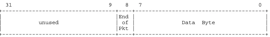
6.3. Transmitter Data Register
The transmitter data register, figure 9, is the write-port of a 4K by 9-bit FIFO. On the T1 line side of the FIFO, data bytes are read from the read-port of the FIFO and loaded into a shift register (see figure 13). The last byte of a transmitter packet is indicated by setting
TxData.EndOfPkt, which becomes the ninth bit in the FIFO. When this byte comes out the other end of the FIFO, the transmitter appends the checksum and generates the ending HDLC flag.
Note that a receiver packet ends with a status byte with the ninth bit set, but a transmitter packet ends with a data byte with the ninth bit set. The transmitter hardware generates and appends the CRC without software help, and the receiver hardware checks but does not delete the CRC, which the software must do.
If TxStart is one, the transmitter stops sending flags and starts reading and sending bytes from the FIFO. TxStartis asserted by settingTxData.EndOfPktorcsr.TxStart. The transmitter hardware clearsTxStartwithin 8 bit times, or about 5 microseconds. IfTxStart
is one but the FIFO is empty, then the transmitter simply clearsTxStartand continues to send flags.
31 9 8 7 0 +---+----+---+
| |End | |
| unused | of | Data Byte |
| |Pkt | |
+---+----+---+ Bits 31..9: no connection
Bit 8 - End of Packet
One if bits 7..0 are the last byte of a transmitter packet. Zero if bits 7..0 are a data byte except the last.
Bits 7..0: Data Byte A data byte.
Figure 9: Transmitter Data Register (TxData)
with bit 8 set) it appends 4 bytes of CRC, sets csr.TxIntReq and finally goes idle sending HDLC flags.
It is not possible to send back-to-back packets using the simple strategy of writing one packet into the FIFO and then waiting for the transmitter to interrupt. The transmitter will be idle for the time it takes to service the interrupt and load the next packet into the FIFO. To send back-to-back packets, software must write the next packet into the FIFO while the transmitter reads the current packet out of the FIFO.
Using the FIFO to double-buffer packets means that a pair of packets must fit into the 4 Kbyte FIFO. If no packet is longer than 2 Kbytes then this strategy works. The software writes the first packet into the FIFO, then waits forcsr.TxStartto go false, then writes the next packet into the FIFO, and so on. Software may only write one extra packet into the FIFO, even if more packets would fit, becauseTxStartis a single bit and not a counter.
Efficient transfer of data from main memory to the transmitter depends on minimizing I/O references to the adapter. Ideally the ratio of I/O writes to data bytes moved is slightly greater than one but much less than two. Do not write the transmitter data register when
csr.TxFifoFull is true. If the double-buffered strategy is used then the FIFO status bits don’t have to be checked in the data transfer loop.
csr.TxUnderflow is set if the transmitter attempts to read a byte from the FIFO but the FIFO is empty. The transmitter sends an HDLC abort without sending a CRC and then goes idle sending flags. This should never happen because the transmitter is never started until an entire packet is in the FIFO, but sometimes cosmic rays do funny things.
If the transmitter gets "stuck" in idle with bytes in the FIFO, software can unstick it by setting
csr.txStart. This wakes up the transmitter without writing any more bytes into the FIFO and causes it to read from the FIFO. This must be repeated until the FIFO runs dry. In any case, some packet fragments will be transmitted.
6.4. Option ROM
references are to 32-bit words. Consecutive ROM bytes are the least significant bytes of con-secutive 32-bit words.
The Option ROM has two parts: fixed-format configuration information and variable-format objects such as scripts, and executable code. System module firmware called the ROM Executive, or REX, can interpret the script objects and execute the code objects. Rather than reprogramming a ROM for each new version during development, REX can be directed to read an Option ROM image from an Ethernet boot server rather than from the ROM on the Option module. A Unix program written in Modula-2 generates the PROM programmer file and the net-bootable file.
REX loads a code object at a fixed address in memory and transfers control to it, passing a callback vector, an array of utility procedures that the code object can use to print messages on the console, etc. There is only one code object in this adapter’s Option ROM, a keyboard-driven diagnostic program written in Modula-2. The program is loaded in the cached kernel memory region because it runs about four times faster than uncached.
To use an Option ROM image booted from the net rather than the ROM on the adapter, register the file with a boot server, and use the undocumented REX command boot -D n 6/mop, wherenis the slot number of the adapter whose ROM is to be replaced (6/tftpworks too). REX commands invoking code objects will read this image rather than the adapter ROM until REX is reinitialized.
7. Diagnostic Program
The diagnostic program is started by typing t n to the REX prompt of >>, where n is the TurboChannel slot number of the adapter to be tested; i.e. t 0 starts the diagnostic program of an adapter in slot zero.
7.1. Program Variables
There are five program variables which can be set by command and influence the behavior of other commands:
•Length is a cardinal in the range 2..2048. If the Random program variable (see below) is true, then transmitted packets have random lengths between two and
Length bytes, otherwise transmitted packets have a constant length of Length
bytes.
•Random is a boolean variable. If true, then transmitted packets have random lengths and are filled with pseudo random numbers, otherwise packets have constant lengths equal totxLengthand are filled with the constant pattern (0 1...255). •DataCheck is a boolean variable. If it is true, then received packets will be
•LoopBack is a boolean variable. This value is loaded into csr.LoopBack
whenever the CSR is written. If true, the transmitter output is looped into the receiver input, all ones is transmitted to the T1 line, and packets arriving from the T1 line are ignored.
•Clockis a boolean variable. This value is loaded intocsr.txLclClkwhenever the CSR is written. If true, the transmitter uses a local crystal oscillator, otherwise it uses the clock recovered from the received signal.
7.2. Diagnostic Commands
The diagnostic is a keyboard-driven program which is used to debug adapters and test T1 circuits without the complication of going through an operating system. Typing "?" lists all of the commands; typing "help" prints a list of the commands along with one-line descriptions. To invoke a command, type an unambiguous initial substring terminated by a carriage return or space. To stop a running command, type any character.
•The Quit and Exit commands leave the adapter diagnostic program and return to the ROM Executive.
•The Test command transmits and receives packets continuously. Test is terminated by typing any character. For every 10 good packets received, a "!" is printed. Bad transmit and receive status values are printed and counted. At the end of the test, the number of good and bad transmit and receive packets is printed. This command is simply TxTest and RxTest (see below) called in a loop.
•The TxTest command transmits packets continuously. TxTest is teminated by typing any character. For every 10 good packets transmitted, a "!" is printed. If
csr.txUnderFlow is true, the CSR is printed and the packet is counted as bad. At the end of the test, the number of good and bad packets is printed. Packet length and contents are controlled by theLengthandRandomprogram variables.
•The RxTest command receives packets continuously. RxTest is terminated by typing any character. For every 10 good packets received, a "!" is printed. If any error bits are set, the receiver status is printed and the packet is counted as bad. At the end of the test, the number of good and bad packets is printed. Packet contents are checked if theDataCheckprogram variable is true.
•The Echo command transmits any packets received. Echo is terminated by typing any character. For every 10 good packets echoed, a "!" is printed. Bad transmit and receive status values are printed. At the end of the test, the number of packets echoed is printed.
•The Watch command prints all packets received. Watch is terminated by typing any character. Each packet begins on a new line preceded by "data=". Packet data bytes are printed as two character hex values separated by spaces. Each packet ends by printing the receiver status on a new line.
•The Reset command attempts to put the adapter in an idle state. It clears
csr.rxIntReq, csr.txIntReq, and csr.txUnderflow. It sets
RxFIFO, so if csr.LoopBack is false and packets are arriving, the status after a reset may still showcsr.rxIntReqtrue andcsr.rxFifoEmptyfalse.
•The Status command prints the contents of the Control/Status Register (CSR) as a hex number and as named fields.
•The Length command sets the Length program variable. Acceptable values are between 2 and 2048.
•The Random command toggles theRandomprogram variable. Transmitted packets are random length and filled with random data ifRandomis true.
•The DataCheck command toggles the DataCheck program variable. Data in received packets are checked ifDataCheckis true.
•The Loop command toggles the LoopBack program variable. Transmitter output is looped to receiver input ifLoopBackis true. FrameSyncandCarrierLEDs should light whenLoopBackis set.
•The Clock command toggles theClockprogram variable. The transmitter uses the local crystal oscillator ifClockis true.
•The Speed command transmits back-to-back packets and measures bits per second and packets per second. Speed is terminated by typing any character. The length of the transmitted packets is controlled by the Lengthprogram variable. The data in the transmitted packets is the constant pattern (0 1...255). This data pattern will cause HDLC bit-stuffing to occur, so the bit/sec reported by the command will be somewhat less than the maximum rate of 1.536 Mb/s. Five overhead bytes are added to each packet when calculating the bit rate (one flag and four CRC bytes). The clock used for this test has a resolution of 1 second, so the accuracy increases with increasing test time. The speed test is a tight loop running on the bare hardware; your mileage may vary when running the adaptor through an operating system.
•The AbortTest command tests the HDLC abort generation and detection logic in the transmitter and receiver. AbortTest is terminated by typing any character. At the end of the test the number of good and bad results is printed. The transmitter is forced to generate an HDLC abort by deliberately causing a transmitter FIFO under-flow: two bytes are written into the FIFO and then the transmitter is started by set-ting csr.txStart instead of setting the ninth bit of the last data byte. If
RxStatus.abortis true, then everything is working.
•The ScopeLoop command continuously reads the control and status register. ScopeLoop is terminated by typing any character. This command generates steady oscilloscope pictures for debugging the TurboChannel control logic.
7.3. Using the Commands
By looping a T1 circuit at various points and using the diagnostic commands, a number of questions about the link and adapters can be answered.
•Does-the-Adapter-Work Test. A quick and thorough way to test the adapter is to set
variables have been changed from their initial values, Test will transmit packets of randomly varying length filled with random numbers and check the data in the returning packets. At the beginning of the test, a few bad statuses may be reported as the software synchronizes with the hardware. At the end of the test, the number of good packets received may not exactly match the number of good packets sent. •Does-the-T1-Circuit-Work Test. Rather than looping the adapter internally, there
are usually several ways to loop the T1 circuit itself. Once the circuit has been looped externally, Test can be run without setting csr.LoopBack. Setting the loopback switch on the CSU will test all of the adapter, the cable from the adapter to the CSU, and most of the CSU. CSUs also usually have a switch which will send a special signal down the T1 circuit and loop the far-end CSU. Doing this will test all of the adapter, near-end CSU, T1 circuit, and most of the far-end CSU.
•Two-Way Test. To test both adapters and the entire T1 circuit, run the Echo
com-mand on one adapter and run Test on the other adapter. In this case
csr.LoopBackshould be false at both adapters.
•One-Way Test. If Test fails, it isn’t always obvious whether the receiver or the
transmitter is having problems. These can be tested separately by using a known-good adapter. Connect the two adapters with a null-modem cable, run RxTest on the good adapter and run TxTest on bad adapter. If the test fails, the problem is a bad transmitter. Similarly, run TxTest on the good adapter and RxTest on the bad adapt-er. If the test fails, the problem is a bad receivadapt-er. This technique can also be used to isolate a failure in one direction of a T1 circuit.
•Is-Anybody-Out-There Test. Often when installing a new T1 circuit, it is useful to
know if any packet is being received. Also, when debugging new operating system software, it is sometimes useful to get an indendent opinion on whether packets are being transmitted and if they are well-formed. The Watch command will print out anything that is not an HDLC flag, including line noise, test patterns generated by the telephone company, and malformed packets.
8. Technical Description
The Line Interface Unit, or LIU, contains analog black magic: delay-line clock recovery, a jitter attenuator, and an output pulse shaper. The LIU recovers the clock from the incoming pulse stream with a digital phase locked loop containing a 13-tap variable delay line. Jitter in the recovered clock is attenuated by means of a 32-bit FIFO and a variable crystal oscillator. Output pulses are formed by a slew-rate controlled fast digital-to-analog converter generating a piecewise linear approximation of a wire-length dependent pulse shape.
The Transmitter and Receiver Finite State Machines (TxFSM and RxFSM), use 8Kx8 regis-tered PROMs. The RxFSM has eight states and 21 outputs, and the TxFSM has seven states and 23 outputs; each machine uses three PROMs. The FSMs clock about eight times per T1 bit cell; a T1 bit is 648 ns wide and the FSMs clock every 80 ns. This gives plenty of cycles between each bit during which to shift shift registers, count counters, test for underflow, etc. 1.5 Mb/s is loafing: things can be done by brute force in TTL without pushing any speed limits.
handle several packets during one interrupt context switch when the adapter is busy. They also make it easy to handle back-to-back packets (separated by only one HDLC flag) without heoric efforts by the device driver. Careful thought was given to minimizing the number of instruction cycles per byte transferred. By returning the receiver FIFO status when a data byte is read, an extra I/O read of the CSR is avoided inside the copy loop; similarly, an extra I/O read of the CSR is not necessary in the transmitter copy loop.
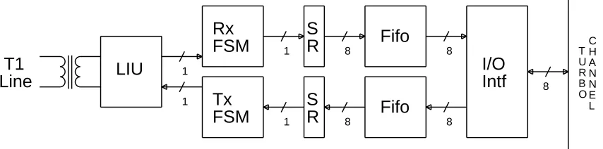
8.1. Data Path
Figure 10 is a block diagram of the data paths in the adapter. Starting at the T1 line, pulses are coupled through a transformer into the LIU. The LIU derives a clock from the incoming pulses and supplies data bits to the RxFSM. The RxFSM deletes the T1 frame bits and the HDLC stuff bits and accumulates the data bits in a Shift Register, SR. When the SR is full, the RxFSM writes the data byte into the FIFO; it can also parallel load the SR with receiver status and write that into the FIFO. Data bytes flow out of the FIFO, through the I/O Interface and onto the TurboChannel when a program executes a load instruction whose effective address falls within the adapter’s 4 MByte space.
I/O Intf
T U R B O C H A N N E L 8
T1 Line
1 1
S
R Fifo Rx
FSM 1 8 8
Fifo Tx
FSM 1 8 8
[image:20.612.115.542.320.426.2]S R LIU
Figure 10: Data Paths in the Adapter
The data path for the transmitter is symmetric with the receiver. Data bytes flow over the TurboChannel, through the I/O interface and into the FIFO when a program executes a store instruction whose effective address falls within the adapater’s address space. The TxFSM reads bytes from the FIFO loads them into the SR, inserts T1 frame bits, HDLC stuff bits and CRC bits, and feeds the resulting bit stream to the LIU. The LIU generates the positive and negative pulses and drives the DSX-1 interface through a transformer.
8.2. Receiver
LIU
8 Cnt
5 Cnt 3
1 1
2 T1 LINE
2 192 Cnt
4
8Kx24 proms
TURBO CHANNEL
CRC 32
12 SR 8 SR 8
Frame Rom
[image:21.612.148.437.74.258.2]Fifo
Figure 11: Block Diagram of the Receiver
T1 frame synchronization uses 12SR, 192Cnt, and FrameRom; the object is to make 192Cnt underflow when a frame bit is expected. 8Cnt and 5Cnt are also used since data bytes are not accumulated and stuff bits are not deleted while trying to locate the framing pattern. The first step is to zero 12SR and preset 192Cnt, 8Cnt and 5Cnt; the next bit to emerge from the LIU is tentatively assumed to be a frame bit and it is shifted into 12SR. The FrameRom looks at 12SR and renders a judgement as to whether it contains the framing pattern (100011011100) in one of its 12 rotations:
•No.12SR does not contain anything remotely like a framing pattern.
•Maybe. 12SR contains a framing pattern up to the last 1-bit (recall that 12SR is initialized to 0s and less than 12 frame bits may be in the register).
•Error.12SR contains a framing pattern with one or two bits in error. •Yes.12SR contains a framing pattern exactly.
If after shifting a potential frame bit into 12SR, FrameRom says Noor Errorthen move over one bit in the stream and assume that it is a frame bit by going back to step one. As long as FrameRom saysMaybeorYes, continue shifting every 193rd bit into 12SR, and counting 8Cnt and 5Cnt; when they both underflow, 40 good frame bits have been seen so csr.FrameSync
132 844 Error
50
50
50
50
50 No
12
12
12
12
12 0
1 2 3 4
Bad Yes Maybe
0 2352 3591
[image:22.612.218.437.80.213.2]4034 3902 3190 1682 443
Figure 12: Loss-of-frame lock threshold
8.3. Transmitter
Figure 13 is a block diagram of the transmitter; arrows show the path of the data bits. Note how similar it is to the receiver; the major difference is that less machinery is needed to transmit the frame pattern than to receive it. The Mux generates the framing pattern from a modulo-12 counter, as well as steering data, CRC and stuff bits to the LIU. Mux feeds back the value of the outgoing bit to TxFSM so that it can count bits for HDLC stuffing. The signal from LIU to TxFSM is the transmitter clock, informing it that a bit has been accepted and the next bit should be set up. The signal from the FIFO to the RxFSM is fifoEmpty; the signal from 8SR is En-dOfPkt (ninth fifo bit).
8Kx24 proms
csr.TxStart
1
1
T1 LINE
1 5 Cnt 8 Cnt
Fifo 8 SR
CRC 32 Mux LIU
1
TURBO CHANNEL 1
1 1 1 5
8 1
[image:22.612.130.526.427.657.2]192 Cnt
9. Design Choices
Why use Crystal Semi’s LIU? At least thirteen companies make Line Interface Unit ICs;
some just second-source others, some make separate receiver and transmitter chips, and some partition functions in odd ways. Figure 14 compares the nine LIU chips that looked promising.
Tech = chip technology; RClk = Receiver clock recovery technique; Comp = external com-ponents;LOS= reports loss of signal;Loop= loopback capability;BPV= reports bipolar viola-tions;Puls= transmitter pulse shaping;Jitt= attenuates jitter.
[image:23.612.84.501.190.409.2]78P233 R8069 T5683 Comp None No No No No No No No No No No No No No No No No No No No No RC C Bip Bip Bip Rockwell Dallas Company AT&T Crystal Exar Siemens TI TCM2203 PEB2235 DS2185 CS61574 LC1046 Chip Tech CMos CMos CMos NMos CMos CMos Tank APLL DPLL APLL DPLL Tank APLL DDly APLL RClk Xtal RLC Xtal Xtal Xtal RLC Yes Yes Yes Yes Yes Yes LOS BPV Yes Yes Yes Yes Yes Yes Yes Yes Yes Loop Puls Yes Yes Yes Yes Yes Yes Yes Yes Jitt xxx xxx EFB7332 SilSys Thomson
Figure 14: Line Interface Unit ICs
Jitter attenuation was the deciding factor in choosing an LIU. When the transmitter clock is derived from the received pulse stream, jitter must be eliminated or it may build up to unaccept-able levels by the time it gets back to the far end. The Rockwell chip was new and only avail-able for sampling, and its input jitter tolerance was half that of the Crystal chip; the Dallas chip was a receiver only (but nicely done). The TI and Exar chips were rather old designs requiring many external components; the Silicon Systems chip required fewer components. The Mostek and Siemans chips were European designs using oversampling digital phase locked loops and no external components except crystals; both of them looked very good and would have been con-tenders if they had contained jitter attenuators. The AT&T chip was designed by the people who invented T1, but they didn’t include a jitter attenuator. (In defense of LIUs without jitter at-tenuation, it is often done elsewhere in a design.) The Crystal Semiconductor LIU did every-thing required and only a few every-things not required (output driver monitoring and serial control interface).
Rather than doing extensive simulation before making the printed circuit board, the adapter was designed to be easy to modify by reprogramming the ROMs and PALs; every reprogrammable part was changed at least once during debugging and two wires were added to unused inputs. The added wires were the result of misunderstanding the operation of two ICs, so the behavioral models would have been wrong and the errors would not have been caught during simulation. The receiver frame sync algorithm was simulated, and it helped, but several changes were neces-sary when a real T1D4 signal was seen for the first time. Experience using the adapter suggested several changes to the software interface, which were easy to make by reprogramming. A programmable gate array, such as those made by Xilinx, is an attractive alternative to partition-ing the design among a number of smaller chips.
Why include the DSU function rather than using an external DSU/CSU? Integrating the
DSU with the HDLC logic resulted in a very compact design. An external DSU implies an electrical interface, such as EIA422/423/449 or V.35, between the HDLC logic and the DSU, and the ability to run at fractional T1 speeds. While designing a general-purpose synchronous serial adapter is a worthy goal, the goal here was to build a single-purpose T1 adapter. Multiprotocol routers exist and the cost of T1 circuits is plummeting, so the need to split a T1 circuit between two routers implementing different protocols, or to save money with a fractional T1 circuit will fade. Integrating the CSU function into the adapter would have been going too far; a CSU’s interface is not as flexible as DSX-1.
Why implement framing rather than using a framer chip? Designing the frame recognizer
was an intellectual challenge. Several companies make VLSI chips that do D4 and ESF framing, plus many features for treating a T1 circuit as 24 voice channels. Other than framing, these features are not needed, are sometimes hard to disable, and are always complicated to configure. Getting bits past these features without mangling is like walking through a mine field.
Why D4 framing rather than ESF? ESF is very complicated; D4 is much simpler to
imple-ment. Most T1 circuits use D4 framing; a circuit with ESF (and usually B8ZS also) is a special-order item not available everywhere. If ESF is absolutely required for some reason, then there are CSUs which can speak D4 on the customer side and ESF on the telco side; an EIA232 ter-minal port on the CSU gives access to the ESF features.
Why implement HDLC rather than using a serial chip? Many companies make VLSI chips
that implement HDLC, from simple serial chips to complicated protocol chips that interpret the address and control fields. Like the T1 framer chips, HDLC chips are usually quite complex to configure, sometimes even including scatter/gather DMA. Transporting unreliable datagrams between routers requires only the most basic aspects of HDLC; the rest gets in the way.
Why programmed I/O rather than DMA? There was no room on the printed circuit board. A
Why 32-bit CRC rather than 16-bit CRC? The error detecting ability of a 16-bit CRC decreases beyond a packet size of about 4K bits; the maximum packet size of this adapter is 16K bits. Ethernet, which has a maximum packet size of about 12K bits, uses a 32-bit CRC recom-mended in HDLC [19]. This adapter uses the same CRC because packets moving through the adapter probably come from or are destined for an Ethernet, so they should get the same level of protection.
Instead of hand-crafting D4 framing and HDLC using a few simple FSMs, a T1 adapter could be designed using a T1 framer chip connected to an HDLC chip which DMAed into an on-board buffer ram, similar to the design of DEC’s PMAD-AA Ethernet adapter. Such a design would not require understanding the details of T1 or HDLC. It would certainly be more complex to program and there would be more ways to lose performance, but it is a workable approach.
10. Bugs
If the last five bits of the CRC were ones, then the TxFSM failed to insert a stuff bit. The receiver took the first bit of the ending flag as a stuff bit, and things went downhill from there. This turns out to be a common error in HDLC implementations; several standards documents mention that a stuff bit may be required after the last CRC bit and before the closing flag. One extra state was added to the TxFSM to fix this bug. IP protocols managed to work despite the fact that about 3 percent of the packets were being discarded due to bad receiver status.
The receiver’s frame synchronizer would falsely lock onto the transmitter’s HDLC flag pat-tern 25 percent of the time. If a zero bit in an HDLC flag was picked as a possible frame bit, then on an idle link with all flags, every 193rd bit after that would also be a zero, the FrameRom would sayMaybe 40 times, and frame synchronization would be falsely declared. Simulations of the frame sync algorithm used random data and did not find this problem. A two-line change to the RxFSM fixed this bug.
The TurboChannel clock is used to clock the FSMs in the adapter. For a maximum-speed 25 MHz TurboChannel, the clock is divided by two giving an 80 ns period, or about eight cycles per T1 bit. For a minimum-speed 12.5 Mhz TurboChannel, dividing by two results in four cycles per bit, which is not enough. The clock division is done in a PAL, so the quick fix is to use a different PAL for fast and slow systems; the long-term fix is to make this a CSR bit.
Several companies make routers that use T1 lines and it would be good if they could inter-operate with this adapter. They use HDLC chips (such as the 8530) through a V.35 interface to a DSU/CSU which handles framing and clocking. Most HDLC chips only implement 16-bit CRCs. The CRC chips used in this design were advertised to implement both 16- and 32-bit polynomials, but 16-bit polynomial checking only works if the CRC bits are inverted before be-ing shifted into the chip (it does the right thbe-ing for 32 bits). By reprogrammbe-ing PROMs to invoke hidden features, the adapter can be made to generate packets with correct 16-bit CRCs, but it can’t check the 16-bit CRC of an incoming packet (software can do it fairly inexpensively).
had to be cut and a wire added; the adapter talked to itself or others of its kind just fine the old way.
The RxFSM was generating FIFO write pulses when the FIFO was full. The data sheet im-plied that this was harmless, but by pounding on the adapter for about six hours in a particular way, the FIFO could be driven into a bad state. FifoWrite was already passing through a PAL for other reasons, so it was simple to quash it if FifoFull was true; this required adding a wire from FifoFull to an unused input on the PAL. The FifoOverflow logic had to be reprogrammed as a side effect.
11. Acknowledgements
12. References
[1] American National Standards Institute.
Synchronization Interface Standards for Digital Networks.
American National Standard T1.101-1987, ANSI, December, 1986.
[2] American National Standards Institute. Digital Hierarchy - Electrical Interfaces.
American National Standard T1.102-1987, ANSI, August, 1987.
[3] American National Standards Institute.
Carrier-to-Customer Installation--DS1 Metallic Interface. American National Standard T1.403-1989, ANSI, 1989.
[4] American National Standards Institute.
Advanced Data Communication Control Procedures (ADCCP). American National Standard X3.66-1979, ANSI, January, 1979.
[5] American Telephone and Telegraph Company. High Capacity Terrestrial Digital Service.
Technical Reference 41451, AT&T, January, 1983.
[6] American Telephone and Telegraph Company. Digital Channel Bank Requirements and Objectives. Technical Reference 43801, AT&T, November, 1982.
[7] American Telephone and Telegraph Company. Extended Superframe Format.
Technical Reference 54016, AT&T, May, 1986.
[8] American Telephone and Telegraph Company. Digital Synchronization Network Plan.
Technical Reference 60110, AT&T, December, 1983.
[9] American Telephone and Telegraph Company.
ACCUNET T1.5 Service Description and Interface Specifications. Technical Reference 62411, AT&T, October, 1985.
[10] American Telephone and Telegraph Company.
Interconnection Specification for Digital Cross-Connects. Compatibility Bulletin 119, AT&T, October, 1979.
[11] Bell Communications Research.
Asynchronous Digital Multiplexes Requirements and Objectives. Technical Reference TSY-000009, BellCore, May, 1986.
[12] Bell Communications Research.
Synchronous DS3 Add-Drop Multiplex (ADM 3/X) Requirements and Objectives. Technical Reference TSY-000010, BellCore, February, 1988.
[13] Bell Communications Research.
[14] Bell Communications Research.
Synchronous Optical Network (SONET) Transport Systems: Common Generic Criteria. Technical Reference TSY-000253, BellCore, September, 1989.
[15] International Telegraph and Telephone Consultative Committee. Digital Hierarchy of Bit Rates.
Recommendation G.702, CCITT, November, 1988.
[16] International Telegraph and Telephone Consultative Committee. Physical/Electrical Characteristics of Hierarchical Digital Interfaces. Recommendation G.703, CCITT, November, 1988.
[17] International Telegraph and Telephone Consultative Committee.
Functional Characteristics of Interfaces Associated with Network Nodes. Recommendation G.704, CCITT, November, 1988.
[18] International Telegraph and Telephone Consultative Committee.
The control of jitter and wander within digital networks which are based on the 1544 kbit/s hierarchy.
Recommendation G.824, CCITT, November, 1988.
[19] International Standards Organization. HDLC Frame structure.
International Standard 3309, ISO, 197?
[20] C. Davis.
An Experimental Pulse Code Modulation system for Short-Haul Trunks. Bell System Technical Journal 41(1):1-24, January, 1962.
[21] J. Mayo.
A Bipolar Repeater for Pulse Code Signals.
Bell System Technical Journal 41(1):25-97, January, 1962.
[22] M. Aaron.
PCM Transmission in the Exchange Plant.
Bell System Technical Journal 41(1):99-141, January, 1962.
[23] K. Fultz and D. Penick. The T1 Carrier System.
Bell System Technical Journal 44(5):1405-1451, September, 1965.
[24] A. Duttweiler. Waiting Time Jitter.
Bell System Technical Journal 51(1):165-207, January, 1972.
[25] C. Byrne, R. Karafin and D. Robinson.
Systematic Jitter in a Chain of Digital Regenerators.
Bell System Technical Journal 42(6):2679-2714, November, 1963.
[26] International Business Machines Corporation. Binary Synchronous Communications.
[27] International Business Machines Corporation. IBM Synchronous Data Link Control.
General Information GA-27-3093, IBM, 197?
[28] R. Donnan and J. Kersey.
Sunchronous Data Link Control: A Perspective. IBM Systems Journal 13:140-162, May, 1974.
[29] Digital Equipment Corporation.
TurboChannel Hardware Specification. Document EK-369AA-OD, DEC, 1991.
[30] Digital Equipment Corporation.
TurboChannel Firmware Specification. Document EK-TCAAD-FS, DEC, 1991.
WRL Research Reports
‘‘Titan System Manual.’’ ‘‘MultiTitan: Four Architecture Papers.’’
Michael J. K. Nielsen. Norman P. Jouppi, Jeremy Dion, David Boggs, Mich-WRL Research Report 86/1, September 1986. ael J. K. Nielsen.
WRL Research Report 87/8, April 1988. ‘‘Global Register Allocation at Link Time.’’
David W. Wall. ‘‘Fast Printed Circuit Board Routing.’’ WRL Research Report 86/3, October 1986. Jeremy Dion.
WRL Research Report 88/1, March 1988. ‘‘Optimal Finned Heat Sinks.’’
William R. Hamburgen. ‘‘Compacting Garbage Collection with Ambiguous WRL Research Report 86/4, October 1986. Roots.’’
Joel F. Bartlett.
‘‘The Mahler Experience: Using an Intermediate WRL Research Report 88/2, February 1988. Language as the Machine Description.’’
David W. Wall and Michael L. Powell. ‘‘The Experimental Literature of The Internet: An WRL Research Report 87/1, August 1987. Annotated Bibliography.’’
Jeffrey C. Mogul.
‘‘The Packet Filter: An Efficient Mechanism for WRL Research Report 88/3, August 1988. User-level Network Code.’’
Jeffrey C. Mogul, Richard F. Rashid, Michael ‘‘Measured Capacity of an Ethernet: Myths and
J. Accetta. Reality.’’
WRL Research Report 87/2, November 1987. David R. Boggs, Jeffrey C. Mogul, Christopher A. Kent.
‘‘Fragmentation Considered Harmful.’’ WRL Research Report 88/4, September 1988. Christopher A. Kent, Jeffrey C. Mogul.
WRL Research Report 87/3, December 1987. ‘‘Visa Protocols for Controlling Inter-Organizational Datagram Flow: Extended Description.’’
‘‘Cache Coherence in Distributed Systems.’’ Deborah Estrin, Jeffrey C. Mogul, Gene Tsudik,
Christopher A. Kent. Kamaljit Anand.
WRL Research Report 87/4, December 1987. WRL Research Report 88/5, December 1988.
‘‘Register Windows vs. Register Allocation.’’ ‘‘SCHEME->C A Portable Scheme-to-C Compiler.’’
David W. Wall. Joel F. Bartlett.
WRL Research Report 87/5, December 1987. WRL Research Report 89/1, January 1989.
‘‘Editing Graphical Objects Using Procedural ‘‘Optimal Group Distribution in Carry-Skip
Ad-Representations.’’ ders.’’
Paul J. Asente. Silvio Turrini.
WRL Research Report 87/6, November 1987. WRL Research Report 89/2, February 1989.
‘‘The USENET Cookbook: an Experiment in ‘‘Precise Robotic Paste Dot Dispensing.’’ Electronic Publication.’’ William R. Hamburgen.
Brian K. Reid. WRL Research Report 89/3, February 1989.
‘‘Simple and Flexible Datagram Access Controls for ‘‘Link-Time Code Modification.’’
Unix-based Gateways.’’ David W. Wall.
Jeffrey C. Mogul. WRL Research Report 89/17, September 1989. WRL Research Report 89/4, March 1989.
‘‘Noise Issues in the ECL Circuit Family.’’ Jeffrey Y.F. Tang and J. Leon Yang. ‘‘Spritely NFS: Implementation and Performance of
WRL Research Report 90/1, January 1990. Cache-Consistency Protocols.’’
V. Srinivasan and Jeffrey C. Mogul.
‘‘Efficient Generation of Test Patterns Using WRL Research Report 89/5, May 1989.
Boolean Satisfiablilty.’’ Tracy Larrabee.
‘‘Available Instruction-Level Parallelism for
Super-WRL Research Report 90/2, February 1990. scalar and Superpipelined Machines.’’
Norman P. Jouppi and David W. Wall.
‘‘Two Papers on Test Pattern Generation.’’ WRL Research Report 89/7, July 1989.
Tracy Larrabee.
WRL Research Report 90/3, March 1990. ‘‘A Unified Vector/Scalar Floating-Point
Architec-ture.’’
‘‘Virtual Memory vs. The File System.’’ Norman P. Jouppi, Jonathan Bertoni, and David
Michael N. Nelson. W. Wall.
WRL Research Report 90/4, March 1990. WRL Research Report 89/8, July 1989.
‘‘Efficient Use of Workstations for Passive Monitor-‘‘Architectural and Organizational Tradeoffs in the
ing of Local Area Networks.’’ Design of the MultiTitan CPU.’’
Jeffrey C. Mogul. Norman P. Jouppi.
WRL Research Report 90/5, July 1990. WRL Research Report 89/9, July 1989.
‘‘A One-Dimensional Thermal Model for the VAX ‘‘Integration and Packaging Plateaus of Processor
9000 Multi Chip Units.’’ Performance.’’
John S. Fitch. Norman P. Jouppi.
WRL Research Report 90/6, July 1990. WRL Research Report 89/10, July 1989.
‘‘1990 DECWRL/Livermore Magic Release.’’ ‘‘A 20-MIPS Sustained 32-bit CMOS
Microproces-Robert N. Mayo, Michael H. Arnold, Walter S. Scott, sor with High Ratio of Sustained to Peak
Perfor-Don Stark, Gordon T. Hamachi. mance.’’
WRL Research Report 90/7, September 1990. Norman P. Jouppi and Jeffrey Y. F. Tang.
WRL Research Report 89/11, July 1989.
‘‘Pool Boiling Enhancement Techniques for Water at Low Pressure.’’
‘‘The Distribution of Instruction-Level and Machine
Wade R. McGillis, John S. Fitch, William Parallelism and Its Effect on Performance.’’
R. Hamburgen, Van P. Carey. Norman P. Jouppi.
WRL Research Report 90/9, December 1990. WRL Research Report 89/13, July 1989.
‘‘Writing Fast X Servers for Dumb Color Frame Buf-‘‘Long Address Traces from RISC Machines:
fers.’’ Generation and Analysis.’’
Joel McCormack. Anita Borg, R.E.Kessler, Georgia Lazana, and David
WRL Research Report 91/1, February 1991. W. Wall.
‘‘Analysis of Power Supply Networks in VLSI Cir-cuits.’’
Don Stark.
WRL Research Report 91/3, April 1991.
‘‘TurboChannel T1 Adapter.’’ David Boggs.
WRL Research Report 91/4, April 1991.
‘‘Procedure Merging with Instruction Caches.’’ Scott McFarling.
WRL Research Report 91/5, March 1991.
‘‘Don’t Fidget with Widgets, Draw!.’’ Joel Bartlett.
WRL Research Report 91/6, May 1991.
‘‘Pool Boiling on Small Heat Dissipating Elements in Water at Subatmospheric Pressure.’’
Wade R. McGillis, John S. Fitch, William R. Hamburgen, Van P. Carey.
WRL Research Report 91/7, June 1991.
‘‘Incremental, Generational Mostly-Copying Gar-bage Collection in Uncooperative Environ-ments.’’
G. May Yip.
WRL Research Report 91/8, June 1991.
WRL Technical Notes
‘‘TCP/IP PrintServer: Print Server Protocol.’’ ‘‘Why Aren’t Operating Systems Getting Faster As Brian K. Reid and Christopher A. Kent. Fast As Hardware?’’
WRL Technical Note TN-4, September 1988. John Ousterhout.
WRL Technical Note TN-11, October 1989. ‘‘TCP/IP PrintServer: Server Architecture and
Im-plementation.’’ ‘‘Mostly-Copying Garbage Collection Picks Up
Christopher A. Kent. Generations and C++.’’
WRL Technical Note TN-7, November 1988. Joel F. Bartlett.
WRL Technical Note TN-12, October 1989. ‘‘Smart Code, Stupid Memory: A Fast X Server for a
Dumb Color Frame Buffer.’’ ‘‘Limits of Instruction-Level Parallelism.’’
Joel McCormack. David W. Wall.
‘‘The Effect of Context Switches on Cache Perfor-mance.’’
Jeffrey C. Mogul and Anita Borg.
WRL Technical Note TN-16, December 1990. ‘‘MTOOL: A Method For Detecting Memory
Bot-tlenecks.’’
Aaron Goldberg and John Hennessy.
WRL Technical Note TN-17, December 1990.
‘‘Predicting Program Behavior Using Real or Es-timated Profiles.’’
David W. Wall.
WRL Technical Note TN-18, December 1990.
‘‘Systems for Late Code Modification.’’ David W. Wall.