Common-mode Voltage Reduction for Matrix
Converters Using All Valid Switch States
Quanxue Guan,
Student Member, IEEE,
Patrick Wheeler,
Senior Member, IEEE,
Quansheng Guan,
Member, IEEE,
and Ping Yang
Member, IEEE,
Abstract—This paper presents a new space vector modulation (SVM) strategy for matrix converters to reduce the common-mode voltage (CMV). The reduction is achieved by using the switch configurations that connect each input phase to a different output phase, or the configurations that connect all the output phases to the input phase with minimum absolute voltage. These two types of configurations always produce lower peak CMV than the others, especially the former ones that result in zero CMV at the output side of matrix converters. In comparison with the existing SVM methods, this strategy has a very similar software overhead and calculation time. Simulation and experiment results are shown to validate the effectiveness of the proposed modulation method in reducing not only the peak value but also the root mean square value of the CMV.
Index Terms—Common-mode Voltage, Matrix Converters, Sin-gular Value Decomposition, Space Vector Modulation.
I. INTRODUCTION
T
HE matrix converter (MC) has been a promising power converter topology during the past decades [1], [2]. The main reason for this interest lies in the potential advantages of MCs, such as direct conversion, controllable input displace-ment factor, bi-directional power flow and high power density. The modulation algorithm is one of the important factors in determining the performance of MCs. The existing modulation algorithms for MCs are intrinsically based on the well-known pulse-width modulation (PWM) [3]. As a result of the PWM switching pattern, MC generates a series of staircase-like high frequency common-mode voltage (CMV) waveforms. Similar CMV also appears in three-phase inverters [4]–[6]. Large mag-nitude and high frequency variation of CMV, unfortunately, have been known as the root causes of early motor winding failure and machine bearing deterioration [7].Different methods have been reported to mitigate the detri-mental influences of the CMV for MCs. An intuitive idea is
Manuscript received August 23, 2014; revised July 08, 2015, September 18, 2015 and November 14, 2015; accepted January 05, 2016. Date of publication XXX.XX, 2016; date of current version January 20, 2016. This work was supported in part by the National Natural Science Foundation of China under Grant 61302058 and Grant 61431005, and in part by Guangzhou Elite Oversea Study Program under Grant JY201323.
Quanxue Guan is with the School of Electronic and Information Engineer-ing and School of Electric Power, South China University of Technology, Guangzhou, 510640, P.R.China (e-mail: [email protected]).
P. W. Wheeler is with the Department of Electrical and Electronic En-gineering, University of Nottingham, Nottingham, NG7 2RD, U.K. (e-mail: [email protected]).
Quansheng Guan is with the School of Electronic and Information Engineer-ing, South China University of Technology, Guangzhou, 510640, P.R.China (e-mail: [email protected]). Quansheng Guan is the corresponding author. Ping Yang is with the School of Electric Power, South China University of Technology, Guangzhou, 510640, P.R.China (e-mail: [email protected]).
using only the rotating vectors that correspond to the switch configurations with zero CMV in dual structure converters [8]– [16]. This technique has been applied to direct and indirect MC fed open-end winding AC drives to reduce or even eliminate the CMV. However, it is not considered in this paper owing to the increased costs and control complexities introduced by additional power semiconductor devices.
Methods exist that modify modulation strategies to reduce the magnitude of the CMV issues [17]–[30]. Since the CMV is brought about by the input voltages together with different switch configurations, it is preferable to choose those with low peak CMVs and low voltage transitions whenever possible. In the space vector modulation (SVM) algorithms for MCs [31]– [33], switch configurations are selected under the criterion of minimizing the switching count. Therefore, four active switch configurations and one zero switch configuration (ZSC) are selected in each sampling period. In order to reduce the CMV, two active vectors with opposite directions or three nearest-state vectors were chosen instead during the time intervals for the zero vectors in [17]–[23]. Unfortunately, these methods use more than five switch configurations in each sampling period, thus increase the switching power losses. Besides, the latter method can be applied only when the voltage transfer ratio (VTR) is larger than 0.667 [23]. When the VTR is smaller than 0.5, Hong-Hee Leeet al.also put forward several CMV-reduced strategies using two adjacent vectors with120◦-phase shift to reduce the duty cycles for zero vectors [20]–[25]. From the perspective of CMV reduction, however, it is unnecessary to exclude all ZSCs, because the CMV peak of the zero vector connecting to the input phase that is with the medium voltage value is lower than those of active vectors [26]–[30].
Note that for a three-phase-to-three-phase direct MC, the switch configurations that connect each input to one different output phase have zero CMV. The corresponding voltage vec-tors of these switch configurations have been often referred to as the “rotating vectors”. In this context, the perhaps more ap-propriate name is given for this type of switch configurations, i.e. “Orientation Switch Configuration” (OSC). Nevertheless, they are regarded to be trivial in the literature [31]–[33]. It is difficult to calculate their duty cycles and arrange them in the switching sequence [34]–[42]. For example, Yugo Tadano et al. tried to use these switch configurations though at the cost of complex switch pattern selection [39], [40]. Jordi Espina
Without the need of modulation, Rene Vargas et al. added a term in the quality function of the predictive model to suppress the CMV [43]–[46]. However, this method has a high computational overhead.
To use the OSCs in the modulation, we first investigate all valid switch configurations by applying the singular value de-composition (SVD) on their space vector representations [47]. The geometrical meaning of SVD can reveal how each switch configuration transforms a column vector between different reference frames. Thus, it provides an insight on the intrinsic properties of the switch configurations. These switch config-urations are then categorized into three types according to their SVD results. The relationships between different switch configurations are also found so that the OSCs can be used easily by equivalent decomposition and combination.
We further propose a CMV-reduced modulation algorithm for MCs, taking advantage of all valid switch configurations, especially the OSCs. The proposed algorithm is divided into two VTR regions. For high VTRs, one OSC is incorporate in each sampling period by replacing its equivalent switch con-figurations. For low VTRs, one ZSC connecting to the input phase that is with the medium voltage value is used instead of the OSC. Therefore, by using the switch configurations with lower CMV amplitude, not only the peak value but also the root mean square (RMS) of the output CMV are reduced. Also worth mentioning is that the transition between the high and low VTR regions is smoothly achieved according to the comparison of the calculated duty cycles.
Although our proposed method is based on the traditional SVM method, it does not increase the computation burden noticeably. The calculation time increases by less than 6% from82.84µsto the87.64µs. This is because that the inclusion of the OSCs and ZSCs in our CMV-reduced SVM method is introduced by equivalent substitution. Once the duty cycles utilized in the traditional SVM algorithms are calculated, only minor comparison and addition operations are required for the proposed method. In addition, unlike the other algorithms in [34]–[46] that also use the OSCs, our proposed method can synthesize the reference variables without the measurement of output currents. Hence, no extra components are involved.
II. MATRIXCONVERTERSYSTEMMODEL
A three-phase-to-three-phase direct MC consists of a nine-switch array, as shown in Fig. 1. By modeling each nine-switch as an ideal switching function whose value is one when the switch is conducting and zero when the switch is blocking, the voltage relationship between the input and the output of the MC can be expressed as follows [48],
Vo=
vA vB vC
=
SAa SAb SAc SBa SBb SBc SCa SCb SCc
va
vb vc
=SVi, (1)
where the switch state matrix (SSM)Srepresents the connect-ing configuration within the MC array. Similarly, the current relationship can be formulated asIi=STIo, where the super-script “T” means the transpose operation. The input voltages and output currents are considered as the input variables of the MC. Typically, the input side source is a voltage type since the
a
b
c
A B C
Aa
S SBa SCa
Ab
S SBb SCb
Ac
S SBc SCc 0
a i
b i
c i 0
a v
0 b v
0 c v
A
i
vABiB vBCiCCA v f
C
Inductive Loads f
L
hk S
DSP
Digital Controller / FPGA CPLD Sensors
Sensors
[image:2.612.330.543.57.227.2]CM Leakage Current i
Fig. 1. Three-phase direct matrix converter topology.
MC is connected to the grid or LC filter, while the output is a current source because the MC is feeding an inductive load. Due to the nature of different sources that the MC is connected to, short circuits between the input terminals meanwhile open circuits at the output ports are prohibited. As a consequence, only 27 different switch configurations are allowed under the constraints for safe operations, which can also be represented as SKa+SKb+SKc= 1, forK={A, B, C}.
In order to simplify the analysis, (1) is transformed from theabccoordinate into theαβreference frame, represented in the space vector form asVo,αβ0=TST−1Vi,αβ0, using the
modified Clark Transformation [33]–[38]
T=
r
2 3
1 −1 2 −
1 2 0
√
3 2 −
√
3 2 1
√
2 1
√
2 1
√
2
. (2)
The zero sequence current does not exist in the three-phase three-wire systems. Therefore, the voltage relationship can be expressed in matrix form by ignoring the zero component [47],
voα voβ
=
S1α S1β S2β S2α
viα viβ
=Sxyz
viα viβ
, (3)
whereSxyz is the space vector representation of the transfer matrixSin (1), and xyz stands for the input phases that are connected to the output ones. For example, when the output phasesABC are linked in order to the input phasesabb,Sxyz can be written as Sabb. The input and output voltage space vectors can also be expressed as~vi =Viα+jViβ and~vo = Voα+jVoβ respectively.
III. SINGULAR-VALUE-DECOMPOSITION-BASEDSPACE
VECTORMODULATION
the orthonormal coordinate axes with σd andσq representing the axis gains. Subsequently, matrixUrotates the intermediate vector that results from the product of input column vector,
VT and D, by another angle to obtain the output voltage space vector. Note that the transpose of a rotation matrix means rotating in reverse.
With the output phasesABCconnected to the input phases abb respectively as an example, the space vector represented transfer matrix Sabb can be calculated and decomposed:
Sabb= 1 − √ 3 3 0 0 = 1 0 0 1 2 √ 3 0 0 0
"√3 2 1 2 −1 2 √ 3 2 #T . (4)
All valid switch configurations can be categorized into three types according to the SVD results of their space vector representation, as listed in Table I.
• Type I: Zero Switch Configuration (ZSC). The ZSCs connect all output lines to the same input phase and hence result in zero voltage space vectors since the output line voltages are zero. For this type of switch configurations, the diagonal elements in the matricesDs are all zero.
• Type II: Rotation Switch Configuration (RSC). The RSCs
connect two output lines to a common input phase, and connect the remaining output line to one of the other input phases. All their factorizedUs andVs are special unitary matrices, i.e. rotation matrices. Besides, the secondary diagonal elements in matricesDs are zero. It is important to point out that the rotation angles of Us and Vs are determined only by the switch configurations, but independent of the MC inputs. If these rotation matrices are represented as their equivalent rotation vectors with same angles, two unit hexagons depicting Us and Vs respectively can be found, as shown in Fig. 2. Both hexagons are different from those in the traditional SVM, where the switch configurations are considered together with the input voltages or output currents, and thus the resultant output voltage and input current space vectors have fixed angles but variable amplitudes [49]. Type II switch configurations are also summarized in Table II, with the rotation angles of their decomposedUs andVs matching the positions of their equivalent rotation vectors in different hexagons of Fig. 2.
• Type III: Orientation Switch Configuration (OSC). For the aforementioned OSCs, one of their factorized matrices (V
in this paper) determines the orientation, i.e. clock-wise or counter-clock-wise, or the positive rotation direction of the resultant rotating output voltages. In three-phase systems, this means to determine whether the coordinate is left-handed or right-handed. Corresponding to the tra-ditional SVM, they result in rotating output voltage space vectors with fixed amplitudes since unitary matrices are isometry, but with variable angles depending on both the switch configurations and the input voltages. In addition, the matrices Ds for OSCs are Identity Matrices. All the q-axis gains of the ZSCs and RSCs are equal to zero. This feature brings facilitation to synthesize the reference output voltage and input current vectors. Suppose that the desired transfer function is
TABLE I
SINGULARVALUEDECOMPOSITIONRESULTS OFALLVALIDSPACEVECTOR
REPRESENTEDTRANSFERMATRICES
SSM
SV D U D V
I Sxxx 0 0 0 0 1 0 0 1 0 0 0 0 1 0 0 1 II1 Sabb " 1 − √ 3 3 0 0 # 1 0 0 1
"√2
3 0 0 0 # √ 3 2 12 −1 2 √ 3 2 Scbb "
0 −2
√ 3 3 0 0 # 1 0 0 1
"√2
3 0
0 0
#
0 1
−1 0 Scaa " −1 − √ 3 3 0 0 # 1 0 0 1
"√2
3 0 0 0 # − √ 3 2 12 −1 2 − √ 3 2 Sbaa " −1 √ 3 3 0 0 # 1 0 0 1 " 2 √ 3 0 0 0 # − √ 3 2 −12 1 2 − √ 3 2 Sbcc " 0 2 √ 3 3 0 0 # 1 0 0 1 " 2 √ 3 0 0 0 # 0 −1 1 0 Sacc " 1 √ 3 3 0 0 # 1 0 0 1 " 2 √ 3 0 0 0 # √ 3 2 −12 1 2 √ 3 2 II2 Sbab −1 2 √ 3 6 √ 3 2 −12
−1 2 − √ 3 2 √ 3 2 −12
" 2 √ 3 0 0 0 # √ 3 2 12 −12
√ 3 2 Sbcb " 0 √ 3 3 0 −1 # −12 −
√ 3 2 √
3 2 −12
" 2 √ 3 0 0 0 # 0 1
−1 0 Saca 1 2 √ 3 6 − √ 3 2 −12
−12 −
√ 3 2 √
3 2 −12
" 2 √ 3 0 0 0 # − √ 3 2 12 −12 −
√ 3 2 Saba 1 2 − √ 3 6 − √ 3
2 12
−1 2 − √ 3 2 √ 3 2 −12
" 2 √ 3 0 0 0 # − √ 3 2 −12 1 2 − √ 3 2 Scbc " 0 − √ 3 3 0 1 # −12 −
√ 3 2 √
3 2 −12
" 2 √ 3 0 0 0 # 0 −1 1 0 Scac −1 2 − √ 3 6 √ 3
2 12
−1 2 − √ 3 2 √ 3 2 −12
" 2 √ 3 0 0 0 # √ 3 2 −12 1 2 √ 3 2 II3 Sbba −1 2 √ 3 6 − √ 3
2 12
−1 2 √ 3 2 − √ 3 2 −12
" 2 √ 3 0 0 0 # √ 3 2 12 −12
√ 3 2 Sbbc " 0 √ 3 3 0 1 # −12
√ 3 2 − √ 3 2 −12
" 2 √ 3 0 0 0 # 0 1
−1 0 Saac 1 2 √ 3 6 √ 3
2 12
−1 2 √ 3 2 − √ 3 2 −12
" 2 √ 3 0 0 0 # − √ 3 2 12 −12 −
√ 3 2 Saab 1 2 − √ 3 6 √ 3 2 −12
−1 2 √ 3 2 − √ 3 2 −12
" 2 √ 3 0 0 0 # − √ 3 2 −12 1 2 − √ 3 2 Sccb " 0 − √ 3 3 0 −1 # −12
√ 3 2 − √ 3 2 −12
" 2 √ 3 0 0 0 # 0 −1 1 0 Scca −1 2 − √ 3 6 − √ 3 2 −12
−1 2 √ 3 2 − √ 3 2 −12
" 2 √ 3 0 0 0 # √ 3 2 −12 1 2 √ 3 2 III Sabc 1 0 0 1 1 0 0 1 1 0 0 1 1 0 0 1 Scab −1 2 − √ 3 2 √ 3 2 −12
−1 2 − √ 3 2 √ 3 2 −12
1 0 0 1 1 0 0 1 Sbca −12
√ 3 2 − √ 3 2 −12
−12
√ 3 2 − √ 3 2 −12
1 0 0 1 1 0 0 1 Sacb 1 0 0 −1 1 0 0 1 1 0 0 1 1 0
0 −1 Sbac −1 2 √ 3 2 √ 3
2 12
−1 2 − √ 3 2 √ 3 2 −12
1 0 0 1 1 0
0 −1
Scba
−12 −
√ 3 2 − √ 3 2 12
−12
√ 3 2 − √ 3 2 −12
1 0 0 1 1 0
0 −1
1xxxstands foraaa,bbborccc.
¯
U∗D¯∗V¯T=
cosα−sinα
sinα cosα
gd 0
0 gq
cosθ −sinθ
sinθ cosθ
T
, (5)
TABLE II
TPYEII SWITCH CONFIGURATIONSARRANGEDACCORDING TOFIG. 2
U V
1
2 3 4 5 6
(1) Sacc Sbcc Sbaa Scaa Scbb Sabb (2) Saac Sbbc Sbba Scca Sccb Saab (3) Scac Scbc Saba Saca Sbcb Sbab (4) Scaa Scbb Sabb Sacc Sbcc Sbaa (5) Scca Sccb Saab Saac Sbbc Sbba (6) Saca Sbcb Sbab Scac Scbc Saba
① ②
③
④
⑤
⑥ Ⅰ Ⅱ Ⅲ
Ⅳ
Ⅴ Ⅵ
Ⅰ Ⅱ
Ⅲ
Ⅳ
Ⅴ Ⅵ
⑴ ⑵ ⑶
⑷
⑸ ⑹
U
dβ
dα
V
dγ
dµ sc
θ
sv
α
. Sector No Re Im
Re Im
a b
c A
B
[image:4.612.334.541.62.151.2]C
Fig. 2. Space vector syntheses using two adjacent vectors.
~ii, while the rotation angleαofU¯ determines the frequency of ~vo. As a result, the output frequency and the input power factor can be controlled by the angles αandθ respectively.
To synchronously synthesize the matrices of U¯,V¯ andD¯, four Type II switch configurations are selected in accordance with the vectors used. For example, when both the input and output reference quantities lie in the Sector I, since the vectors pointing to (1), (2) and 6, 1 are used, taking account of the mutual relationship between the vectors in Fig. 2 and the switch configurations in Table II, SSMsSabb,Saab,Sacc and Saacare selected. Then their duty cycles can be calculated by
dαµ=m·sin (60◦−αsv) sin (60◦−θsc), dβµ=m·sin (αsv) sin (60◦−θsc), dαγ=m·sin (60◦−αsv) sin (θsc), dβγ=m·sin (αsv) sin (θsc).
(6)
The modulation indexmis used to adjust the amplitude of the output voltages. The remaining time interval within a sampling period is the duty cycle for the Type I switch configurations,
d0= 1−m·cos (αsv−30◦)·cos (θsc−30◦). (7)
A simple method to determine m is setting it to a constant, which leads to the same results as presented in [31]. The only limitation for mis to maintain the duty cycles in (6) and (7) as nonnegative.
To complete the modulation process, the switching sequence among different switch configurations has to be arranged. To minimize the switching number, the strategy in [32], [33], with one ZSC in the centre of switching sequence, is employed as shown in Fig. 4. When the sum of two sector numbers is even a “u” shape pattern is utilized in the arrangement of the switching sequence. If the sum of two sector numbers is odd an “n” shape pattern is used.
θ i ϕ
i v!
id V iq
V
i i !
α o ϕ
o v! od I
o i ! d
q d
q
oq I 0
q o d id i d od g V g V
I g I
= = =
M
Re Im
Re Im
Fig. 3. Geometrical relationships between the input and output quantities.
abb
S
aab
S
ccc S
aac
S
bcc
S
bbc
S
(1)
(2) Sector
aaa S
acc
S
u shape−
n shape−
⑥
I
①
②
I II
U V
aac
S
S
S
bccbbc(1)
(2) Sector
acc
S
I
①
II②
U V
cac
S
S
cbc(3) ccc S
II
ccc S
Fig. 4. Switching sequence selection with minimum commutation count.
IV. COMMON-MODEVOLTAGE REDUCEDMODULATION
USINGALLVALIDSWITCH CONFIGURATIONS
For motor drive systems it is important to reduce the CMV generated by power converters. Since it is common to connect the motor frame to the ground, the leakage current due to the CMV flows through the parasitic capacitor coupling to the rotor. High leakage currents can lead to early failures of winding insulation and motor bearings. Since no path exists for the zero-sequence current in a three-phase three-wire system, by assuming the sum of output currentsiA+iB+iC≈0, the CMV becomes,
vcm=
vA+vB+vC
3 . (8)
The instantaneous value of CMV depends on the switch states of the converter and the input voltages. The peak values of the CMV for all three types of SSMs can be calculated by [30]:
vcm=
vim f or ZSCs, vim/
√
3 f or RSCs,
0 f or OSCs,
(9)
configurations. Obviously the CMV can be decreased by using such ZSC and the OSCs.
A. Principle of decomposition and combination
In this section, a CMV-reduced SVM algorithm is proposed with uses of all valid switch states, especially the OSCs. It is important to note that there exists an interesting relationship between the last two types of switch configurations listed in Table I, as shown in the following equations:
Sabc=Sabb+Sbbc=Sacc+Scbc, Scab=Scaa+Saab=Scbb+Sbab, Sbca=Sbcc+Scca=Sbaa+Saca, Sacb=Sabb+Sbcb=Sacc+Sccb, Sbac=Sbcc+Scac=Sbaa+Saac, Scba=Scaa+Saba=Scbb+Sbba.
(10)
Each OSC is equivalent to two different switch combinations, each of which contains two RSCs. These two RSCs are always coupled, locating at the end points of a “L” shape in Table II. One of the coupled switch configurations can be found by going two columns horizontally and one line vertically, or two lines vertically and one column horizontally from the other one. If both switch configurations can be obtained, it is possible to substitute them by their equivalent OSC to reduce that part of the CMV to zero.
[image:5.612.331.541.60.116.2]The key idea of the decomposition principle is that any rotation vector in either the input or output hexagons of Fig. 2 can be synthesized by its two neighbor vectors. This corresponds to that any switch configuration in Table II can be formed by its two neighbors in the same line or column, with the same duty cycle. WithSbbcas an example, this relationship can be expressed in a mathematical form by using SSMs as
Sbbc=Saac+Sbba=Sbcc+Scbc. (11)
By using this decomposition principle, two equivalent RSCs of any OSC can be acquired for substitution. To begin with, the OSCs used have to be determined. It is worth noting that the switching power losses are proportional to the number of switch configurations used and the commutating voltages and currents. To reduce power losses, only one OSC among the last six SSMs in Table I is selected in every sampling period, so that the device switching frequency will not increase. The one that rotates the input voltage space vector~vi to the sector of the output voltage space vector~vo is selected, as summarized in Table III. Here the sector division for the ~vi is the same as that for the ~vo in traditional SVMs, rather than that for the input current space vector~ii. Therefore, the range from
0 to60◦ in the complex plane is the first sector for ~v
i. It is important to remember that the axis where the voltage space vector lies in,a,borc, the voltage amplitude at that phase will reach its maximum. Thus, this sector division is also beneficial in judging which phase is with the medium voltage value. For instance, when the input voltage space vector~vilies in position (1) (note that the input voltage plane is not drawn but is the same as its output counterpart in Fig. 2),a-phase voltagevais the largest phase voltage among all three ones. Similarly, when ~
vi points to position (2),c-phase voltage reaches its negative
A
C
SectorB
D
2 j+ j+3
3
i+
i
1
i+ 2
i+ ( )( )ab
( )c
( )d
( )
e
( )f
( )g ( )h j
Line
Column
U V j+1
abb S
aab
S
Sector
acc S
aac
S ⑥I ①II②
(1)
(2) I
U V
bbc
Sbcc
S
decompse
decompse
An example
Fig. 5. The principle of selecting the Type III switch configuration.
maximum. During the whole Sector I,b-phase is the one with the intermediate voltage value.
TABLE III
SELECTION OF THETYPEIIISWITCH CONFIGURATIONS
~vi
~ vo
I II III IV V VI
I Sabc Sbac Scab Scba Sbca Sacb II Sbac Sabc Scba Scab Sacb Sbca III Sbca Scba Sabc Sacb Scab Sbac IV Scba Sbca Sacb Sabc Sbac Scab V Scab Sacb Sbca Sbac Sabc Scba VI Sacb Scab Sbac Sbca Scba Sabc
Once the OSC is chosen, within its two switch combina-tions, only one couple of equivalents will be used to ensure minimum power losses. As can be seen from (10), one switch configuration within each couple is always contained in the four ones that are selected by the traditional SVM discussed in Section III. But the other one within the couple, named as the supplementary switch configuration here, is not. Hence, direct substitution is impossible. Nevertheless, if the supplementary switch configuration can be found within the eight adjoining ones of those four already chosen, it is possible to get both coupled equivalents of that OSC by decomposing the switch configuration which is among those four chosen ones and next to the supplementary switch configuration. Subsequently, this couple can be used for equivalent combination.
B. Example
It is important that one portion duty cycle of Sabb plus one portion of Sbbcis equal to one portion ofSabc. Therefore, the duty cycle for the OSC depends upon the minimum duty cycle between its two equivalent switch configurations.
Before the substitution is carried out, the zero vector has to be excluded. This is because when the input voltages are taken into account, the resultant voltage space vectors for the ZSCs and the OSCs exhibit the largest differential in magnitude among all the valid switch configurations due to the different scaling gains in their diagonal matricesDs. Thus, these two types of switch configurations are not utilized in the same sampling period to avoid large instantaneous output voltage transition. Although it is not mandatory, this treatment will facilitate the switching sequence arrangement, reduce the device switching frequency and the output voltage ripples.
The exclusion of the zero vector is achieved by decompos-ing the switch configurations which are among the four and the line or column next to the supplementary switch configuration, i.e. Sacc and Saac in this example. Thus, it is important to compare the duty cycles for the ZSC and RSCs Sabb, Sacc andSaac, i.e. d0,dαµ,dαγ anddβγ respectively.
1) dαγ > d0: If the duty cycle forSacc is larger than that for the ZSC, d0 part of Sacc can be decomposed into switch configurations Sabb and Sbcc. In other words, the first line switch configurations in Fig. 5, whose equivalent U vectors point to the position (1), synthesize their continuousV¯ using three switch configurations, whereas the second line switch configurations do that using only two switch configurations. Subsequently, Saac is decomposed to acquire the switch con-figuration Sbbc. Equivalently the OSC Sabc can replace the active switch configurations Sabb andSbbc with a duty cycle up to their minor amount. Their switching sequences can be arranged as shown in Tables IV and V respectively, with the OSC Sabc placed in the centre.
TABLE IV
SWITCHING SEQUENCE WHEN(dαµ+d0)≥dβγ
Saab Sabb Sabc Sacc Sbcc
dβµ+dβγ dαµ+d0−dβγ dβγ dαγ−d0 d0
TABLE V
SWITCHING SEQUENCE WHEN(dαµ+d0)< dβγ
Saab Saac Sabc Sacc Sbcc
dβµ+dαµ+d0 dβγ−dαµ−d0 dαµ+d0 dαγ−d0 d0
2) dαγ < d0≤(dαγ+dβγ): In this situation, allSaccand part of Saac are decomposed into their neighboring switch configurations to eliminate the duty cycle for the ZSC. The first line switch configurations in Fig. 5 use the vectors with
120◦ phase differential to synthesize theirV¯ in the input side hexagon. The duty cycle for the part ofSaac used to exclude the zero vector isdZ =d0−dαγ. The remaining ofSaac can be decomposed in order to synthesize, together withSabb, the OSCSabc. Based on the comparison results between the duty cycles for the coupled switch configurations, the switching sequences can then be arranged according to Tables VI and VII respectively.
TABLE VI
SWITCHING SEQUENCE WHEN(dαµ+dαγ)<(dβγ−dZ)
Saab Saac Sabc Sbbc Sbcc
dβµ+d0+dαµ dβγ−d0−dαµ dαµ+dαγ dZ dαγ
TABLE VII
SWITCHING SEQUENCE WHEN(dαµ+dαγ)≥(dβγ−dZ)
Saab Sabb Sabc Sbbc Sbcc
dβµ+dβγ dαµ+d0−dβγ dβγ+dαγ−d0 d0−dαγ dαγ
3) d0≥(dαγ+dβγ): When the duty cycle for the ZSC is
larger than the sum duty cycle forSaccandSaac, all these two switch configurations are decomposed into their neighboring ones. It means that two adjacent vectors with120◦phase shift are employed to synthesize the continuous reference vectorV¯
in both lines in Fig. 5. But there still remains duty cycle for the ZSC after the decomposition. In this circumstance, ZSCs are inevitable. No time interval is left for the supplementary switch configuration and thus the OSC is not used. The ZSC bearing the medium input voltage value, i.e. Sbbb is used instead to reduce the CMV. The switching sequence can be arranged in Table VIII.
TABLE VIII
SWITCHING SEQUENCE WHENd0>(dαγ+dβγ)
Saab Sabb Sbbb Sbbc Sbcc
dβµ+dβγ dαµ+dαγ d0−dαγ−dβγ dβγ αγ
C. Remarks
As can be seen in Section IV-B, the proposed CMV-reduced SVM divides into five parallel branches.
• d0≤dαγ anddαµ+d0< dβγ;
• d0≤dαγ anddαµ+d0≥dβγ;
• dαγ< d0≤dαγ+dβγ anddαµ+d0< dβγ;
• dαγ< d0≤dαγ+dβγ anddαµ+d0≥dβγ;
• d0> dαγ+dβγ.
In each sampling period, the algorithm goes into one and only
one branch according to the duty-cycle comparison.The sum
of the duty cycles remains unchanged or unity before and after the equivalent decomposition and combination in each branch.
1) Voltage transfer ratio regions: As can be seen, these five branches cover all the possible comparison results, or in other words the full range of VTR. The former four branches are used for the case when the duty cycle for the ZSS is small.
Small d0 corresponds to the high VTR region. In contrast,
the last branch is used for larged0, which corresponds to the
case of low VTR region. The transience of both high and low VTR regions can be smoothly achieved by checking whether
or notd0 > dαγ +dβγ. This condition leads to the critical
line for dividing the high and low VTR regions, which can be expressed as
q < cosϕi
2 cos αsv−π6
sin θsc+π6
, (12)
a b cA B C
a b cA B C a
b cA B C
a b cA B C
a b cA B C
aab
S
S
abbS
abcS
accS
bccFig. 6. An example of the switching sequence in Table IV.
2) Computation overhead: The proposed algorithm does not actually need to calculate Eq. (12). In comparison with the traditional SVM method, only some more comparison and addition operations are required by the proposed method, as shown in Tables IV-VIII. Therefore, the proposed method has similar computation overhead as the traditional method.
3) Safe commutation: In each sampling period, at the most five different switch configurations are used, the same number as the traditional SVM algorithm. Their switching sequences have been properly arranged in Tables IV-VIII to guarantee safe commutation operation. With the situation of Table IV as an example, the switching sequence is shown in Fig. 6. At each commutation instant, the switch configurations change at only one of the output phases. This can also been observed from the subscript changes of the switch configurations.
4) Voltage and current levels: Before equivalent substitu-tion, if all switch configurations are chosen from two rows and three columns in Table II, the waveforms of the output voltages consist of two voltage levels, while those of input currents are made of three current levels. Similarly, if all the switch configurations are selected from two columns and three rows, the waveforms of the output voltages and input currents comprise three and two levels respectively. For the former case, the waveforms of the CMV are composed of five voltage levels while the latter three. With the trade-off of the input and output performance, both cases are feasible. It should be emphasized that in some case, for instance when the input and output voltage space vectors are situated in Sector I while the reference input current space vector is in Sector II, two supplementary switch configurations can be found in both the positions(e)and(h). Thus, both switch combinations ofSabc can be utilized for equivalent substitution. In this work the switch combination with larger duty cycle for the OSC is used in order to maximize the reduction on the CMV.
5) Comparison with other CMV-reduced SVM algorithms:
The method using nearest-three-state [23] is valid for VTRs above 0.667, while the method using two vectors with 120◦
phase shift [20]–[25] decreases the maximum VTR to0.5. For the VTR gap between 0.5−0.667, other methods have to be incorporated for full VTR range applications. Conversely, the proposed algorithm alone covers the whole VTR range.
Further, the method using nearest-three-state [23] uses more switch configurations and needs more complex calculation than the proposed method. By using fewer switching config-urations, the switching power losses might be reduced.
Even though the proposed method before equivalent substi-tution looks similarly with the near-state PWM method [51]– [53], there exist at the least two major differences. The most conspicuous difference is that after equivalent substitution the
a
!
2
a!
a
!
2
a
!
① ②
③
④
⑤
⑥ Ⅰ Ⅱ Ⅲ
Ⅳ
Ⅴ Ⅵ
Ⅰ Ⅱ
Ⅲ
Ⅳ
Ⅴ Ⅵ
⑴ ⑵ ⑶
⑷
⑸ ⑹
1
!
1!
U
V
.
Sector No
Re Im
Re Im
i
v
[image:7.612.333.539.63.164.2]!
Fig. 7. Another example of vector syntheses with the proposed method.
proposed method might use the OSCs which the near-state PWM never uses. The second difference is that the proposed method chooses the equivalent rotation vectors of switch states according to the comparison of their duty cycles, rather than their vector positions.
To make it clear, another example when the input voltage
space vector~vi and the direction reference vectors U¯ andV¯
locate in the sectors shown in Fig. 7 is given. Four RSCs whose
equivalent vectors are adjacent toU¯ andV¯ are chose by the
traditional SVM, i.e. Saab, Saac, Sbab and Scac. Further, the
OSSSbac is chose according to Table III. Therefore,Sbab has
to be decomposed into Saab and Sbaa so that Sbaa together
withSaac can combine as the OSS Sbac.
If the sum of duty cycles forSbabandScacis larger than the
duty cycle for ZSCs, theSbabis decomposed to its neighbors
within the same column. Therefore, three vectors directing to end points (2), (3) and (4) respectively in the output hexagon are used. These vectors are NOT the nearest three vectors of
the referenceU¯, as can be seen from Fig. 7. On the contrary,
the near-state PWM method will choose the nearest three
vectors of the reference U¯, i.e. the vectors directing to end
points (1), (2) and (3).
If the sum duty cycle forSbab andScac is smaller than the
duty cycle for ZSCs, allSbab is decomposed to its neighbors.
Then the proposed method uses two vectors with120◦ phase
shift to synthesis the referenceU¯. These two vector direct to
end point (2) and (4) in the output hexagon. As can be seen, the proposed method is different from both the near-state PWM method and the SVM method using two adjacent vectors with
120◦ phase shift.
V. SIMULATIONS ANDEXPERIMENTS
In this section, we study the performance of the proposed proposed CMV-reduced SVM and the traditional SVM via both simulations and experiments. Since we focus on the CMV reduction in this work, the modulation index is set fixed to avoid the interference of constant power loads which will be introduced by the fast feed-forward compensation of the modulation or control strategies [54]. The system parameters used are listed bellow unless otherwise noted:
• three-phase supply with a voltage (RMS) of 110V at
50Hz;
• input filter with capacitorsCf= 3µF in delta connection and inductors Lf= 1mH;
• three-phaseRLload inY-type connection withRo= 50Ω andLo= 15mH;
• sampling period Ts= 100µs.
For simplicity, the modulation strategies for both the conven-tional and the proposed methods are set to achieve unit input power factor at the input terminals of the MC [55].
A. Simulation results
The simulations are carried out in M atlab/Simulink. The switch array of the MC is constructed using Insulated Gate Bipolar Transistor (IGBT) switches and diodes. The parameters for the IGBTs and diodes are set according to the data-sheet of the real switch module SK60GM123 used in the laboratory prototype.
The performance metrics in terms of CMV peak, RMS and THD for the MCs modulated by both methods are explored and compared. The modulation index is first set as m= 0.9
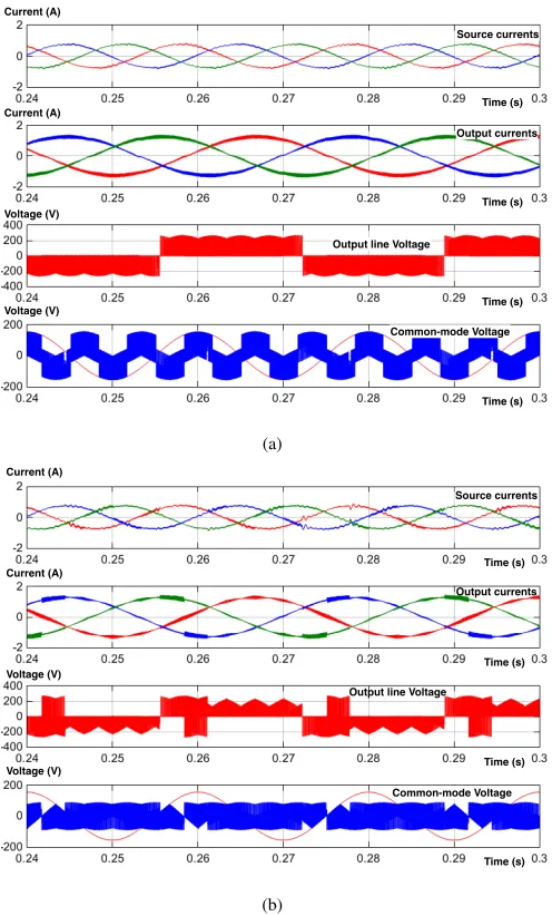
to verify the analysis. As shown in Fig. 8, both methods can maintain a set of sinusoidal and balanced input and output currents. The last subfigures in Fig. 10(a) and Fig. 10(b) shows the CMV waveforms when two SVM methods are applied, where the input phase voltage vsa is also given by red color for easy comparison. The peak value of CMV when the MC is modulated by the proposed method is reduced to 89.8V, in comparison with that of155.6V when the traditional SVM is used. Therefore, a 42.3% reduction on the peak value of CMV can be achieved. In addition, the RMS of the CMV decreases from156V for the traditional SVM to61.5V for the proposed SVM. With closer look at the waveforms, parts of the instantaneous CMV in every switching period are reduced to zero when the proposed method is employed, as can be seen in Fig. 9(b). This phenomenon is not seen in Fig. 9(a) where the traditional SVM is employed. The OSCs are utilized in the former but not in the latter, which explains why the RMS of the CMV is decreased.
For the low VTR applications, the waveforms with the modulation index m= 0.5 for both methods are quite similar to their counterparts when m= 0.9 is applied, as shown in Fig. 10. In comparison with the traditional SVM, the proposed method reduces the peak value of CMV by the same extent as it is with m= 0.9. The RMS of the CMV is decreased by 45.4%, from114.8V to62.6V. For the proposed method, the major difference between the situations when m = 0.9
andm= 0.5 are applied can be seen from the detailed CVM waveforms in Fig. 11, where the OSCs are not used in the latter case and thus zero CMV cannot be seen in each switching period.
The spectra of the CMVs are also shown in Fig. 12. As can be seen, The proposed method has lower fundamental value of CMVs and major harmonic frequencies than the traditional SVM for both m= 0.9 andm= 0.5.
To compare the performance of both methods for full range of VTR, Fig. 13 shows the THD contents of the input and output currents. The simulations were carried out with the modulation index m varied from 0.3 to 1. The proposed method has lower THD than the conventional SVM method in the output currents, but this situation is reversed in the input currents.
Voltage (V)
Time (s)
Voltage (V)
Time (s)
Time (s)
Time (s) Current (A)
Current (A)
Source currents
Output currents
Output line Voltage
Common-mode Voltage
(a)
Voltage (V)
Time (s)
Voltage (V)
Time (s)
Time (s)
Time (s) Current (A)
Current (A)
Source currents
Output currents
Output line Voltage
Common-mode Voltage
[image:8.612.315.559.57.455.2](b)
Fig. 8. Simulation waveforms for the MC with (a) the traditional SVM, (b) the proposed SVM employed. Modulation indexm= 0.9. From top to bottom: the source currents, the output currents, the output line-to-line voltagesvAB, the common-mode voltagesvcm.
B. Experimental results
Output line-to-line Voltage
Common-mode voltage (Blue) Voltage (V)
Time (s) Input phase voltage (Red)
Voltage (V)
(a)
Output line-to-line Voltage
Common-mode voltage (Blue) Voltage (V)
Time (s) Input phase voltage (Red)
Voltage (V)
[image:9.612.315.563.55.466.2](b)
Fig. 9. The enlarged output line-to-line voltage and CMV waveforms of the MC with (a) the traditional SVM, (b) the proposed SVM employed. Modulation indexm= 0.9.
by the DSP to calculate the duty cycle for each switch state while the directions of the output currents are used in the FPGA to complete the commutation.
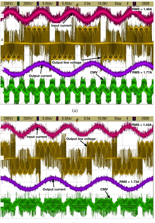
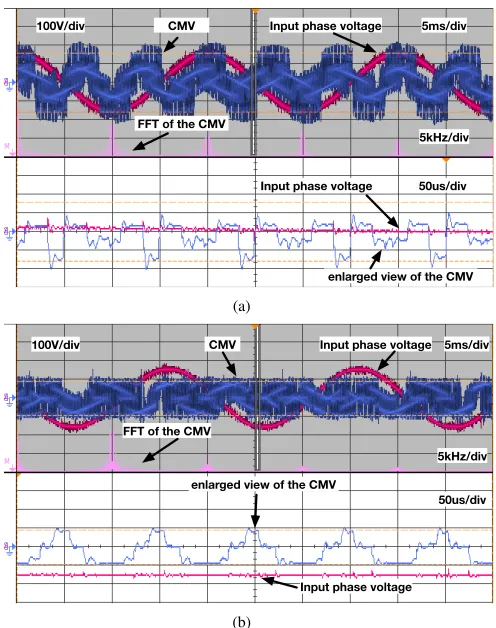
Fig. 15 shows the waveforms for the converters with m = 0.9. Both methods work well to maintain the source and output currents sinusoidal. The RMS of the CMV have been decreased from149V for the traditional SVM to62V for the proposed SVM. The peak value of CMV is also reduced from 156V in Fig. 16(a) to 90V in Fig. 16(b). Our proposal outperforms the traditional SVM in generating lower RMS and peak value of CMV. In consistent with the simulation results, the peak value of CMV can be reduced by about
42.3%. Note that ringing effect can be observed in the CMV waveforms due to the inductor at the loads. This effect extends the peak-to-peak value of the CMV. But even taking it into account, the proposed method has smaller CMV peak value than the traditional SVM. As can be seen from the enlarged waveforms of the CMV in Fig. 16, parts of the instantaneous CMV in every switching period are reduced to zero when the proposed method is employed, which can not be observed in the traditional SVM. In addition, the spectra of the CMV in this figure show that the proposed method has lower harmonics than the conventional SVM in the frequency band higher than the sampling frequency.
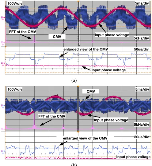
Similarly, Fig. 17 and Fig. 18 show the performance of the MC when the modulation indices for both methods are set to 0.5. Both methods are able to maintain the input and output currents sinusoidal in the low VTR applications, using the ZSCs rather than the OSCs. As shown in Fig. 18, the zero instantaneous CMV cannot be seen from the zoomed waveforms anymore. In comparison with the traditional SVM, the proposed method reduces the peak value of the CMV by a similar extent as in the situation when the MC is modulated atm= 0.9. Reductions on the RMS of the CMV, up to46.1%
from 150.7V to81.2V, can be measured. The ZSC with the
Voltage (V)
Time (s)
Voltage (V)
Time (s)
Time (s)
Time (s) Current (A)
Current (A)
Source currents
Output currents
Output line Voltage
Common-mode Voltage
(a)
Voltage (V)
Time (s)
Voltage (V)
Time (s)
Time (s)
Time (s) Current (A)
Current (A)
Source currents
Output currents
Output line Voltage
Common-mode Voltage
[image:9.612.53.299.57.275.2](b)
Fig. 10. Simulation waveforms for the MC with (a) the traditional SVM, (b) the proposed SVM employed. Modulation indexm= 0.5. From top to bottom: the source currents, the output currents, the output line-to-line voltagesvAB, the common-mode voltagesvcm.
intermediate input voltage not only has lower the peak value of CMV, but also makes the transition of the CMV lower. This accounts for the reduction on both the peak value and the RMS of the CMV observed in the proposed SVM. From the figures shown, the FFT analyses of CMV waveforms are also in well accordance with the simulation results.
Further, Fig. 19 is shown to validate that the proposed SVM method can can transit from low to high VTRs or reverse cases. The modulation indexm is set asm= 0.3 at first and then set as m = 0.9 through the host port interface (HPI). The transience is then captured by the oscilloscope. In this circumstance, the input voltage is set to 35V to avoid any possible disruption on the prototype system. As can be seen, during the transience, the modulation strategy maintains both the input and output currents sinusoidal. The transient state can switch smoothly without interruption.
Output line-to-line Voltage
Common-mode voltage (Blue) Voltage (V)
Time (s) Input phase voltage (Red)
Voltage (V)
(a)
Output line-to-line Voltage
Common-mode voltage (Blue) Voltage (V)
Time (s) Input phase voltage (Red)
Voltage (V)
(b)
Fig. 11. The enlarged output line-to-line voltage and CMV waveforms for the MC with (a) the traditional SVM, (b) the proposed SVM employed. Modulation indexm= 0.5.
and 4930timer counts respectively. With respect to the CPU clock rate at 225M Hz, the time consumption increases from
82.84µsto the87.64µs. The difference is acceptable given the sampling period is 100µs. Therefore, the proposed method needs only similar computation overhead to the traditional SVM.
VI. CONCLUSIONS
A novel SVD-based SVM technique to reduce the common-mode voltage (CMV) at the output side of a matrix converter has been proposed in this work. The reduction is achieved by including either the orientation switch configurations for the case of high voltage transfer ratio (VTR), or the zero switch configurations connecting to the input phase with the medium voltage for the case of low VTR, in the switching sequences. The orientation switch configurations are introduced in by substituting their equivalent switch configurations, without affecting the synthesis of the reference variables. Parts of CMV waveforms during the time intervals for the orientation switch configurations are decreased to zero. Therefore, not only the peak value but also the RMS of the CMV are reduced. The feasibility of the proposed SVM method is substantiated by the simulation as well as the experiment results.
REFERENCES
[1] P. Wheeler, J. Rodriguez, J. Clare, L. Empringham, and A. Weinstein, “Matrix converters: a technology review,”IEEE Trans. Industrial Elec-tronics, vol. 49, no. 2, pp. 276–288, 2002.
[2] L. Empringham, J. Kolar, J. Rodriguez, W. Patrick, and J. Clare, “Technological issues and industrial application of matrix converters: A review,”IEEE Trans. Industrial Electronics, vol. 60, no. 10, pp. 4260– 4271, 2013.
[3] J. Rodriguez, M. Rivera, J. Kolar, and P. Wheeler, “A review of control and modulation methods for matrix converters,”IEEE Trans. Industrial Electronics, vol. 59, no. 1, pp. 58–70, 2012.
[4] S. Chen, T. Lipo, and D. Fitzgerald, “Source of induction motor bearing currents caused by PWM inverters,”IEEE Trans. Energy Conversion, vol. 11, no. 1, pp. 25–32, 1996.
(a)
(b)
(c)
[image:10.612.318.562.56.492.2](d)
Fig. 12. The spectra of the CMV waveforms for the MC with (a) the traditional SVM andm= 0.9, (b) the proposed SVM andm= 0.9, (c) the traditional SVM andm= 0.5, and (d) the proposed SVM andm= 0.5 are employed. All magnitude values are calculated with respect to the base value of 100.
[5] U. Shami and H. Akagi, “Identification and discussion of the origin of a shaft end-to-end voltage in an inverter-driven motor,”IEEE Trans. Power Electronics, vol. 25, no. 6, pp. 1615–1625, 2010.
[6] N. Zhu, D. Xu, B. Wu, N. Zargari, M. Kazerani, and F. Liu, “Common-mode voltage reduction methods for current-source convert-ers in medium-voltage drives,”IEEE Trans. Power Electronics, vol. 28, no. 2, pp. 995–1006, 2013.
[7] J. M. Erdman, R. J. Kerkman, D. W. Schlegel, and G. L. Skibinski, “Effect of PWM inverters on AC motor bearing currents and shaft voltages,”IEEE Trans. Industry Applications, vol. 32, no. 2, pp. 250– 259, 1996.
[8] R. Baranwal, K. Basu, and N. Mohan, “Carrier-Based Implementation of SVPWM for Dual Two-Level VSI and Dual Matrix Converter With Zero Common-Mode Voltage,”IEEE Trans. Power Electronics, vol. 30, no. 3, pp. 1471–1487, 2015.
[image:10.612.54.299.57.275.2]0.00%$ 1.00%$ 2.00%$ 3.00%$ 4.00%$ 5.00%$ 6.00%$
0.3$ 0.4$ 0.5$ 0.6$ 0.7$ 0.8$ 0.9$ 1$
[image:11.612.316.564.54.410.2]CONV_Iin$ CONV_Iout$ PRO_Iin$ PRO_Iout$
Fig. 13. THD contents of the input and output currents for the proposed and the traditional SVM methods.
Matrix Converter
[image:11.612.59.289.58.174.2]Digital Controller (DSP + FPGA)
Fig. 14. A direct matrix converter prototype with its control platform.
[10] J. Riedemann, R. Pena, R. Cardenas, J. Clare, P. Wheeler, and M. Rivera, “Common mode voltage and zero sequence current reduction in an open-end load fed by a two output indirect matrix converter,” inProc. 15th European Conf. Power Electronics and Applications (EPE ’13), pp. 1–9, 2013.
[11] R. Gupta, K. Mohapatra, A. Somani, and N. Mohan, “Direct-matrix-converter-based drive for a three-phase open-end-winding AC machine with advanced features,”IEEE Trans. Industrial Electronics, vol. 57, no. 12, pp. 4032–4042, 2010.
[12] S. Tewari, R. K. Gupta, and N. Mohan, “Three-level indirect matrix con-verter based open-end winding AC machine drive,” inProc. 37th Annual Conf. IEEE Industrial Electronics Society (IECON ’11), pp. 1636–1641, 2011.
[13] S. Nath and N. Mohan, “A matrix converter fed sinusoidal input output three winding high frequency transformer with zero common mode voltage,” inProc. Int. Conf. Power Engineering, Energy and Electrical Drives (POWERENG), pp. 1–6, 2011.
[14] R. Gupta, K. Mohapatra, and N. Mohan, “Open-end winding AC drives with enhanced reactive power support to the grid while eliminating switching common-mode voltage,” inProc. 35th Annual Conf. IEEE Industrial Electronics (IECON ’09), pp. 700–707, 2009.
[15] M. Braun and A. Stahl, “Enhancing the control range of a matrix converter with common mode free output voltage,” inProc. 11th Int. Conf. Optimization of Electrical and Electronic Equipment (OPTIM ’08), pp. 189–195, 2008.
[16] K. Mohapatra and N. Mohan, “Open-end winding induction motor driven with matrix converter for common-mode elimination,” inProc. Int. Conf. Power Electronics, Drives and Energy Systems (PEDES ’06), pp. 1–6, 2006.
[17] F. Yue, P. W. Wheeler, and J. C. Clare, “Mitigation of common-mode voltage in matrix converter,” in Proc. The 3rd IET Int. Conf. Power Electronics, Machines and Drives, (PEMD ’06), pp. 296–300, 2006. [18] H.-H. Lee, H. Nguyen, and T.-W. Chun, “A study on rotor FOC
method using matrix converter fed induction motor with common-mode voltage reduction,” inProc. 7th Int. Conf. Power Electronics (ICPE ’07), pp. 159–163, 2007.
[19] T. Shi, Q. Huang, Y. Yan, and C. Xia, “Suppression of common mode voltage for matrix converter based on improved double line voltage
Input current
CMV Output current
Output line voltage
RMS = 1.46A
RMS = 1.77A
(a)
Input current
CMV Output current
Output line voltage
RMS = 1.42A
RMS = 1.73A
(b)
Fig. 15. Waveforms for the MC with (a) the traditional SVM, (b) the proposed SVM employed. Modulation indexm= 0.9. From top to bottom: the input currentia, the output line-to-line voltagesvAB, the output currentiA, the common-mode voltagesvcm.
synthesis strategy,”IET Power Electronics, vol. 7, no. 6, pp. 1384–1395, 2014.
[20] T. D. Nguyen and H.-H. Lee, “Modulation strategies to reduce common-mode voltage for indirect matrix converters,” IEEE Trans. Industrial Electronics, vol. 59, no. 1, pp. 129–140, 2012.
[21] T. Nguyen and H.-H. Lee, “A new SVM method for an indirect matrix converter with common-mode voltage reduction,”IEEE Trans. Industrial Informatics, vol. 10, no. 1, pp. 61–72, 2014.
[22] H.-N. Nguyen and H.-H. Lee, “A new SVM method to reduce common-mode voltage in direct matrix converter,” in Proc. 2014 Int. Power Electronics Conf. (IPEC-Hiroshima 2014-ECCE-ASIA), pp. 1013–1020, 2014-05.
[23] H.-N. Nguyen and H.-H. Lee, “A DSVM Method for Matrix Converters To Suppress Common-mode Voltage with Reduced Switching Losses,”
IEEE Trans. Power Electronics, vol. PP, no. 99, pp. 1–1, 2015. [24] H.-H. Lee and H. Nguyen, “An effective direct-SVM method for matrix
converters operating with low-voltage transfer ratio,”IEEE Trans. Power Electronics, vol. 28, no. 2, pp. 920 –929, 2013.
[25] H. Nguyen, H.-H. Lee, and T.-W. Chun, “An investigation on direct space vector modulation methods for matrix converter,” in Proc. 35th Annual Conf. IEEE Industrial Electronics (IECON ’09), pp. 4493–4498, 2009.
[26] H. J. Cha and P. N. Enjeti, “An approach to reduce common-mode voltage in matrix converter,”IEEE Trans. Industry Applications, vol. 39, no. 4, pp. 1151–1159, 2003.
[27] J.-K. Kang, T. Kume, H. Hara, and E. Yamamoto, “Common-mode voltage characteristics of matrix converter-driven AC machines,” in
[image:11.612.64.285.212.357.2]Input phase voltage 100V/div
FFT of the CMV
enlarged view of the CMV 5ms/div
50us/div 5kHz/div
Input phase voltage CMV
(a)
CMV Input phase voltage 100V/div
FFT of the CMV
enlarged view of the CMV
5ms/div
50us/div 5kHz/div
Input phase voltage
[image:12.612.52.300.52.366.2](b)
Fig. 16. Detailed CMV waveforms with (a) the traditional SVM, (b) the proposed SVM. Modulation indexm= 0.9. From top to bottom, the CMV waveforms, the FFT analyses of the CMV waveforms, and the enlarged view of the CMV waveforms.
[28] L. Hua, H. Bi, and Z. Xiaofeng, “A modulation strategy to reduce common-mode voltage for current-controlled matrix converters,” in
Proc. 32nd Annual Conf.IEEE Industrial Electronics (IECON ’06), pp. 2775–2780, 2006.
[29] F. Yue, P. Wheeler, and J. Clare, “Common-mode voltage in matrix converters,” inProc. 4th IET Conf. Power Electronics, Machines and Drives (PEMD ’08), pp. 500–504, 2008.
[30] C. Ortega, A. Arias, C. Caruana, and M. Apap, “Reducing the common mode voltage in a DTC-PMSM drive using matrix converters,” inProc. IEEE Int. Symp. Industrial Electronics (ISIE ’08), pp. 526–531, 2008. [31] L. Huber and D. Borojevic, “Space vector modulated three-phase to
three-phase matrix converter with input power factor correction,”IEEE Trans. Industry Applications, vol. 31, no. 6, pp. 1234–1246, 1995. [32] P. Nielsen, F. Blaabjerg, and J. Pedersen, “Space vector modulated
ma-trix converter with minimized number of switchings and a feedforward compensation of input voltage unbalance,” inProc. Int. Conf. Power Electronics, Drives and Energy Systems for Industrial Growth, vol. 2, pp. 833–839, 1996.
[33] O. Simon and M. Braun, “Theory of vector modulation for matrix converters,” inProc. EPE ’01, pp. 1–7, 2001.
[34] H. Hojabri, H. Mokhtari, and C. Liuchen, “A generalized technique of modeling, analysis, and control of a matrix converter using SVD,”IEEE Trans. Industrial Electronics, vol. 58, no. 3, pp. 949–959, 2011. [35] P. Kiatsookkanatorn and S. Sangwongwanich, “A unified PWM method
for matrix converters and its carrier-based realization using dipolar modulation technique,” IEEE Trans. Industrial Electronics, vol. 59, no. 1, pp. 80–92, 2012.
[36] L. Zarri, M. Mengoni, A. Tani, and J. Ojo, “Range of the linear mod-ulation in matrix converters,”IEEE Trans. Power Electronics, vol. 29, no. 6, pp. 3166–3178, 2013.
[37] H. Hojabri, H. Mokhtari, and L. Chang, “Reactive power control of permanent-magnet synchronous wind generator with matrix converter,”
IEEE Trans. Power Delivery, vol. 28, no. 2, pp. 575–584, 2013. [38] D. Casadei, G. Serra, A. Tani, and L. Zarri, “Matrix converter
modula-tion strategies: a new general approach based on space-vector
represen-Input current
CMV Output current
Output line voltage
RMS = 627mA
RMS = 720mA
(a)
Input current
CMV Output current
Output line voltage
RMS = 573.5 mA
RMS = 680 mA
[image:12.612.315.562.52.416.2](b)
Fig. 17. Waveforms for the MC with (a) the traditional SVM, (b) the proposed SVM employed. Modulation indexm= 0.5. From top to bottom: the input currentia, the output line-to-line voltagesvAB, the output currentiA, the common-mode voltagesvcm.
tation of the switch state,”IEEE Trans. Industrial Electronics, vol. 49, no. 2, pp. 370–381, 2002.
[39] Y. Tadano, S. Urushibata, M. Nomura, Y. Sato, and M. Ishida, “Direct space vector PWM strategies for three-phase to three-phase matrix converter,” inProc. Power Conversion Conference, PCC ’07, pp. 1064– 1071, 2007.
[40] Y. Tadano, S. Hamada, S. Urushibata, M. Nomura, Y. Sato, and M. Ishida, “Direct space vector PWM strategy for matrix converters with reduced number of switching transitions,”Electrical Engineering in Japan, vol. 172, no. 3, p. 5263, 2010.
[41] J. Espina, C. Ortega, L. de Lillo, L. Empringham, J. Balcells, and A. Arias, “Reduction of output common mode voltage using a novel SVM implementation in matrix converters for improved motor lifetime,”
IEEE Trans. Industrial Electronics, vol. 61, no. 11, pp. 5903 – 5911, 2014.
[42] H.-N. Nguyen and H.-H. Lee, “An Enhanced SVM Method to Drive Matrix Converters for Zero Common-Mode Voltage,” IEEE Trans. Power Electronics, vol. 30, no. 4, pp. 1788–1792, 2015.
[43] C. Garcia, M. Rivera, M. Lopez, J. Rodriguez, P. Wheeler, R. Pena, J. Espinoza, and J. Riedemann, “Predictive current control of a four-leg indirect matrix converter with imposed source currents and common-mode voltage reduction,” inProc. IEEE Energy Conversion Congress and Exposition (ECCE ’13), pp. 5306–5311, 2013.
[44] M. Rivera, J. Rodriguez, J. Espinoza, and B. Wu, “Reduction of common-mode voltage in an indirect matrix converter with imposed sinusoidal input/output waveforms,” inProc. 38th Annual Conf. IEEE Industrial Electronics Society (IECON ’12), pp. 6105–6110, 2012. [45] R. Vargas, U. Ammann, J. Rodriguez, and J. Pontt, “Predictive strategy
CMV Input phase voltage 100V/div
FFT of the CMV
enlarged view of the CMV
5ms/div
50us/div 5kHz/div
Input phase voltage
(a)
CMV
Input phase voltage 100V/div
FFT of the CMV
enlarged view of the CMV
5ms/div
50us/div 5kHz/div
Input phase voltage
[image:13.612.52.300.55.325.2](b)
Fig. 18. Detailed CMV waveforms for (a) the traditional SVM and (b) the proposed SVM. Modulation indexm= 0.5. From top to bottom, the CMV waveforms, the FFT analyses of the CMV waveforms, and the enlarged view of the CMV waveforms.
Input phase voltage
Output current Input current Output line voltage
Fig. 19. The transient process of the proposed SVM method from high to low VTR regions. From top to bottom: the input phase voltageva, the input currentia, the output line-to-line voltagesvAB, the output currentiA.
IEEE Trans. Industrial Electronics, vol. 55, no. 12, pp. 4372–4380, 2008. [46] R. Vargas, U. Ammann, J. Rodriguez, and J. Pontt, “Predictive strategy to reduce common-mode voltages on power converters,” inProc. IEEE Power Electronics Specialists Conf. (PESC ’08), pp. 3401–3406, 2008. [47] Q. Guan, P. Yang, Q. Guan, and X. Wang, “SVD-based indirect space vector modulation with feedforward compensation for matrix convert-ers,” inProc. 39th Annual Conference of the IEEE Industrial Electronics Society (IECON ’13), pp. 4955–4960, 2013.
[48] A. Alesina and M. Venturini, “Analysis and design of optimum-amplitude nine-switch direct AC-AC converters,” IEEE Trans. Power Electronics, vol. 4, no. 1, pp. 101–112, 1989.
[49] J. W. Kolar, F. Schafmeister, S. D. Round, and H. Ertl, “Novel three-phase AC-AC sparse matrix converters,”IEEE Trans. Power Electronics, vol. 22, no. 5, pp. 1649–1661, 2007.
[50] A. Alesina and M. Venturini, “Solid-state power conversion: A fourier analysis approach to generalized transformer synthesis,” IEEE Trans. Circuits and Systems, vol. 28, no. 4, pp. 319–330, 1981.
[51] E. Un and A. Hava, “Performance characteristics of the reduced common mode voltage near state PWM method,” in Proc. 2007 European Conference on Power Electronics and Applications, pp. 1–10, 2007. [52] E. Un and A. Hava, “A near-state PWM method with reduced switching
losses and reduced common-mode voltage for three-phase voltage source inverters,”IEEE Trans. Industry Applications, vol. 45, no. 2, pp. 782– 793, 2009.
[53] A. Hava and E. Un, “A high-performance PWM algorithm for common-mode voltage reduction in three-phase voltage source inverters,”IEEE Trans. Power Electronics, vol. 26, no. 7, pp. 1998–2008, 2011. [54] Q. Guan, P. Yang, X. Wang, and X. Zhang, “Stability analysis of matrix
converter with constant power loads and LC input filter,” inProc. 7th IEEE Int. Power Electronics and Motion Control Conf. (IPEMC’12), vol. 2, pp. 900 –904, 2012.
[55] J. Dasika and M. Saeedifard, “An Online Modulation Strategy to Control the Matrix Converter Under Unbalanced Input Conditions,”IEEE Trans. Power Electronics, vol. 30, no. 8, pp. 4423–4436, 2015.
[56] P. Wheeler, J. Clare, and L. Empringham, “Enhancement of matrix converter output waveform quality using minimized commutation times,”
IEEE Trans. Industrial Electronics, vol. 51, no. 1, pp. 240–244, 2004.
Quanxue Guan (S’11) received the B.Eng. degree in automation engineering from the South China University of Technology (SCUT), Guangzhou, China in 2007. He was a project engineer in HILTI (China) Ltd. after graduate. He have been working toward his Ph.D. degree in SCUT since 2009. He be-came a visiting researcher at the Power Electronics, Machines and Control Group in the University of Nottingham in 2014. His current research interests are in modulation and control of matrix converters.
Patrick W. Wheeler (M’00-SM’13) received his BEng [Hons] degree in 1990 from the University of Bristol, UK. He received his PhD degree in Elec-trical Engineering for his work on Matrix Converters from the University of Bristol, UK in 1994. In 1993 he moved to the University of Nottingham and worked as a research assistant in the Department of Electrical and Electronic Engineering. In 1996 he became a Lecturer in the Power Electronics, Machines and Control Group at the University of Nottingham, UK. Since January 2008 he has been a Full Professor in the same research group. He is currently Head of the Department of Electrical and Electronic Engineering at the University of Nottingham. He is an IEEE PELs Member at Large and an IEEE PELs Distinguished Lecturer. He has published over 400 academic publications in leading international conferences and journals.
Quansheng Guan(S’09-M’11) received the B. Eng. degree in electronic engineering from Nanjing Uni-versity of Post and Telecommunications, China, in 2006 and the Ph.D. degree from South China Univer-sity of Technology, China, in 2011. He is currently a faculty member with the School of Electronic and Information Engineering, South China University of Technology. His research areas include topology control, routing and cooperative communications for mobile ad hoc networks, and cognitive networks.
[image:13.612.49.302.383.557.2]