Department of Mechanical System Science, Graduate School of Science and Engineering, Yamagata University, Yonezawa, Yamagata 992-8510, Japan
Hybrid functional materials, constituting both inorganic and organic components, are considered potential platforms for applications in extremely diverse fields such as optics, micro-electronics, transportation, health, energy, energy storage, diagnosis, housing, environment and the highly relevant area is Internet of Things (IoT). Material properties of hybrid materials can be tuned by modification of the composition on the molecular scale to produce smart materials. Cross-cutting approaches, to synergistically couple molecular engineering and processing allows to tailor complex hybrid systems of various shapes with perfect control over size, composition, functionality, and morphology. The detailed description and discussion of variety of hybrid functional organic-inorganic materials and their contribution in the designing of specific modern technologies is the prime focus of this review. © The Author(s) 2018. Published by ECS. This is an open access article distributed under the terms of the Creative Commons Attribution 4.0 License (CC BY,http://creativecommons.org/licenses/by/4.0/), which permits unrestricted reuse of the work in any medium, provided the original work is properly cited. [DOI:10.1149/2.0191808jes]
Manuscript submitted January 31, 2018; revised manuscript received April 20, 2018. Published May 4, 2018.This paper is part of the JES Focus Issue on Ubiquitous Sensors and Systems for IoT.
There is an enormous demand for hybrid materials to provide tech-nological breakthroughs with the most sought after being the enabling of the IoT. Interest in the field of IoT will witness exponential growth over the next decade as markets realize the true potential of real-time data acquisition for various entertainment, knowledge dissemina-tion, defense, environmental, and healthcare applications. Many of the well-established materials, such as metals,1ceramics,2–4or plastics5,6
cannot fulfill all technological desires for the various new applica-tions. In addition to the early interest in structural hybrid materials based on carbon-silicon networks, many recent efforts have centered on the design of functional hybrid materials which harness the chemi-cal activity of their components. This approach has been successfully used in recent years in the design of hybrid polymers7with special
em-phasis on structural hybrid materials based on mixed silicon-carbon networks prepared by sol-gel methods8–12which can also entrap
ad-ditional active species.13In this field the stakes are high and scientists
aim at producing structural materials with properties between those of inorganic glasses and organic polymers.8 But the expectations
go beyond mechanical strength and thermal and chemical stability. These new materials are also sought for improved optical,14–17and
electrical18,19properties, luminescence,12,20–25ionic conductivity,26–28
and selectivity,29–32as well as chemical33–35 or biochemical36–38
ac-tivity. Chemical activity is of core importance in functional materials. Sensors, selective membranes, all sorts of electrochemical devices, from actuators to batteries or supercapacitors, supported catalysts or photoelectrochemical energy conversion cells are some important de-vices based on hybrid functional materials.
Hybridization is a multifaceted strategy. In some cases, conduct-ing organic polymers act just as a solid polymeric support for active species, whereas in other hybrid systems the activity of organic and inorganic species combines to reinforce or modify each other. But in every case the work on these hybrid materials involves the underly-ing use and sometimes even the explicit search for synergy. Hybrid
∗Electrochemical Society Member.
zE-mail:[email protected];[email protected]
organic-inorganic materials in general represent the natural interface between two worlds of chemistry each with very significant contri-butions to the field of materials science, and each with characteristic properties that result in distinct advantages and limitations. Research in the topic of hybrid materials has challenges and opportunities. The main challenge is managing to synthesize hybrid materials that keep or enhance the best properties of each of the components while reduc-ing their particular limitations. Undertakreduc-ing this challenge provides an opportunity for developing new materials with synergic behavior leading to improved performance or to new useful properties. Indeed, hybrid materials frequently involve a combination of components that have been thoroughly studied in their respective fields but provide an additional dimension to their properties in becoming part of the hybrid compound.
Hybrid materials can demonstrate better properties compared with their individual counterparts, where in inorganic material can play several roles: enhancing the mechanical and thermal stability, modu-lating the refractive index, providing an accessible and interconnected porous network for sensing or catalysts, or contributing specific mag-netic, electronic, redox, electrochemical or chemical properties. Or-ganic components greatly extend the range of matrices available to synthetic chemists. Organic materials can offer opportunities to mod-ify mechanical properties enabling the production of films and fibers, to obtain by simple casting various geometric structures for integrated optics, to control the porosity and connectivity of networks, and to adjust the balance hydrophilic/hydrophobic character. Organic com-ponents can also contribute a specific physical or chemical property including electrical or optical characteristics, electrochemical behav-ior, chemical or biochemical reactivity, etc.
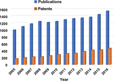
In the last decades hybrid materials were developed on a large scale with a lot of realized economic applications. The increase in the publications and patent applications from the 2005 until the year 2016 is tremendous as shown in Fig. 1. Due to the possibility of designing properties through the hybridization of the organic and in-organic components, multifunctional materials39,40 can be created.
B3138 Journal of The Electrochemical Society,165(8) B3137-B3156 (2018)
Figure 1. Number of papers published in last decade on hybrid materials.
(Source: SciFinder Scholar:https://scifinder-n.cas.org).
treatment, e.g., scratch resistant coatings.41–43Based on the
molecu-lar or nanoscale dimensions of the building blocks, light scattering in homogeneous material can be avoided and optically transparent nanocomposite materials suitable for optical applications can be pro-duced.44–47In some cases phase separation of organic and inorganic components is used for the formation of porous materials.48,49Smart
materials can be fabricated by modification of the composition on the molecular scale. For example, electroactive materials,50,51
elec-trochromic materials,52–54sensors,55–57membranes,58,59and biohybrid
materials.60–62 This review will center on organic-inorganic hybrid
materials and their utilization as optical and electronic functional ma-terials for development of new technologies. Mostly, we will focus on organic-inoragnic hybrid materials containing polymers as one of the component, which has brodned the scope of hybrid materials for diverse areas of applications.63–71
Categorization of Functional Hybrid Materials
Functional hybrid materials are not just a physical mixture. They are nanocomposites at the molecular scale, having at a minimum one component, either the organic or the inorganic constituting part, with a characteristic length on the nanometer size (a few Å to several tens of nanometers).72The sum of the all properties of the hybrid
materi-als are not the outcome of properties individual contributions of their components, but also from the strong synergy created by a hybrid interface.73,74The nature of the inorganic/organic interface, including
the types of interactions present, the surface energy, and the exis-tence of labile bonds plays a strong role in controlling of a number of properties (electrical, optical, mechanical, separation capacity, catal-ysis, sensing capability, and chemical and thermal stability). Owing to their large importance, various functional hybrid materials can be categorized into two main families depending on the nature of the in-terface combining the organic components and inorganic materials.72
Class I deals with hybrid systems where the organic and inorganic parts interact by weak bonds including Van der Waals, electrostatic or hydrogen bonds. Class II indicates hybrid materials in which these components are linked by covalent or ionic-covalent chemical bonds. Indeed, various hybrid materials consist of both types of interfaces, strong and weak, but due to the significance of the presence of strong chemical bonds on the final hybrid material properties, these types of hybrid are grouped into class II. The compounds of hybrid class I present a number of interesting features such as ease of synthesis of the material, the avoidance of heterofunctional metal-organic pre-cursors, and, when desired, the facile removal of the organic phase to easily create functional architectures by self-assembly. However, currently we are witnessing the increasing development of hybrid ma-terials of class II. The existence of covalent chemical bonds between
organic and mineral components presents a number of advantages: i) the potential to synthesis entirely new materials from functionalized alkoxides, ii) minimization of phase separation, and iii) better defini-tion of the organic-inorganic interface. Such defined control can lead to a better understanding of the material and the relationship between microstructure and properties, an easier adjustment of the hydrophilic-hydrophobic balance, etc. Effective grafting of organic functionality to the inorganic network avoids a drawback of the hybrid compounds of Class I. That is the potential departure of organic components while the material is in use, e.g. in applications like sensors or catalysts.
Synthetic methodologies for hybrid materials.—Irrespective of type of hybrid interface there are numerous synthetic strategies and processes present for the fabrication and formation of hybrid materials.74–77 The fundamental synthetic strategies are illustrated
schematically in Fig. 2. The reaction route (path A, Fig.2) repre-sents sol-gel as well as hydro- and solvothermal synthesis, where molecular precursors such as alkoxides, metal salts in the presence of complexing polyfunctional precursors, and organofunctional pre-cursors are used. In this case organic functionality is a non-labile terminal or bridging organic, R. Sol–gel (path A1, Fig.2) involv-ing hydrolysis and condensation reactions from alcoxyorganosilanes or alcoxyorganostannanes (RSi(OR)3, R-Sn(OR)3 where R is an organic functionality) of alkoxides or metal halides (M(OR)n,MXn
with M=Ti, Zr, Nb, Al etc.) and mixtures thereof. However, these materials are generally amorphous with polydispersed size distribu-tions, and this complexity makes it difficult to study their structure-properties relationships. Path B (Fig.2) illustrates strategies based on the assembly of preformed monodispersed nano-objects.74,77–79These
nano-objects can be clusters or nanoparticles (metal oxides, metals and alloys, chalcogenides), nanoparticle composite type core/shell, or nano-sheets of lamellar compounds (clays, double hydroxides, phos-phates, oxides and lamellar chalcogenides). These nano-objects, in their various compositions, must be stable under the chemical condi-tions imposed during assembly. Therefore, they are very often pre-or post-hybridized by attaching organic components to their surface in order to provide greater stability and transferability in the assembly en-vironment (aqueous or non-aqueous solvents, within polymers, etc.). These nano objects can be surface functionalized with polymerizable ligands, spacers, organic molecules or telechelic polymers, functional dendrimers, biomolecules, etc. The use of preformed hybrid objects opens the way for “legochemistry” which allows the building of cus-tom materials or hybrid assemblies. This modular approach from nano objects presents a number of advantages. The step-by-step develop-ment of the material allows better control of its structure on the semi-local scale. Prefabricated nano-objects often show reduced reactivity compared to that of molecular precursors; the inorganic component is relatively monodispersed on the nanometer scale allowing the devel-opment of more well-defined structures that facilitate characterization and control over the quality of the final material.
Path C exploits the self-assembly properties of amphiphilic molecules and polymers to generate supramolecular templates to control the texture and morphology of the growing solid or gel phase.74,75,79,80 These inorganic or hybrids phases can be generated
from precursors previously described in paths A and B (molecular clusters, nanoparticles, etc.). Two approaches are currently being ex-plored: i) using preorganized organic, biological, or inorganic tem-plates, akin to structural molds for casting the material and ii) syner-gistic assembly where the precursors and texturing agents (templates) are co-assembled in situ into organized architectures.81,82Path C is
Figure 2. Synthetic Methadologies of hybrid functional materials (Reproduced with permission from Ref.79, copyright 2010, Wiley).
organization and porosity accessible to a secondary functionalization via post grafting.81
Path D is an integrative approach in which the chemical arsenal described above can be combined with templates of variable size (organo-gelifiers, bacteria, latex beads, submicron colloidal minerals) and the physical chemistry of soft matter. This is described mainly in the context of production processes (nano-molding and multiple replications, reactive extrusion, electrospinning). It also may involve morpho-synthesis, which involves chemical transformations in con-fined geometries: micro-emulsions, micelles, vesicles, etc., phase separation kinetically controlled by the gelification of the network (spinodal), the use of breath figures, or Rayleigh-Besnard instabil-ities, dissipatives structures, etc, as templating modes and textura-tion of materials induced by external stimuli (mechanical and opti-cal, electric or magnetic fields, etc.) generated during their formation process.75,79,83,84 These strategies in a single stage can generate
hy-brid materials with hierarchical structure. This structural hierarchy is one essential characteristic of biological materials, where topological and structural organization is present at all scales, from the nano or supramolecular, to the micro and often millimeter scale. These hier-archical structures observed in vivo present not only great complex-ity but also a high selectivcomplex-ity to external stimuli. Natural materials can serve as models to inspire and develop new concepts and new “biomimetic strategies” in materials engineering. Learning the skills of some living systems and transcribing the rules and methodology of their construction should enable us to develop new materials, with superior performance characteristics.79,85,86
Hybrid nanocomposite materials, synthesized from colloidal nanometer-sized particles of metals or metallic compounds dispersed in polymers has attracted great attention.87In these materials,
inor-ganic nanoparticles (NPs) are not the host for the intercalation of organic polymers, but at the same time they are too large to be con-sidered guest species conforming to the structure of the polymers. These materials could therefore be considered as true composite ma-terials where each component still retains its own structure but with an increased interfacial interaction derived from the small particle size. Within this category a first group of materials is formed by nanosized metal particles dispersed in polymers.88–92Most frequently the metals
used are precious metals, Pd and Pt, and the hybrids are designed for catalytic purposes, such as proton and oxygen reduction,88,93,94
hydro-gen oxidation88as well as hydrogenation reactions.89A second group
of materials is constituted by those in which the nanodispersed phase is an oxide. Several hybrid materials based on colloidal particles of transition metal oxides (g-Fe2O3,95,96MnO2,97,98CuO,99TiO2,100–102 and WO3103,104) as well as tin oxide105and silica105,106have been re-ported. In addition to the more extensively studied work on oxides, recent reports have extended this family of hybrid composites to other colloidal semiconducting particles such as CdS,107,108CdSe,106–108and
copper or silver halides.107
Nanoparticles (NPs), in the 1–100 nm sizes tend to bridge the gap between small molecules and bulk materials.109 As a class of
B3140 Journal of The Electrochemical Society,165(8) B3137-B3156 (2018)
Figure 3. Fabrication of amphiphilic Au(PB-PEG)nnanoparticles. (Reproduced with permission from Ref.117, copyright 2006, American Chemical Society).
the past decade due to their unique electronic, optical and catalytic properties.110,111These properties are neither those of bulk metal nor
those of molecular compounds as has been widely demonstrated in both experimental and theoretical investigations, but they strongly de-pend on the particle size, shape and interparticle distance as well as the nature of the protecting organic shell.112The chemical stability of
NPs is crucial to avoid degradation processes such as partial oxidation or undesired sintering of particles. The lack of sufficient stability of many NPs has impeded the development of real world applications of these nanomaterials.
The use of polymeric stabilizers for metal NPs has inspired the studies of various synthetic routes to link polymers to metal particles and the investigations on properties as well as potential applications of the hybrid materials. The advantages of using polymers as stabilizers are not only for the enhancement of long-term stability, adjustment of the solubility and amphiphilicity of NPs. They also include the functionalization of NPs with polymers to achieve higher and tun-able surface-density of shell/brush, to tailor properties of NPs, as well as to promote compatibility and processibility. For example, to assemble AuNP films with ordered structures, Genson et al.113 and
Zubarev et al.114 prepared AuNPs functionalized with amphiphilic
polybutadiene-poly(ethylene glycol) (PB-PEG) V-shaped arms by es-terification of PB-PEG chains to mercaptophenol-stabilized AuNPs (Fig.3). Approximately 65 V-shaped molecules were tethered to a pre-formed AuNP, resulting in a high grafting density of 0.2 nm2per V-shaped molecule. This value reaches the limits of the dense pack-ing of phenylbenzoate groups in the upright orientation. These am-phiphilic AuNPs formed stable Langmuir monolayers at the air/water and the air/solid interfaces. At these interfaces, the binary poly-mer arms vertically segregated into a dense polypoly-mer corona. These corona-surrounded the AuNPs, preventing their large-scale agglom-eration keeping individual nanoparticles well-separated from each other and forming flattened, pancake nanostructures. Composite ma-terials with ordered structures consisting of conducting polymers and metal nanoparticles are of great interest and promising for further applications in micro- and optoelectronics. Intelmann et al.115
pre-pared AuNPs on ultrathin films of polythiophene and polythiophene derivatives. The ultrathin films of polythiophene derivatives bearing hydroxyl groups were esterified with thioctic acid that contained a dithiolane moiety. The dithiolane moiety was utilized to immobilize AuNPs from a monodisperse gold sol synthesized by citrate reduc-tion. The immobilized AuNPs were not removed by Scotch tape tests, indicative of the successful adhesion of AuNPs on the films of poly-thiophene derivatives through a covalent bond formed between the dithiolane moiety and gold. Cho and Park116 reported the
sponta-neous deposition of Au and Ag NPs on sulfur containing conducting
polymer surfaces of poly(3-methylthiophene) (P3MeT) and poly(3,4-ethylenedioxythiophene) (PEDOT) by simply dipping the polymer films into colloid solutions containing these particles. The current– voltage curves indicated that the contacts between the particles and the polymer surfaces were ohmic, indicating potential applications in electrocatalysis for fuel cells as well as for electronic devices. Polymer-protected AuNPs were also prepared by encapsulating pre-formed colloidal AuNPs with water-soluble conductive poly(aniline-2-carboxylic acid) by Englebienne and Hoonacker117The composite
nanoparticles displayed significant enhancements in photonic perfor-mance, and offers new opportunities for biosensing applications.
Recently, our group has reported a facile networked alignment of AgNPs, attained and stabilized by employing a graft copolymer bear-ing C=S moieties (Fig.4). AgNPs in the complex were in uniform and nanosized. The cavity of the network of Ag complex manifested the translucency. The vertical conductivity under compression sug-gests potential applications for printable electronic devices such as touch screens. The high conductivity under strong compression is as-cribable to the reduced insulation by the compression of the softer polymer chains.
Mir et al.18has reported a facile one-pot approach for preparing
hierarchical nanowire-networks of hollow polymer@Pd nanospheres. The nanospheres were hierarchically assembled into the nanowire-network upon drying. The Pd nanowire-nanowire-network served as an active catalyst for Mizoroki–Heck and Suzuki–Miyaura coupling reactions with a trace amout of 500μmol % Pd was sufficient for quantita-tive reactions, due to the presence of highly acquantita-tive sites originating from high-index facets, kinks, and coalesced structures (Fig.5). The polymer@Pd nanosphere also served as a printable conductive ink for a translucent grid pattern with excellent horizontal conductivity (7.5×10⁵S m−1).
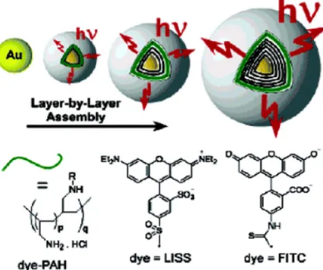
Metal nanostructures may have useful effects on the photolumi-nescence of nearby emitters. It has been found that chromophores sit-uated in the vicinity of isolated colloidal metal particles in suspension usually experience quenching of their fluorescence,118,119 Schneider
and Decher119 fabricated metal core–polymer shell capsules by use
of layer-by-layer (LBL) deposition of oppositely charged trolytes onto 13-nm-diameter AuNPs, where nonfluorescent polyelec-trolytes are spacer layers and fluorescent organic dyes are situated in the outer polymer layer (Fig.6).
Technology Driven Exploration of Hybrid Materials
Figure 4. Graft copolymer, polyTU-g-PtBMA-AgNP complex, (reproduced with permission from Ref.19a, copyright 2017, Springer).
in which the inorganic material (nanocrystals, colloids, polyoxomet-alates) is embedded in a polymeric matrix,120 and the other where
the organic polymer is confined into an inorganic template.121In the
first case, inorganic-in-organic composites, the good processability
Figure 5. SEM (a, b), TEM (c), HRTEM (d–f), and selected area electron
diffraction (SAED) pattern (inset in d) images of the Pd nanowire-network. (Reproduced with permission from Ref.18, Wiley).
and low density of the polymer component, in combination with the high mechanical durability and well-defined optoelectronic proper-ties of the inorganic component, are harnessed. This allows the com-binations of the advantages of the rapidly developing field in opto-electronic technology122with attractive properties of semiconductor
nanocrystals (NCs). Optical properties of this class of lumophores are determined by the quantum confinement effect, so that their emission color and the electron affinity can be finely controlled, not only by the material choice, but also by size within a single synthetic route.123,124
[image:5.585.39.282.447.717.2]Proper surface passivation leads to improved chemical stability and
Figure 6. Layer-by-layer assembly for the construction of core-shell
[image:5.585.310.542.521.715.2]B3142 Journal of The Electrochemical Society,165(8) B3137-B3156 (2018)
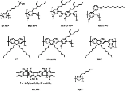
Figure 7. Chemical structures of the polymers used in blend systems for hybrid devices. Chemical structures are MEH-PPV, MEH-CN-PPV, P3HT, PF, F8BT,
CN-PPP, PF-co-PPV, yellow-PPV and MeLPPP.
high photoluminescence (PL) quantum yields of>50% for so-called core-shell NCs like CdSe/ZnS125 or CdSe/CdS,126 where the large
bandgap semiconductors (ZnS or CdS) epitaxially overgrow the core material (CdSe) and the band edges of the core material lie inside the bandgap of the outer material. Variable surface chemistry of NCs allows for the ease of their processability from different solvents and for their incorporation into different organic matrices. The basic idea behind NC based organic light-emitting diodes (OLEDs) is to achieve full color tuneability in a single host material. Organic semiconduc-tors such as conjugated polymers represent large polymer chains that are soft and flexible. On the other hand, semiconductor NCs as in-organic species are robust. Inin-organic semiconductors are well known to change their emission color over a very wide spectral range, while in organic semiconductors this effect is less pronounced and often goes in hand with changed electrical properties. Although organic molecules span the entire visible spectrum in terms of emission wave-length, a change of material required to tune the color of emission can result in a dramatic modification of the charge transport properties and thus of the device characteristics. A key goal of research into hy-brid NC-based OLEDs is therefore a separate optimization of charge transport and emission properties, which can be achieved in certain hybrid devices.127Whereas organic semiconductors are typically hole
transporting materials, NC solids generally display strongly n-type behavior,128 i.e. in most cases preferentially conduct electrons
mak-ing the two classes of materials a natural choice of partners. Therefore, combination of both components within nanocomposites enhances the range of potential optoelectronic applications.
Since the discovery of electroluminescence from conjugated poly-mers by Burroughes, Friend, Holmes and coworkers,129there has been
considerable industrial and academic interest in semiconducting poly-mers as the active material for electrolumnicence (EL) applications. There is a passionate pursuit of the design and development of ma-terials that meet application criteria such as desired emission colors with high emission intensity and efficiency, and good environmental
stability. In particular, the control of the emission color of charge-accepting and transporting properties (important for optimizing de-vice efficiency), and of electrical and optical stability (vital factors in determining device lifetimes) must be addressed. In light absorbing applications there is a stronger focus to tune the materials which have broad spectral response to the absorbed light and applying the con-ductive polymers, which have capacity of charge transport within the phase separated polymer domains on a mesoscopic level (nm-mm). Some of the most common methods to address the above-mentioned issues will be briefly discussed in the following sections.
The charge transport characteristics of only NCs is low130 and it
is difficult to obtain an electrical contact to single NCs because of their small size. Taking these aspects together, these particularities of NCs make them attractive materials for fabrication of hybrid semicon-ductor NC/organic devices as described below. The organic/inorganic compatibility depends on the versatile chemistry of the host polymer. Hence, the polymers are designed to attain both the optoelectronic properties desired for the specific application in mind, and chemical compatibility providing organic/inorganic homogeneous mixtures. In analogy to the already very successful donor/acceptor approach for phosphorescent systems,131wide bandgap semiconducting polymers
are used as donor hosts for semiconductor NCs.132In such blend
sys-tems, efficient energy transfer from host (polymer) to guest (NCs) takes place when the donor and acceptor moieties are in close spa-tial proximity and have a sufficient spectral overlap.132–135 Energy
and charge transfer from the polymer to the NCs requires an en-ergy band offset at the organic/inorganic interface. To date, conju-gated polymer hosts used in hybrid device technology include mainly the commercially available p-type wide bandgap polymers. MEH-PPV is the most common polymer used as host in hybrid light-absorbing or -emitting devices.136–140Some authors reported
yellow-PPV,140 CN-PPV141,142 or methylsubstituted ladder-type
poly(para-phenylene) (MeLPPP)143as hosts (Fig.7). Polyfluorene (PF) (n-type
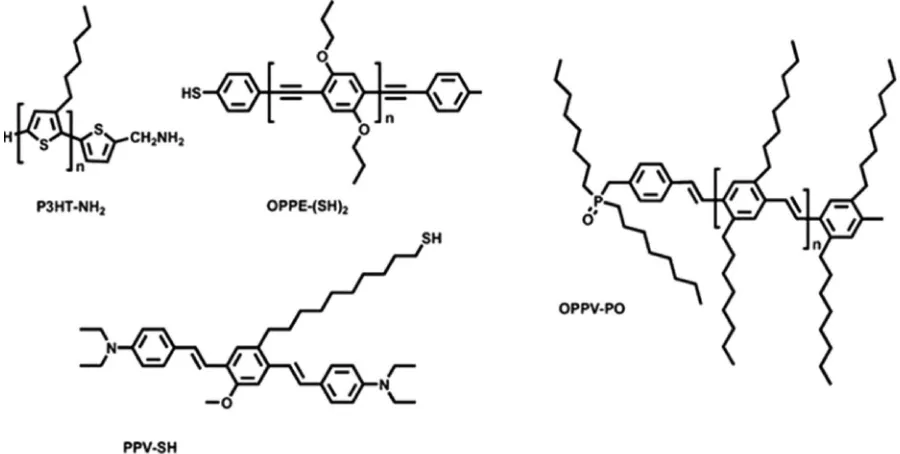
Figure 8. Chemical structures of end-group (end groups are connected to NCs) functionalized oligomers: P3HT,157bPPV-SH157cand OPPE (SH2)158as well as OPPV-PO.152
9,9-dialkylfluorenebenzothiadiazole (FxBT;x=6 or 8)144,145were also
recently used as polymer matrices in hybrid LEDs (Fig.6). Hybrid solar cells comprise mainly MEH-PPV137,139,146,147or p-type
semicon-ducting polymers of the polythiophene family such as P3HT146–148or
poly(3-octyl-thiophene) (P3OT).149A recent example of a red PF is
also available.150
Mixing NCs into commercially available cationic PF-based poly-electrolytes (Fig.8) resulted in improved NC stability, and reduced polymer interchain interactions.145 These effects are both desirable
in hybrid LEDs as they enhance the device stability and device effi-ciency by reducing non-radiative losses. A competitive approach to suppress polymer host interchain interaction is the introduction of linear152,153and side-functional,154or dendritic capping ligands.155–157
Mixing of NCs with polymers was also shown to result in enhanced energy transfer from the polymer to the NCs.155,158
In addition to the polymer blends and surface functional oligomers, functionalized semiconducting polymers have also been designed in order to specifically modify the NCs85(Fig.9a). Another approach
for polymers uses the side chains, introduced in thienyl monomers, in order to design materials that can be grafted onto the surface of CdTe NCs156(Fig.9b). The surface-active side chains of the polymer were
utilized in order to trap the NCs via a ligand-exchange reaction158
(Fig.9c).
Plasmonic materials are among the most studied systems in the field of light-matter interactions.160–176 Association of plasmonic
nanostructure with organic entities, in particular molecules with opti-cal properties, has been intensively investigated for several purposes, such as stabilization of the metal nanostructures or metal-to-dyes interactions. The specific optical response of such metallic nanos-tructure gives rise to unexpected interactions with optically active molecules.
Surface functionalized metal nanoparticles.—The chemistry and growth mechanisms of metallic nanostructures, especially silver and gold, are nowadays well mastered. This allows a fine control over the size and morphologies (spheres, rods, cubes, stars, bipyramids) and thus a precise tuning of the surface plasmonic resonance (SPR) band from the visible to the near infrared (NIR).163,169,177,178The
sur-face state of the native nanostructures is dependent on the synthesis route, and the particles are usually stabilized through the presence of an organic ligand or surfactants at their surface. The total or
par-tial replacement of the stabilizing molecules can be achieved through ligand exchanges reactions with functional systems bearing thiol or thioctic acid pending groups.179These groups possess a strong affinity
for the metal surface and ensure efficient binding. The use of elec-trostatic interactions (i.e., with polyelectrolytes) can also be a way for surface modifi cation.179J.-Y. Chen et al. used direct interaction
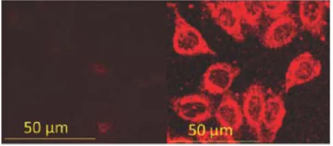
between a sulfonated aluminum phtalocyanine and gold nanorods or nanocubes to enhance their fluorescence.180They used it for
fluores-cence imaging of cancer cells using two-photon excitation in the NIR (Fig.10).
Since the chromophore to particle distance is a crucial parameter in the control of the charge or energy transfers between the two systems, several spacing strategies were investigated. The synthesis of block copolymers bearing chromophores along the chains showed efficient control over the distance by playing with the polymer structure.181,182
The copolymer functionalized with Lucifer Yellow (LY) allowed preparation of luminescent gold hybrid nanostructure (Fig. 11).181
The optimized nanostructures were successfully used for cell imaging and photodynamic therapy of cancer cells.181
Among the most investigated strategies is the use of core shell nanostructures with metal core and silica based shell, which provides also a good possibility of spacing control between the dyes and the metallic surface.183–192The dye can be either directly incorporated in
the silica shell during the synthesis of post-grafted at the surface of the silica. M. A. Noginov used this configuration to generate core-shell structure functionalized at the surface by Oregon green 488 fluorophore encapsulated in the outer silica shell.193 This structure,
with a spherical gold core of 14 nm in diameter and a silica shell of 15 nm thickness, allowed the demonstration of a spaser-based nanolaser in the visible range.193Murphy and co-workers showed that
it was possible to have a fine tuning of the distance and easy surface grafting using click-chemistry reactions (Fig.12a).186They observed
B3144 Journal of The Electrochemical Society,165(8) B3137-B3156 (2018)
Figure 9. Synthesis of polymer-modified NCs, redrawn according to a),85b)156and c).158
Hybrid materials for biomedical applications.— Nanomateri-als are novel systems with the potential applications for imag-ing and therapeutic.193–197 Nanoparticulate imaging and
therapeu-tic agents exhibit several advantages, including tunable size, high agent loading, tailorable surface properties, controllable or stimuli-responsive drug release kinetics, improved pharmacokinetics, and biocompatibility.198–200 Nanoparticles can be specifically targeted to
certain regions of the body (i.e. tumor regions) by conjugation with tar-geting ligands to enhance their accumulation in the intended parenchy-mal sites. They can also be engineered to contain multiple agents (i.e. imaging and therapeutic agents) for real-time monitoring of the drug uptake and/or therapeutic responses. Both of these features are difficult
Figure 10. Two-photon fluorescence imaging of cancer cell lines using pure
aluminum phtalocyanine (left) and aluminum phtalocyanine combined with gold nanocubes (right) (Reproduced with permission from Ref.180, copyright 2014, American Chemical Society).
to achieve with conventional small molecule drugs. A large number of nanoparticle platforms for biomedical applications have received clinical approval or are in clinical trials.193,196,201 The nanoparticle
platforms that have been extensively explored for biomedical applica-tions are predominantly either purely inorganic or organic materials. The archetypical inorganic nanoparticles, quantum dots (QDs), are nanomaterials generally composed of elements from either groups II and VI or III and V.202–206They display unique optical properties,
in-cluding sharp and symmetrical emission spectra, high quantum yields, broad absorption spectra, good chemical and photo-stability, and tun-able size-dependent emission wavelengths.204Another class of
inor-ganic nanoparticles that have been evaluated for biomedical imaging applications are metal oxides, such as superparamagnetic iron ox-ide nanoparticles (SPIO). Iron oxox-ide nanoparticles have been used as contrast agents for magnetic resonance imaging (MRI), and one for-mulation of SPIO has received FDA approval for clinical use.197Gold
nanoparticles with controllable morphologies have been extensively used for biological imaging applications as they can be engineered to exhibit strong absorption in the NIR region.207–210Hybrid
nanopar-ticles are composed of both inorganic and organic components that cannot only retain the beneficial features of both inorganic and organic nanomaterials, but also possess unique advantages over the other two types. For example, the ability to combine a multitude of organic and inorganic components in a modular fashion allows for systematic tuning of the properties of the resultant hybrid nanomaterial.
[image:8.585.38.280.603.709.2]Figure 11. Chemical structure of the diblock copolymer functionalized with LY dyes and AuNPs bearing the luminescent polymers. (Reproduced with permission from Ref.181, copyright 2013, Elsevier).
noncovalent interactions. This method was widely used to incorporate luminescent dyes (such as the cationic fluorophore Ru(bpy)3)2+within the anionic silica matrix.211However, the entrapped fluorophore can
leach out of the nanoparticle under physiological conditions, poten-tially complicating the data interpretation. Alternatively, imaging or therapeutic agents can be covalently incorporated into silica
nanopar-ticles by using trialkoxysilane-derived molecules that contain suitable imaging or therapeutic moieties. These molecules are incorporated within the silica matrix through silanol linkages during particle syn-thesis, leading to stable hybrid silica nanoparticles with uniform agents throughout the nanoparticle that are protected from the environment. The silica nanoparticles can also be post-synthetically modified by
Figure 12. a) Strategy using click chemistry on silica to bind the dyes and control the distance to the metal surface (top) (reproduced with permission from Ref.
[image:9.585.52.535.334.722.2]B3146 Journal of The Electrochemical Society,165(8) B3137-B3156 (2018)
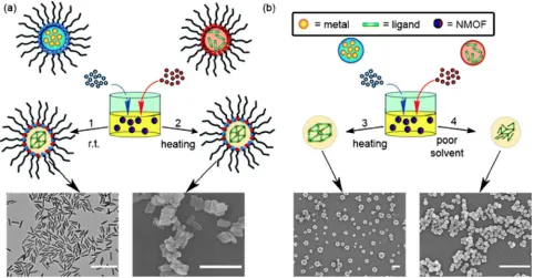
Figure 13. Schematic representation of various methods for making NMOF materials. (a) Water-in-oil, (b) Non-surfactant mediated methods: heating a solution
of the metal and the ligand in a coordinating solvent, and EM micrographs show NMOFs of Gd-ligand (reproduced with permission from Ref.219, copyright 2012, Elsevier).
reacting with trialkoxysilane molecules. Post-synthesis grafting is par-ticularly useful for modifying the particle surface with selected agents that are not stable during the silica particle synthesis. The synthetic versatility also allows the incorporation of imaging and therapeutic cargoes in multi-step sequences. After the desired organic function-ality is attached to the silica nanoparticles, the nanoparticles can be further modified through the additional functional group using tradi-tional conjugation chemistry. For example, an amine-modified par-ticle can be reacted with various carboxylate-containing molecules to form a stable amide bond. The cargoes can also be conjugated to the nanoparticle surface by electrostatic interactions. Several types of other inorganic nanoparticles have also been embedded into the silica nanoparticle core to impart imaging functionalities.212,213
Hybrid materials for imaging applications.—Nano metal-organic frameworks (MOFs), or coordination polymers are built from tran-sition metal ions and polydentate bridging ligands. Bulk MOFs have shown promise in a number of applications, including non-linear optics,214 selective catalysis,215 gas storage,216,217 and
chem-ical sensing.218 By scaling the materials down to the nano-regime,
these materials can be used for biomedical applications. In the silica-based nanomaterials described above, the silica matrix acts as a support for biomedically relevant moieties. In contrast, nano MOF (NMOF) particles can have these moieties incorporated within the framework structure as either the metal connecting points or the bridging ligands.219 NMOF nanoparticles are primarily
synthe-sized by four methods reverse microemulsion, surfactant-mediated hydrothermal synthesis, hydrothermal synthesis, and nanoprecipi-tation (Fig. 13). The first three methods generally lead to crys-talline nanomaterials whereas the fourth method tends to afford amorphous nanomaterials. NMOF particles have also been coated with biocompatible polymers via coordination to the surface metal centers.220,221Horcajada and coworkers successfully conjugated
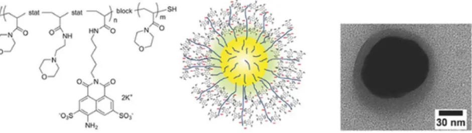
sev-eral biocompatible polymers (poly(ethylene glycol), dextran, and chitosan) to a variety of iron-carboxylate NMOF particles. Boyes and coworkers have coated Gd-NMOFs previously described by the Lin group222with a copolymer of poly(N-isopropylacrylamide)-co-poly(N-acryloxysuccinimide)-co-(fluoresceinO-methacrylate) by
RAFT polymerization.221 Additional imaging contrast agents
(sub-stances used to increase the visibility of structures or fluids within the body in medical imaging) or therapeutic moieties could be conjugated to the polymer through the succinimide group.
There have been numerous reports on incorporating organic flu-orophores into solid silica nanoparticles (SNPs) for optical imaging. In 2004, Tan and coworkers reported the synthesis of fluorescein isothiocyanate doped SNPs probes in reverse microemulsions.223The
resulting 70 nm NPs were conjugated with the TAT peptide, a cellu-lar penetratingpeptide, and used to label human lung cancer cells in vitro. The in vivo utility of these nanoparticles was demonstrated by selectively labeling rat brain blood vessels via intra-arterial delivery. After the procedure was completed, the brain was imaged using flu-orescence microscopy, and nanoparticle fluflu-orescence was observed in brain vessels. These results showed that the TAT-conjugated NPs could selectively cross the blood brain barrier and serve as a poten-tial way to deliver diagnostic or therapeutic agents to the brain. The efficacy of the hybrid SNPs as a dual optical and MR contrast agent was also demonstrated in a collagen-induced arthritis mouse model at 9.4 T.224Mice were injected with saline, 125 mg/kg, or 250 mg/kg of
hybrid SNPs in two doses separated by 6 hours. Luminescence inten-sity of the paws was measured with a clinical scanner the following day. All control mice displayed minimal luminescence compared to those which received the nanoparticle dose (Fig.14). The level of lu-minescence corresponded with the dose received, the clinical disease index, and the level of paw swelling.
Functionalized dye incorporated SNPs with a variety of active groups including hydroxyl, thiol, amine, and carboxyl.225The surface
Figure 14. Upper Control animals that did not have arthritis intravenously injected with two separate doses of (A) saline, (B) 125 mgMNP/kg, or (C) 250 mg MNP/kg 12 hours before optical imaging. (lower) CIA animals with arthritis intravenously injected with (D) saline, (E) 125 mg MNP/kg, or (F) 250 mg/kg, (reproduced with permission from Ref.223, copyright 2004, Royal Chemical Society).
surface of SNPs containing Nile Red with amine groups and conju-gated the targeting moieties apo-transferrin and folic acid. Both of these targeting moieties resulted in increased uptake of the particles by HeLa cells in vitro.
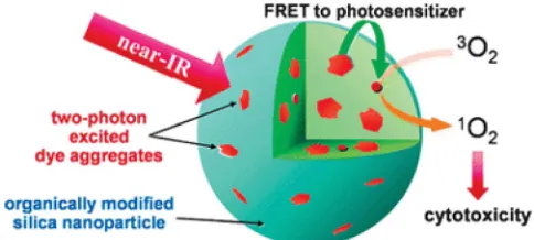
Hybrid SNPs have been used in drug delivery and therapy ap-plications. Prasad and coworkers described the use of an organically modified silica nanoparticle for photodynamic therapy (PDT).227PDT
is a light-activated treatment for cancer and other diseases, and works by utilizing light sensitive drugs (i.e. photosensitizers) that can be preferentially localized in malignant tissues. Its therapeutic effect is initiated by photoexcitation of the localized photosensitizer to gener-ate cytotoxic species such as singlet oxygen (1O
2). This leads to selec-tive and irreversible destruction of diseased tissues, without damaging adjacent healthy ones. The main drawback to this therapy is that cur-rently approved PDT photosensitizers absorb in the visible spectral region below 700 nm, where light penetration into the skin is only a few millimeters. This problem can be overcome by combining a two-photon absorbing (TPA) dye with the photosensitizer. Here, the photosensitizer is indirectly excited through fluorescence resonance energy transfer (FRET). In this work, a known photosensitizer and a two-photon energy donor were co-encapsulated in 30 nm silica NPs (Fig.15). Upon two-photon irradiation, the photosensitizer is excited
Figure 15. Representation of an organically modified SNP co-encapsulating
a photosensitizing drug and photon absorbing fluorescent dye aggregates for two-photon photodynamic therapy, (reproduced with permsssion from Ref. 227, copyright 2007, American Chemical Society).
as a result of intraparticle FRET from the two-photon absorbing dye, resulting in the generation of singlet oxygen. The uptake of these par-ticles was demonstrated through fluorescence imaging of HeLa cells. Upon two-photon irradiation, HeLa cells that had been incubated with the nanoparticles exhibited drastic morphology changes associated with cell necrosis, apparently induced by the reactive oxygen species generated by the photosensitizer.
Mesoporous SNPs (MSNPs) have been extensively evaluated as delivery vehicles for a variety of cargoes. Victor Lin and coworkers have also developed several MSNP-based delivery systems contain-ing stimuli-responsive pore caps (such as CdS, Au, and superparam-agnetic Fe3O4NPs) to allow for the controlled release of entrapped molecules.228,229As an example shown in Fig.16, the gold
nanopar-ticles were conjugated to the MSNP materials with a photolabile linker.230 The hybrid system releases the Au nanoparticle pore caps
when exposed to UV. This system was used to deliver paclitaxel to human liver and fibroblast cells. Other drug molecules and neuro-transmitters, such as vancomycin and adenosine triphosphate (ATP), have also been delivered using this strategy.228,229
A double drug delivery system was also developed based on capped MSNPs.231 Boronic acid functionalized MSNPs were loaded with
cyclic adenosine monophosphate (cAMP), an important cellular sig-naling molecule. The pores of the material were then capped with fluorescein-labeled insulin. Release from the material was shown to be triggered by saccharides, as they form more stable conjugates with the boronic acids on the nanoparticles. Feng and coworkers demon-strated the use of a cross-linked polymer network as a “gatekeeper” for MSNPs (Fig. 17).232 2-nm thick poly(N-acryloxysuccinimide)
was anchored to the MSNPs surface through reversible addition-fragmentation chain transfer (RAFT) polymerization and then cross-linked by adding cystamine. The ability to control the release of cargos was demonstrated by entrapping rhodamine B inside the MSN before cross-linking of the polymer. A light-activated nanoimpeller-controlled drug carrier based on MSNs was recently designed by taking advantage of the well-known cis-trans isomerizationin the azobenzene derivative (4-phenylazoaniline).233The anti-cancer drug
[image:11.585.38.280.590.699.2]B3148 Journal of The Electrochemical Society,165(8) B3137-B3156 (2018)
Figure 16. Graphical sketch of the AuNP -capped MSNP-based drug delivery
system, (reproduced with persmission from Ref.230, copyright 2009, Ameri-can Chemical Society).
was developed by Wang and coworkers for controlled delivery of doxorubicin in vitro.234
Hybrid materials for electronics.—Future ubiquitous electronic devices require versatile features, such as being lightweight and ex-hibiting portability, wearability and flexibility with a superior mechan-ical stability. Organic materials offer structural flexibility, convenient processing, tunable electronic properties, photoconductivity, efficient luminescence, and the potential for semiconducting and even metallic behavior. Inorganic compounds provide the potential for high car-rier mobilities, bandgap tunability, a range of magnetic and dielectric
properties, and thermal and mechanical stability. In addition to com-bining distinct characteristics, new or enhanced phenomena can also arise as a result of the interface between the organic and inorganic components. Electron-transfer processes at organic-inorganic inter-faces have, for example, been examined.235–237Dielectric modulation
in organic-inorganic systems has also led to enhanced binding ener-gies for excitons in the inorganic framework of the structure, as a result of the smaller dielectric constant and reduced screening in the organic component of the hybrid.238
In electronic materials polymer solar cells have attracted enough attention over the past several decades due to their advantageous prop-erties, including lightweight, flexibility, and solution processability.239
However, the electron mobility of most of conjugated polymers (CPs) is a few orders of magnitude lower than their hole mobility, thereby resulting in the charge carrier recombination in photoactive layer. In this regard, incorporating electron acceptors such as fullerene derivatives or semiconductor inorganic nanocrystals (NCs) is of key importance.240The bulk-heterojunction structure has been recognized
as the most successful architecture for polymer solar cells.241–244
Re-cently, BHJ solar cells composed of CPs and fullerene have achieved energy conversion efficiency up to 6∼8%.244 Inorganic
nanocrys-tals (NCs) possess size-dependent optical and electronic properties that open up opportunities for use in solar cells,245 LEDs,246
tun-able lasers,247 bio-sensors,248 and bio-imaging applications.249 In
particular, incorporating NCs (e.g., CdS, CdSe, CdTe, PbS, ZnO, etc.) in polymer solar cells would facilitate the charge dissociation and transport owing to the large surface area, high electron affin-ity, and excellent intrinsic carrier mobility of NCs.250 In this
con-text, semiconductor NCs have been introduced as electron accep-tors into hybrid solar cells (e.g., poly(3-hexylthiophene)/CdSe NCs; P3HT/CdSe).251,252 However, simply physically mixing CP and NC
often results in micro-scale phase segregation, thus limiting the re-sulting device performance.253–254In addition, the insulating organic
ligands capped on the NC surface hinder the electronic interaction with CPs. As a result, the ability to directly tether CPs on the NC surface would be an elegant means of achieving the intimate contact between CPs and NCs to prevent such microscopic aggregation. To this end, direct grafting and in-situ growth methods have been ex-plored to create CP-grafted NCs and naked NCs in the CP matrix, respectively, for hybrid solar cells.255However, polymer based solar
cells often suffer from insufficient light absorption despite the strong absorption coefficient of most CPs. This is because the thickness of photoactive layer is restricted due to the short charge carrier diffusion length as well as the use of large bandgap of CPs which fails to absorb solar photons in NIR region. In this regard, plasmonic metallic NCs (e.g., Au and Ag) and NIR-absorbing NCs (e.g., PbS and PbSe) have been utilized to further harvest solar energy.256Moreover, despite the
Figure 17. Representation of redox responsive nano-gated
[image:12.585.36.356.551.754.2]Figure 18. Graphic representation of operating principles of an organic-inorganic solar cell. The electron (●) and hole (◦) transfer are shown with arrows, (reproduced with permission from Ref.257, copyright 2013, Royal Society of Chemistry).
significant developments in interfacial treatment for efficient charge separation, control over the architecture of photoactive layer com-prising CP/NC nanocomposites has not yet been exploited to its full potential for charge transport due largely to the difficulty in control-ling the film morphology during the spin-casting process. Ideal device geometry should consist of bicontinuous pathway for both holes and electrons, and thus enhance charge transport as well as reduce the charge recombination.
So called 1st generation solar cells based on crystalline and poly-crystalline silicon (Si) with power conversion efficiencies (PCE) in the range 18–25% are still dominating the photovoltaics (PV) market. 2nd generation thin film solar cells based on II-VI semiconductors, copper indium gallium selenide, and amorphous Si possessed the best PCE of close to 20%.257The 3rd generation solar cells were
devel-oped to pursue high PCE and low costs for special applications, such as tandem cells, light-condensed cells, organic photovoltaics, dye-sensitized solar cells, organic-inorganic hybrid solar cells and so on. Generally, the PCEs and lifetimes of solar cells containing organic components were less efficient than those of traditional 1st and 2nd generation solar cells. However, the low fabrication cost, flexibility and light weight have made them suitable for several special appli-cations. Organic-inorganic hybrid solar cells could adopt the merits of inorganic materials, such as stability, high carrier mobility and compatible fabricating process, and utilize the advantages of organ-ics, such as enhanced light absorption at a wide range of wavelengths, adjustable molecular structures for energy band alignment, facile solu-tion processability, and so on. Similar to the Si p-n juncsolu-tion solar cells, the general operating principle of organic-inorganic hybrid solar cells also involves the following steps: light absorption, exciton generation and diffusion, exciton dissociation to carriers at the junction inter-face and carrier transportation and collection, which is schematically shown in Fig.18.
Lot of effort has been made to improve the performance of hy-brid solar cells. Based on the interface configuration of p-n junctions, hybrid solar cells have been developed by three methods, which are schematically shown in Fig.19.257The deposition of an organic film
on an inorganic film can instantly form an hybrid solar cell, as depicted in Fig.19a. Sandwiched blend of inorganic QDs, NPs and nanowires (NWs) with organic semiconductors shown in Fig. 19b. The main advantage of this configuration is the cost-effectiveness and flexibility of the fabrication process. However, dead-ends (domains which does not produce photocurrent) and short circuiting of charges could not be avoided in this type of solar cell. In order to further enlarge the in-terface area and benefit carrier transportation, ordered nanostructures were adopted for use in hybrid solar cells, as in Fig.19c.
Many reviews have highlighted the development and prospects of hybrid solar cells. Due to their facile and cost-effective fabrication,
shown in Fig.17b.258–260The maximum PCE achieved was about 5%
and a theoretical prediction of 10% has been reported.261,262 Their
performance was dominated by the absorption spectra of the active components, the interface morphology of the junction, and the blend-ing composition.263–266 The synthesis route, dispersed solvents and
surface termination of inorganic QDs/NPs also affected the properties of the Hybrid solar cells.267Polystyrene sphere template-assisted
syn-thesis can generate several kinds of one-dimensional nanostructured arrays, such as nanopillars, nanorods, and NWs.268The state-of-the-art
research on hybrid organic-inorganic solar cells based on nanostruc-tured arrays have been explored.269–270The most popular organics for
hybrid solar cells are summarized in Fig.20. The balance between performance in practical applications and cost may be one of the important considerations for developments in the near future.
Hybrid materials for electrical memory devices.—Functional hy-brid inorganic/organic nanocomposites provide a frontier for unique functions with promising applications in nonvolatile memory de-vices. Organic bistable devices fabricated utilizing nanocomposites have emerged as excellent candidates for potential applications in the next-generation nonvolatile memory devices. A typical structure for a hybrid organic/inorganic nonvolatile memory device consists of composite organic molecules: metal/semiconductor nanoparticles layer sandwiched between two metal electrodes. The device area is defined by the overlap between the top and the bottom electrodes; therefore, a very high memory density can be easily achieved by us-ing cross-bar arrays.271–275The organic material used can consist of
small organic molecules or polymers. Small organic molecules have low molecular weight and can be deposited under high vacuum with-out decomposition by using thermal evaporation. Polymer molecules, on the other hand, consist of much larger molecules with long chains of repeating monomer units and will decompose before evaporation begins. One of the main advantages provided by organic materials and devices is low fabrication cost and simplicity. The fabrication of these devices through thermal evaporation requires high vacuum and stringent conditions to control the morphology of the organic active layer.276As alternatives to the more elaborate processes of
vac-uum evaporation and deposition of organic and inorganic molecular materials, solution processes, including spin-coating, spray-coating, dip-coating, roller-coating and ink-jet printing, are well known and can be used to deposit polymer materials on a variety of substrates, such as glasses, plastics, metal foils and wafers.277–280 The simplest
structure for a hybrid memory device fabricated utilizing the solution method is a single-polymer layer embedded with inorganic nanoma-terials and sandwiched between two metal electrodes, as shown in Fig.21.277Fabrications of single-layer-structured nonvolatile
memo-ries based on various organic/inorganic hybrid nanocomposites have been reported. Inorganic species used in these memories include semi-conductor nanoparticles (ZnO, CdSe, Si, CuO and so on) and metal nanoparticles (Au, Ag, FeNi and so on).277–287
[image:13.585.306.547.66.137.2]B3150 Journal of The Electrochemical Society,165(8) B3137-B3156 (2018)
Figure 20. Chemical structure and abbreviations of the organic semiconductor components in hybrid solar cells.
resistor or one transistor and one resistor structures to construct an individual memory cell with high reading accessibility.278,279
There-fore, multilayer structures might be required to realize one diode/one resistor or one transistor/one resistor cells. Some works concerning the formation of multilayer-structured nonvolatile memory devices by using PI materials have been reported, and their memory effects have been demonstrated as well.280–282Depending on theI-V
characteris-tics, three types of nonvolatile memory effects, write-once-read-many-times and unipolar and bipolar electrical switching, can be observed for hybrid devices. In the case of a nonvolatile memory based on hy-brid nanocomposites, the memory effect is strongly correlated with the presence of inorganic nanomaterials, for example, ZnO QDs, Au nanoparticles, CdSe nanoparticles and carbon nanotubes, embedded in a polymer matrix because the current difference between the ON and the OFF states for the polymer-only device is negligible.283Recently,
for a hybrid device containing Au QDs embedded in a PI layer, Wu et al.284 reported an electrical bistability with an ON/OFF ratio of
∼108, which is one of the largest values for a stable hybrid mem-ory device. In the case of a unipolar nonvolatile memmem-ory, due to the presence of a negative differential resistance in theI-V characteris-tics, the OFF state can be regained when a forward bias is given
Figure 21. Schematic representation of the hybrid memory device,
(repro-duced with permission from Ref.277a, copyright 2012, Nature Publishing Group).
to the memory device.285,286For bipolar memories, the OFF state of
the hybrid device can be recovered by applying a reverse bias volt-age, which is equivalent to the ‘erasing’ process in a digital memory cell. One of the main advantages of a nonvolatile memory device based on hybrid nanocomposites is the possibility of realizing flexi-ble memories at extremely low fabrication cost. These hybrid devices can be processed at low temperatures and, therefore, are regarded as one of the most important types of information-storage components for future stretchable/portable electronic device applications.287–291
For example, Kim and Lee287developed nonvolatile memory devices
on plastic substrates (PES) based on a pentacene layer embedded with self-assembled gold nanoparticles, as shown in Fig. 22. The nano floating gate memory exhibited a large memory window that could be maintained for>1 year. Nonvolatile electrical bistability of a hybrid device fabricated utilizing CdSe/ZnS nanoparticles embed-ded in a conducting poly(N-vinylcarbazole) polymer layer on flexi-ble polyvinylidene difluoride and polyethylene terephthlate substrates has also been reported.291The results indicate that the hybrid bistable
memory devices are prospects for potential applications in flexible nonvolatile flash memory devices.291
Also, the area of functional organic thin film transistors (OTFTs) have attracted extensive research efforts in recent years because of their tremendous emerging impact on applications for flexible electronics.292–296 Especially, OTFTs can serve as the basic and
re-liable media for electrical memories and switching devices in the increasingly important information technology. OTFTs with non-volatile memory effects are one potential option based on their nondestructive readout and single transistor architectural compat-ibility for easily integrated devices.297–301 Organic thin film
tran-sistor (OTFT)-based nonvolatile memory devices using the hy-brid nanocomposites of semiconducting
poly(9,9-dioctylfluorene-alt-bithiophene) (F8T2) and ligand-capped Au nanoparticles (NPs), thereby serving as a charge storage medium have been fabricated (Fig.23).302
[image:14.585.61.254.601.719.2]Figure 22. a) 3D representation diagram of the flexible hybrid memory device architecture. Patterned Ti/Au on a PES plastic substrate was used as the gate electrode, and a pentacene active layer and gold source/drain contacts were formed to make the organic transistor-based memory devices, b) Photograph of a fabricated flexible organic memory device, (reproduced with permission from Ref.287, copyright 2010, American Chemical Society).
Figure 23. Schematic representation of hybrid nonvolatile organic thin film transistor memory device based on semiconducting polymers and AuNPs, (reproduced
[image:15.585.113.472.569.714.2]B3152 Journal of The Electrochemical Society,165(8) B3137-B3156 (2018)
Figure 24. Schematics of a FeS2–PbS/GFET heterojunction and the corresponding charge transfer process before (a) and after (b) the ligand exchange.
Photore-sponse curves of FeS2–PbS/GFET heterojunction photodetectors on NIR illumination (1100 nm, 12μW/cm2,VDS=0.1 V) on/off, before ligand exchange (c)
and after (d), (reproduced with permission from Ref.311, copyright 2017, American Chemical Society).
integrated in modern electronics and related multidisciplinary fields at an exponentially increasing rate. Stretchable electronics, which builds electronic circuits on top of a stretchable substrate or em-beds them in a stretchable matrix, enables devices to be deformed into arbitrary shapes while maintaining the performance and reli-ability of the devices.303,304 Flexible electronics have gained
con-siderable research interest in the recent years because of their spe-cial features and potential applications in flexible displays, artifi-cial skins, sensors, sustainable energy, etc. With unique geometry, outstanding electronic/optoelectronic properties, excellent mechani-cal flexibility and good transparency. Flexible electronics fabricated on large area polymeric substrates is an emerging field with a wide range of applications in areas such as displays, health monitor-ing devices, smart clothmonitor-ing, radio frequency identification devices (RFIDs), and energy storage.305–309 Novel printable
nanocompos-ite photosensitizer consisting of colloidal nanocrystals of FeS2 and
PbS with complementary optical and microstructural properties for broadband photodetection. Using a newly developed ligand exchange to achieve high-efficiency charge transfer across the nanocomposite FeS2-PbS sensitizer and graphene on the FeS2-PbS/graphene photo-conductors, an extraordinary photoresponsivity in exceeding arpound 106 A/W was obtained in an ultrabroad spectrum of ultraviolet-visible-near-infrared (Fig. 24).310 Printable highly conductive
cath-ode interfacial layer (CIL) for efficient polymer solar cells by sen-sitizing ZnO nanocrystals with a blue fluorescent conjugated poly-mer, poly(9,9-bis-(6-diethoxylphosphorylhexyl) fluorene) was also fabricated.311 More recently, to realize green and flexible
electron-ics, ultrastrong, transparent, conductive and printable nanocompos-ites were successfully prepared by mixing single-walled carbon nan-otubes with 2,2,6,6-tetramethylpiperidine-1-oxyl-oxidized cellulose nanofibrils with abundant sodium carboxyl groups on the crystalline nanocellulose surfaces.312
Figure 25. Inkjet printed poly(NVK-co-MAH)-g-P1@Ag nanosphere ink: (a) SEM image of the printed square grids on (1×1 cm2) on glass substrate. Inkjet
[image:16.585.113.475.620.726.2]